 | –≠–ª–µ–∫—Ç—Ä–æ–Ω–Ω—ã–π –∫–æ–º–ø–æ–Ω–µ–Ω—Ç: BC549 | –°–∫–∞—á–∞—Ç—å:  PDF PDF  ZIP ZIP |
DATA SHEET
Product specification
Supersedes data of 1997 Jun 20
1999 Apr 22
DISCRETE SEMICONDUCTORS
BC549; BC550
NPN general purpose transistors
book, halfpage
M3D186
1999 Apr 22
2
Philips Semiconductors
Product specification
NPN general purpose transistors
BC549; BC550
FEATURES
∑
Low current (max. 100 mA)
∑
Low voltage (max. 45 V).
APPLICATIONS
∑
Low noise stages in audio frequency equipment.
DESCRIPTION
NPN transistor in a TO-92; SOT54 plastic package.
PNP complements: BC559 and BC560.
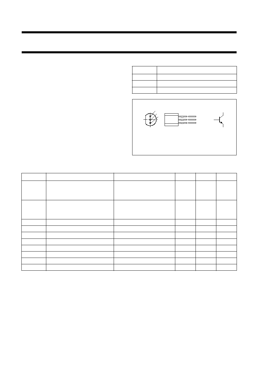
PINNING
PIN
DESCRIPTION
1
emitter
2
base
3
collector
Fig.1
Simplified outline (TO-92; SOT54)
and symbol.
handbook, halfpage
1
3
2
MAM182
3
2
1
LIMITING VALUES
In accordance with the Absolute Maximum Rating System (IEC 134).
Note
1. Transistor mounted on an FR4 printed-circuit board.
SYMBOL
PARAMETER
CONDITIONS
MIN.
MAX.
UNIT
V
CBO
collector-base voltage
open emitter
BC549
-
30
V
BC550
-
50
V
V
CEO
collector-emitter voltage
open base
BC549
-
30
V
BC550
-
45
V
V
EBO
emitter-base voltage
open collector
-
5
V
I
C
collector current (DC)
-
100
mA
I
CM
peak collector current
-
200
mA
I
BM
peak base current
-
200
mA
P
tot
total power dissipation
T
amb
25
∞
C; note 1
-
500
mW
T
stg
storage temperature
-
65
+150
∞
C
T
j
junction temperature
-
150
∞
C
T
amb
operating ambient temperature
-
65
+150
∞
C

1999 Apr 22
3
Philips Semiconductors
Product specification
NPN general purpose transistors
BC549; BC550
THERMAL CHARACTERISTICS
Note
1. Transistor mounted on an FR4 printed-circuit board.
CHARACTERISTICS
T
j
= 25
∞
C unless otherwise specified.
Notes
1. V
BEsat
decreases by about 1.7 mV/K with increasing temperature.
2. V
BE
decreases by about 2 mV/K with increasing temperature.
SYMBOL
PARAMETER
CONDITIONS
VALUE
UNIT
R
th j-a
thermal resistance from junction to ambient
note 1
250
K/W
SYMBOL
PARAMETER
CONDITIONS
MIN.
TYP.
MAX.
UNIT
I
CBO
collector cut-off current
I
E
= 0; V
CB
= 30 V
-
-
15
nA
I
E
= 0; V
CB
= 30 V; T
j
= 150
∞
C
-
-
5
µ
A
I
EBO
emitter cut-off current
I
C
= 0; V
EB
= 5 V
-
-
100
nA
h
FE
DC current gain
BC549C; BC550C
I
C
= 10
µ
A; V
CE
= 5 V; see Fig.2
-
270
-
I
C
= 2 mA; V
CE
= 5 V; see Fig.2
420
520
800
V
CEsat
collector-emitter saturation voltage
I
C
= 10 mA; I
B
= 0.5 mA
-
90
250
mV
I
C
= 100 mA; I
B
= 5 mA
-
200
600
mV
V
BEsat
base-emitter saturation voltage
I
C
= 10 mA; I
B
= 0.5 mA; note 1
-
700
-
mV
I
C
= 100 mA; I
B
= 5 mA; note 1
-
900
-
mV
V
BE
base-emitter voltage
I
C
= 2 mA; V
CE
= 5 V; note 2
580
660
700
mV
I
C
= 10 mA; V
CE
= 5 V; note 2
-
-
770
mV
C
c
collector capacitance
I
E
= i
e
= 0; V
CB
= 10 V; f = 1 MHz
-
1.5
-
pF
C
e
emitter capacitance
I
C
= i
c
= 0; V
EB
= 0.5 V; f = 1 MHz
-
11
-
pF
f
T
transition frequency
I
C
= 10 mA; V
CE
= 5 V;
f = 100 MHz
100
-
-
MHz
F
noise figure
I
C
= 200
µ
A; V
CE
= 5 V;
R
S
= 2 k
; f = 10 Hz to 15.7 kHz
-
-
4
dB
I
C
= 200
µ
A; V
CE
= 5 V;
R
S
= 2 k
; f = 1 kHz; B = 200 Hz
-
-
4
dB

1999 Apr 22
4
Philips Semiconductors
Product specification
NPN general purpose transistors
BC549; BC550
Fig.2 DC current gain; typical values.
handbook, full pagewidth
0
600
200
400
MBH725
10
-
2
10
-
1
hFE
1
IC (mA)
10
10
3
10
2
VCE = 5 V
BC549C; BC550C.

1999 Apr 22
5
Philips Semiconductors
Product specification
NPN general purpose transistors
BC549; BC550
PACKAGE OUTLINE
UNIT
A
REFERENCES
OUTLINE
VERSION
EUROPEAN
PROJECTION
ISSUE DATE
IEC
JEDEC
EIAJ
mm
5.2
5.0
b
0.48
0.40
c
0.45
0.40
D
4.8
4.4
d
1.7
1.4
E
4.2
3.6
L
14.5
12.7
e
2.54
e1
1.27
L1
(1)
2.5
b1
0.66
0.56
DIMENSIONS (mm are the original dimensions)
Note
1. Terminal dimensions within this zone are uncontrolled to allow for flow of plastic and terminal irregularities.
SOT54
TO-92
SC-43
97-02-28
A
L
0
2.5
5 mm
scale
b
c
D
b
1
L1
d
E
Plastic single-ended leaded (through hole) package; 3 leads
SOT54
e1
e
1
2
3