 | –≠–ª–µ–∫—Ç—Ä–æ–Ω–Ω—ã–π –∫–æ–º–ø–æ–Ω–µ–Ω—Ç: BC847BVN | –°–∫–∞—á–∞—Ç—å:  PDF PDF  ZIP ZIP |
Document Outline
- FEATURES
- PINNING
- APPLICATIONS
- DESCRIPTION
- MARKING
- LIMITING VALUES
- THERMAL CHARACTERISTICS
- CHARACTERISTICS
- PACKAGE OUTLINE
- DATA SHEET STATUS
- DEFINITIONS
- DISCLAIMERS

DATA SHEET
Product specification
Supersedes data of 2001 Aug 30
2001 Nov 07
DISCRETE SEMICONDUCTORS
BC847BVN
NPN/PNP general purpose
transistor
M3D744
2001 Nov 07
2
Philips Semiconductors
Product specification
NPN/PNP general purpose transistor
BC847BVN
FEATURES
∑
300 mW total power dissipation
∑
Very small 1.6 mm x 1.2 mm ultra thin package
∑
Excellent coplanarity due to straight leads
∑
Replaces two SC-75/SC-89 packaged transistors on
same PCB area
∑
Reduced required PCB area
∑
Reduced pick and place costs.
APPLICATIONS
∑
General purpose switching and amplification
∑
Switch mode power supply complementary MOSFET
driver
∑
Complementary driver for audio amplifiers.
DESCRIPTION
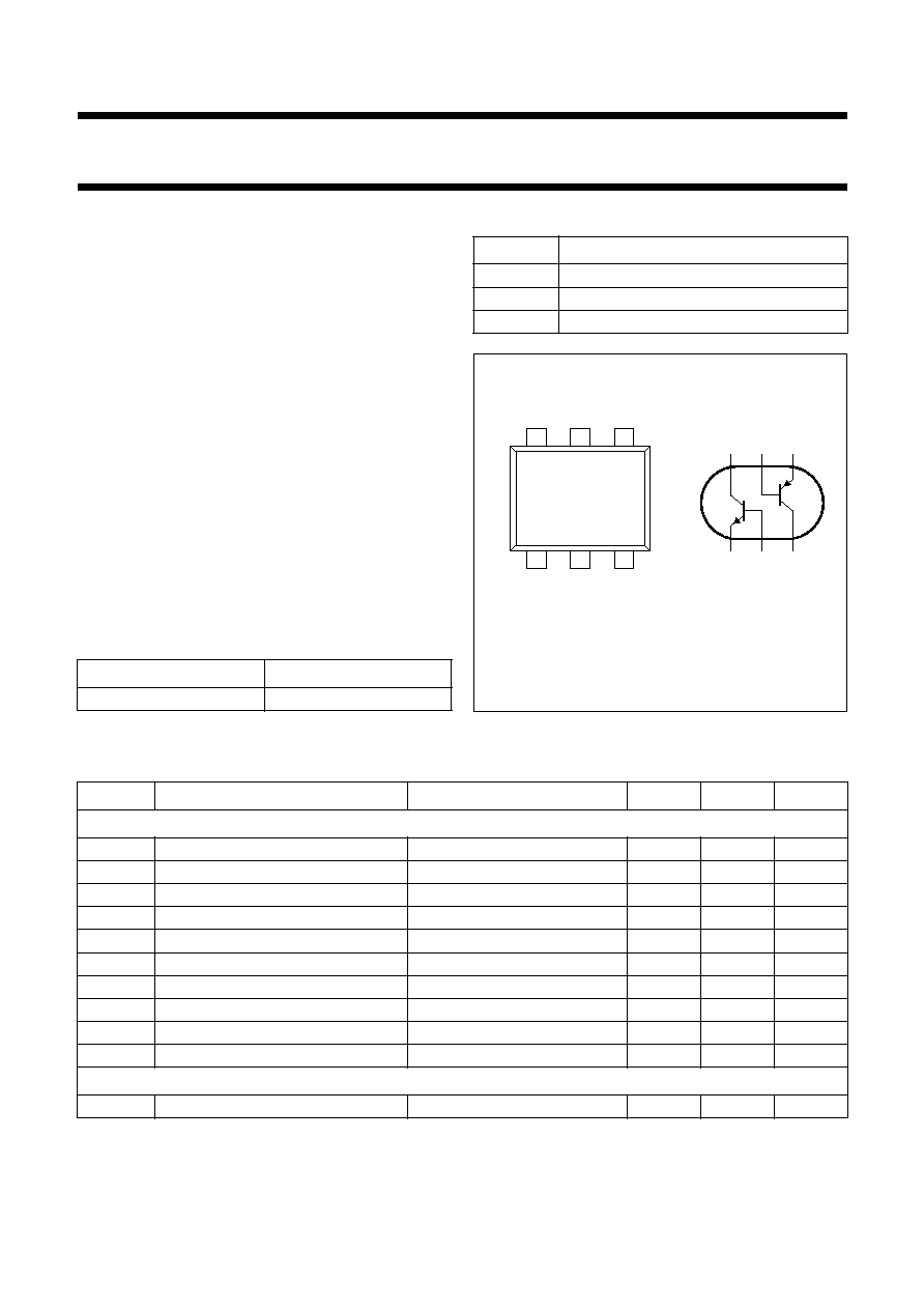
NPN/PNP transistor pair in a SOT666 plastic package.
MARKING
PINNING
TYPE NUMBER
MARKING CODE
BC847BVN
13
PIN
DESCRIPTION
1, 4
emitter
TR1; TR2
2, 5
base
TR1; TR2
6, 3
collector
TR1; TR2
handbook, halfpage
MAM443
1
3
2
TR1
TR2
6
4
5
1
2
3
4
6
5
Top view
Fig.1
Simplified outline (SOT666) and symbol.
LIMITING VALUES
In accordance with the Absolute Maximum Rating System (IEC 60134).
Note
1. Transistor mounted on an FR4 printed-circuit board.
SYMBOL
PARAMETER
CONDITIONS
MIN.
MAX.
UNIT
Per transistor; for the PNP transistor with negative polarity
V
CBO
collector-base voltage
open emitter
-
50
V
V
CEO
collector-emitter voltage
open base
-
45
V
V
EBO
emitter-base voltage
open collector
-
5
V
I
C
collector current (DC)
-
100
mA
I
CM
peak collector current
-
200
mA
I
BM
peak base current
-
200
mA
P
tot
total power dissipation
T
amb
25
∞
C; note 1
-
200
mW
T
stg
storage temperature
-
65
+150
∞
C
T
j
junction temperature
-
150
∞
C
T
amb
operating ambient temperature
-
65
+150
∞
C
Per device
P
tot
total power dissipation
T
amb
25
∞
C; note 1
-
300
mW

2001 Nov 07
3
Philips Semiconductors
Product specification
NPN/PNP general purpose transistor
BC847BVN
THERMAL CHARACTERISTICS
Notes
1. Transistor mounted on an FR4 printed-circuit board.
2. The only recommended soldering is reflow soldering.
CHARACTERISTICS
T
amb
= 25
∞
C unless otherwise specified.
Note
1. Pulse test: t
p
300
µ
s;
0.02.
SYMBOL
PARAMETER
CONDITIONS
VALUE
UNIT
R
th j-a
thermal resistance from junction to ambient
notes 1 and 2
416
K/W
SYMBOL
PARAMETER
CONDITIONS
MIN.
TYP.
MAX.
UNIT
Per transistor; for the PNP transistor with negative polarity
I
CBO
collector-base cut-off current
V
CB
= 30 V; I
E
= 0
-
-
15
nA
V
CB
= 30 V; I
E
= 0; T
j
= 150
∞
C
-
-
5
µ
A
I
EBO
emitter-base cut-off current
V
EB
= 5 V; I
C
= 0
-
-
100
nA
h
FE
DC current gain
V
CE
= 5 V; I
C
= 2 mA
200
-
450
V
CEsat
collector-emitter saturation
voltage
I
C
= 10 mA; I
B
= 0.5 mA
-
-
100
mV
I
C
= 100 mA; I
B
= 5 mA; note 1
-
-
300
mV
V
BEsat
collector-emitter saturation
voltage
I
C
= 10 mA; I
B
= 0.5 mA
-
755
-
mV
f
T
transition frequency
I
C
= 10 mA; V
CE
= 5 V; f = 100 MHz
100
-
-
MHz
NPN transistor
V
BE
base-emitter turn-on voltage
V
CE
= 5 V; I
C
= 2 mA
580
655
700
mV
C
c
collector capacitance
V
CB
= 10 V; I
E
= I
e
= 0; f = 1MHz
-
-
1.5
pF
C
e
emitter capacitance
V
EB
= 500 mV; I
C
= I
c
= 0; f = 1MHz
-
11
-
pF
PNP transistor
V
BE
base-emitter turn-on voltage
V
CE
=
-
5 V; I
C
=
-
2 mA
600
655
750
mV
C
c
collector capacitance
V
CB
=
-
10 V; I
C
= I
c
= 0; f = 1MHz
-
-
2.2
pF
C
e
emitter capacitance
V
EB
=
-
500 mV; I
E
= I
e
= 0; f = 1MHz
-
10
-
pF
2001 Nov 07
4
Philips Semiconductors
Product specification
NPN/PNP general purpose transistor
BC847BVN
handbook, halfpage
0
400
600
200
MLD703
10
-
1
1
10
IC (mA)
hFE
10
2
10
3
(1)
(3)
(2)
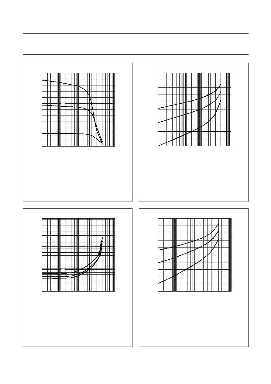
Fig.2
DC current gain as a function of collector
current: typical values.
TR1 (NPN); V
CE
= 5 V.
(1) T
amb
= 150
∞
C.
(2) T
amb
= 25
∞
C.
(3) T
amb
=
-
55
∞
C.
handbook, halfpage
200
1200
400
600
800
1000
MLD704
10
-
2
10
-
1
1
IC (mA)
VBE
mV
10
10
2
10
3
(3)
(2)
(1)
Fig.3
Base-emitter voltage as a function of
collector current; typical values.
TR1 (NPN); V
CE
= 5 V.
(1) T
amb
=
-
55
∞
C.
(2) T
amb
= 25
∞
C.
(3) T
amb
= 150
∞
C.
handbook, halfpage
10
4
10
3
10
2
10
MLD705
10
-
1
1
10
IC (mA)
VCEsat
(mV)
10
2
10
3
(2)
(1)
(3)
Fig.4
Collector-emitter saturation voltage as a
function of collector current: typical values.
TR1 (NPN); I
C
/I
B
= 20.
(1) T
amb
= 150
∞
C.
(2) T
amb
= 25
∞
C.
(3) T
amb
=
-
55
∞
C.
handbook, halfpage
200
1200
400
600
800
1000
MLD706
1
10
-
1
IC (mA)
VBEsat
(mV)
10
10
2
10
3
(1)
(3)
(2)
Fig.5
Base-emitter saturation voltage as a
function of collector current.
TR1 (NPN); I
C
/I
B
= 20.
(1) T
amb
=
-
55
∞
C.
(2) T
amb
= 25
∞
C.
(3) T
amb
= 150
∞
C.

2001 Nov 07
5
Philips Semiconductors
Product specification
NPN/PNP general purpose transistor
BC847BVN
handbook, halfpage
0
1000
200
400
600
800
MLD699
-
10
-
2
-
10
-
1
(1)
-
1
IC (mA)
hFE
-
10
-
10
2
-
10
3
(2)
(3)
Fig.6
DC current gain as a function of collector
current: typical values.
TR2 (PNP); V
CE
=
-
5 V.
(1) T
amb
= 150
∞
C.
(2) T
amb
= 25
∞
C.
(3) T
amb
=
-
55
∞
C.
handbook, halfpage
-
200
-
1200
-
400
-
600
-
800
-
1000
MLD700
-
10
-
2
-
10
-
1
(1)
-
1
IC (mA)
VBE
mV
-
10
-
10
2
-
10
3
(3)
(2)
Fig.7
Base-emitter voltage as a function of
collector current; typical values.
TR2 (PNP); V
CE
=
-
5 V.
(1) T
amb
=
-
55
∞
C.
(2) T
amb
= 25
∞
C.
(3) T
amb
= 150
∞
C.
handbook, halfpage
-
10
4
-
10
3
-
10
2
-
10
MLD701
-
10
-
1
-
1
-
10
IC (mA)
VCEsat
(mV)
-
10
2
-
10
3
(1)
(2)
(3)
Fig.8
Collector-emitter saturation voltage as a
function of collector current: typical values.
TR2 (PNP); I
C
/I
B
= 20.
(1) T
amb
= 150
∞
C.
(2) T
amb
= 25
∞
C.
(3) T
amb
=
-
55
∞
C.
handbook, halfpage
-
200
-
1200
-
400
-
600
-
800
-
1000
MLD702
-
1
-
10
-
1
IC (mA)
VBEsat
(mV)
-
10
-
10
2
-
10
3
(1)
(3)
(2)
Fig.9
Base-emitter saturation voltage as a
function of collector current.
TR2 (PNP); I
C
/I
B
= 20.
(1) T
amb
=
-
55
∞
C.
(2) T
amb
= 25
∞
C.
(3) T
amb
= 150
∞
C.