 | –≠–ª–µ–∫—Ç—Ä–æ–Ω–Ω—ã–π –∫–æ–º–ø–æ–Ω–µ–Ω—Ç: BC875 | –°–∫–∞—á–∞—Ç—å:  PDF PDF  ZIP ZIP |
DATA SHEET
Product specification
Supersedes data of 1997 Apr 22
1999 May 28
DISCRETE SEMICONDUCTORS
BC875; BC879
NPN Darlington transistors
book, halfpage
M3D186
1999 May 28
2
Philips Semiconductors
Product specification
NPN Darlington transistors
BC875; BC879
FEATURES
∑
High DC current gain (min. 1000)
∑
High current (max. 1 A)
∑
Low voltage (max. 80 V)
∑
Integrated diode and resistor.
APPLICATIONS
∑
Relay drivers.
DESCRIPTION
NPN Darlington transistor in a TO-92 (SOT54) plastic
package. PNP complement: BC878.
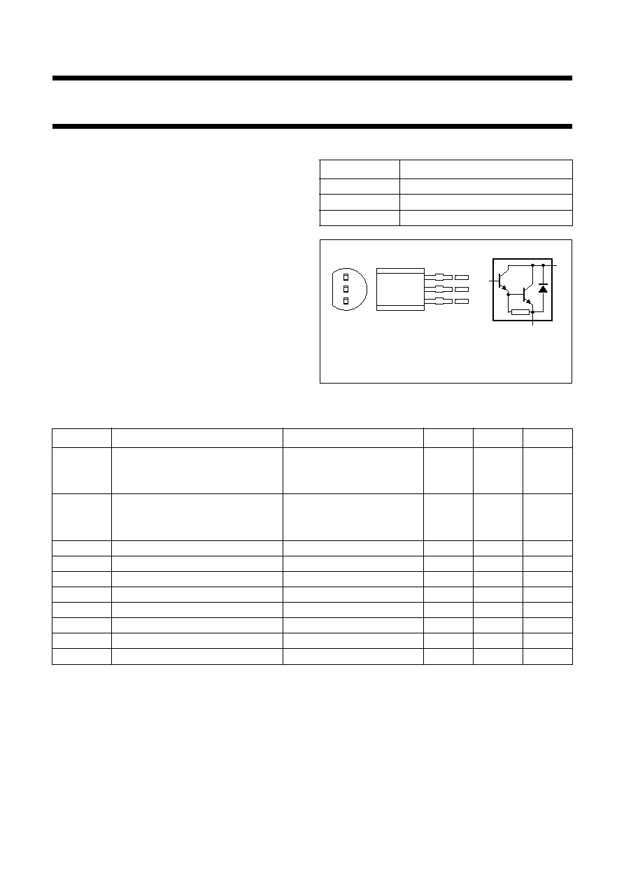
PINNING
PIN
DESCRIPTION
1
base
2
collector
3
emitter
Fig.1
Simplified outline (TO-92; SOT54)
and symbol.
handbook, halfpage
MAM307
1
2
3
1
2
3
LIMITING VALUES
In accordance with the Absolute Maximum Rating System (IEC 134).
Note
1. Transistor mounted on an FR4 printed-circuit board.
SYMBOL
PARAMETER
CONDITIONS
MIN.
MAX.
UNIT
V
CBO
collector-base voltage
open emitter
BC875
-
60
V
BC879
-
100
V
V
CES
collector-emitter voltage
V
BE
= 0
BC875
-
45
V
BC879
-
80
V
V
EBO
emitter-base voltage
open collector
-
5
V
I
C
collector current (DC)
-
1
A
I
CM
peak collector current
-
2
A
I
B
base current (DC)
-
0.2
A
P
tot
total power dissipation
T
amb
25
∞
C; note 1
-
0.83
W
T
stg
storage temperature
-
65
+150
∞
C
T
j
junction temperature
-
150
∞
C
T
amb
operating ambient temperature
-
65
+150
∞
C
1999 May 28
3
Philips Semiconductors
Product specification
NPN Darlington transistors
BC875; BC879
THERMAL CHARACTERISTICS
Note
1. Transistor mounted on an FR4 printed-circuit board.
CHARACTERISTICS
T
j
= 25
∞
C unless otherwise specified.
SYMBOL
PARAMETER
CONDITIONS
VALUE
UNIT
R
th j-a
thermal resistance from junction to ambient
note 1
150
K/W
SYMBOL
PARAMETER
CONDITIONS
MIN.
TYP.
MAX.
UNIT
I
CES
collector cut-off current
BC875
V
BE
= 0; V
CE
= 45 V
-
-
50
nA
BC879
V
BE
= 0; V
CE
= 80 V
-
-
50
nA
I
EBO
emitter cut-off current
I
C
= 0; V
EB
= 4 V
-
-
50
nA
h
FE
DC current gain
I
C
= 150 mA; V
CE
= 10 V; see Fig.2
1000
-
-
I
C
= 0.5 A; V
CE
= 10 V; see Fig.2
2000
-
-
V
CEsat
collector-emitter saturation voltage
I
C
= 0.5 A; I
B
= 0.5 mA
-
-
1.3
V
I
C
= 1 A; I
B
= 1 mA
-
-
1.8
V
V
BEsat
base-emitter saturation voltage
I
C
= 1 A; I
B
= 1 mA
-
-
2.2
V
f
T
transition frequency
I
C
= 0.5 A; V
CE
= 5 V; f = 100 MHz
-
200
-
MHz
Switching times (between 10% and 90% levels)
t
on
turn-on time
I
Con
= 500 mA; I
Bon
= 0.5 mA;
I
Boff
=
-
0.5 mA
-
500
-
ns
t
off
turn-off time
-
1300
-
ns

1999 May 28
4
Philips Semiconductors
Product specification
NPN Darlington transistors
BC875; BC879
Fig.2 DC current gain; typical values.
V
CE
= 10 V.
handbook, full pagewidth
0
5000
1000
2000
3000
4000
MGD838
10
-
1
1
IC (mA)
hFE
10
10
2
10
3

1999 May 28
5
Philips Semiconductors
Product specification
NPN Darlington transistors
BC875; BC879
PACKAGE OUTLINE
UNIT
A
REFERENCES
OUTLINE
VERSION
EUROPEAN
PROJECTION
ISSUE DATE
IEC
JEDEC
EIAJ
mm
5.2
5.0
b
0.48
0.40
c
0.45
0.40
D
4.8
4.4
d
1.7
1.4
E
4.2
3.6
L
14.5
12.7
e
2.54
e1
1.27
L1
(1)
2.5
b1
0.66
0.56
DIMENSIONS (mm are the original dimensions)
Note
1. Terminal dimensions within this zone are uncontrolled to allow for flow of plastic and terminal irregularities.
SOT54
TO-92
SC-43
97-02-28
A
L
0
2.5
5 mm
scale
b
c
D
b
1
L1
d
E
Plastic single-ended leaded (through hole) package; 3 leads
SOT54
e1
e
1
2
3