BGF1801-10
GSM1800 EDGE power module
DATA SHEET
Product specification
2003 Dec 15
DISCRETE SEMICONDUCTORS
BGF1801-10
GSM1800 EDGE power module
M3D737
2003 Dec 15
2
Philips Semiconductors
Product specification
GSM1800 EDGE power module
BGF1801-10
FEATURES
·
Typical GSM EDGE performance at a supply voltage of
26 V:
Output power = 3.5 W
Gain = 26.5 dB
Efficiency = 19%
ACPR <
-
63 dBc at 400 kHz
rms EVM < 1.2%
peak EVM < 3.6%.
·
Low distortion to CDMA signals
·
Excellent 2-tone performance
·
Low die temperature due to copper flange
·
Integrated temperature compensated bias
·
50
input/output impedance
·
Flat gain over frequency band.
APPLICATIONS
·
Base station RF power amplifiers in the
1805 to 1880 MHz frequency range
·
GSM, GSM EDGE, multi carrier applications
·
Macrocell (driver stage) and Microcell (final stage).
DESCRIPTION
10 W LDMOS power amplifier module for base station
amplifier applications in the 1805 to 1880 MHz band.
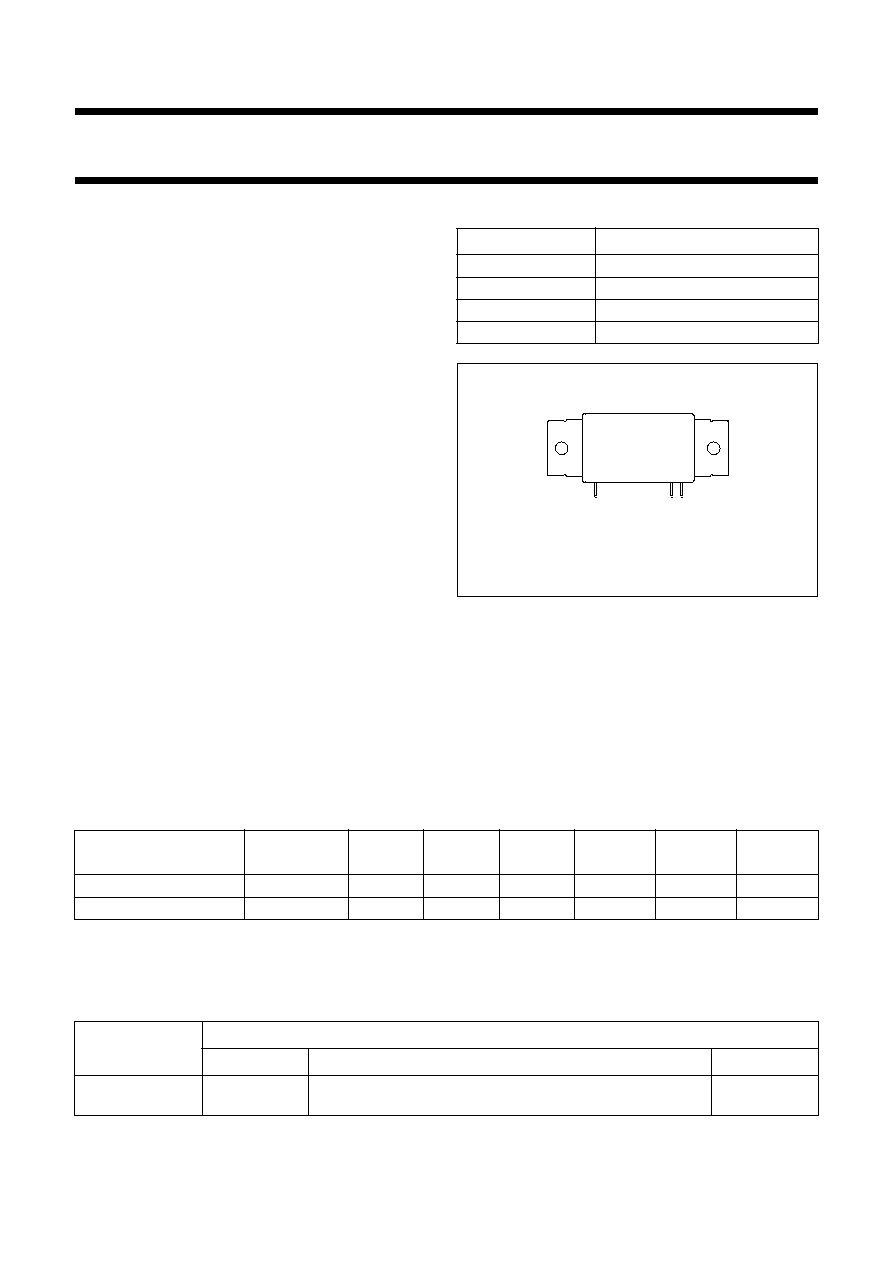
PINNING - SOT365C
PIN
DESCRIPTION
1
RF input
2
V
S
3
RF output
Flange
ground
2 3
1
Top view
MBL257
Fig.1 Simplified outline.
QUICK REFERENCE DATA
Typical RF performance at T
mb
= 25
°
C; Z
S
= Z
L
= 50
.
Note
1. ACPR 400 kHz at 30 kHz resolution bandwidth.
ORDERING INFORMATION
MODE OF OPERATION
f
(MHz)
V
S
(V)
P
L
(W)
G
p
(dB)
(%)
ACPR
(dBc)
rms EVM
(%)
CW
1805 to 1880
26
10
25.5
34
-
-
GSM EDGE
1805 to 1880
26
3.5
26.5
19
-
63
(1)
1.2
TYPE NUMBER
PACKAGE
NAME
DESCRIPTION
VERSION
BGF1801-10
-
plastic rectangular single-ended flat package; flange mounted;
2 mounting holes; 3 in-line leads
SOT365C

2003 Dec 15
3
Philips Semiconductors
Product specification
GSM1800 EDGE power module
BGF1801-10
LIMITING VALUES
In accordance with the Absolute Maximum Rating System (IEC 60134).
CHARACTERISTICS
T
mb
= 25
°
C; V
S
= 26 V; P
L
= 6 W; f = 1805 to 1880 MHz; Z
S
= Z
L
= 50
;
unless otherwise specified.
Notes
1. G
pi
is small signal in-band gain.
2. As defined by ETSI.
SYMBOL
PARAMETER
MIN.
MAX.
UNIT
V
S
DC supply voltage
-
30
V
P
D
input drive power
-
100
mW
P
L
load power
-
15
W
T
stg
storage temperature
-
30
+100
°
C
T
mb
operating mounting base temperature
-
20
+85
°
C
SYMBOL
PARAMETER
CONDITIONS
MIN.
TYP.
MAX.
UNIT
I
DQ
quiescent current (pin 2)
P
D
= 0 mW
220
255
280
mA
P
1dB
load power
at 1 dB gain compression
7
10
-
W
G
p
power gain
24
26.5
29
dB
G
p(freq)
gain flatness over frequency
range
-
0.7
2
dB
G
p(pwr)
gain flatness over power band P
L
= 50 mW up to 5 W
-
1
0
+1
dB
G
OB
out of band gain
small signal, P
D
= 0 dBm;
f < 1805 MHz, f > 1880 MHz
-
-
G
pi max
+ 2
note 1
dB
efficiency
22
25
-
%
VSWR
in
input VSWR
-
1.6 : 1
2.2 : 1
H
2
second harmonic
-
-
58
-
50
dBc
H
3
third harmonic
-
-
59
-
53
dBc
GSM EDGE MODE (P
L
= 3.5 W average)
SR200
spectral regrowth
200 kHz; P
L
= 3.5 W; note 2
-
-
37
-
32
dBc
SR400
400 kHz; P
L
= 3.5 W; note 2
-
-
63
-
60
dBc
EVM
rms
rms EDGE signal distortion
-
1.2
2.5
%
EVM
M
peak EDGE signal distortion
-
3.6
8
%
2003 Dec 15
4
Philips Semiconductors
Product specification
GSM1800 EDGE power module
BGF1801-10
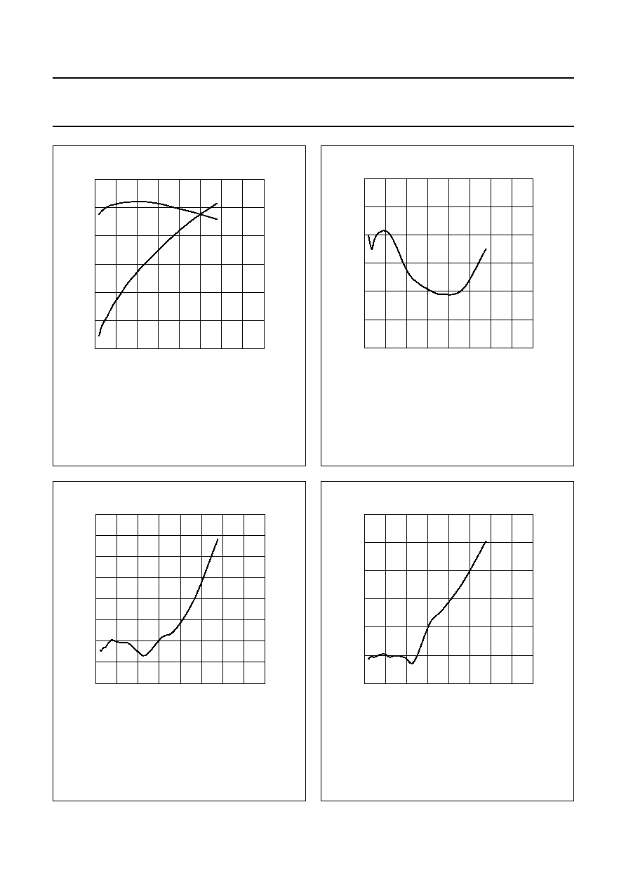
0
P
L(AV)
(W)
27
26
25
24
2
4
8
6
mle335
G
p
(dB)
D
(%)
G
p
D
30
10
20
0
Fig.2
GSM EDGE power gain and efficiency as
functions of load power; typical values.
f = 1843 MHz.
handbook, halfpage
0
PL(AV) (W)
-
61
-
63
-
65
-
67
2
4
8
6
MLE336
ACPR
(dBc)
Fig.3
GSM EDGE ACPR at 400 kHz as a function
of load power; typical values.
f = 1843 MHz.
handbook, halfpage
0
2
PL(AV) W
EVM rms
(%)
4
8
0
2
6
1.5
1
0.5
MLE337
Fig.4
GSM EDGE rms EVM as a function of
average load power; typical values.
f = 1843 MHz.
handbook, halfpage
0
2
PL(AV) (W)
EVM
(%)
4
8
6
2
0
4
6
MLE338
Fig.5
GSM EDGE peak EVM as function of
average load power; typical values.
f = 1843 MHz.
2003 Dec 15
5
Philips Semiconductors
Product specification
GSM1800 EDGE power module
BGF1801-10
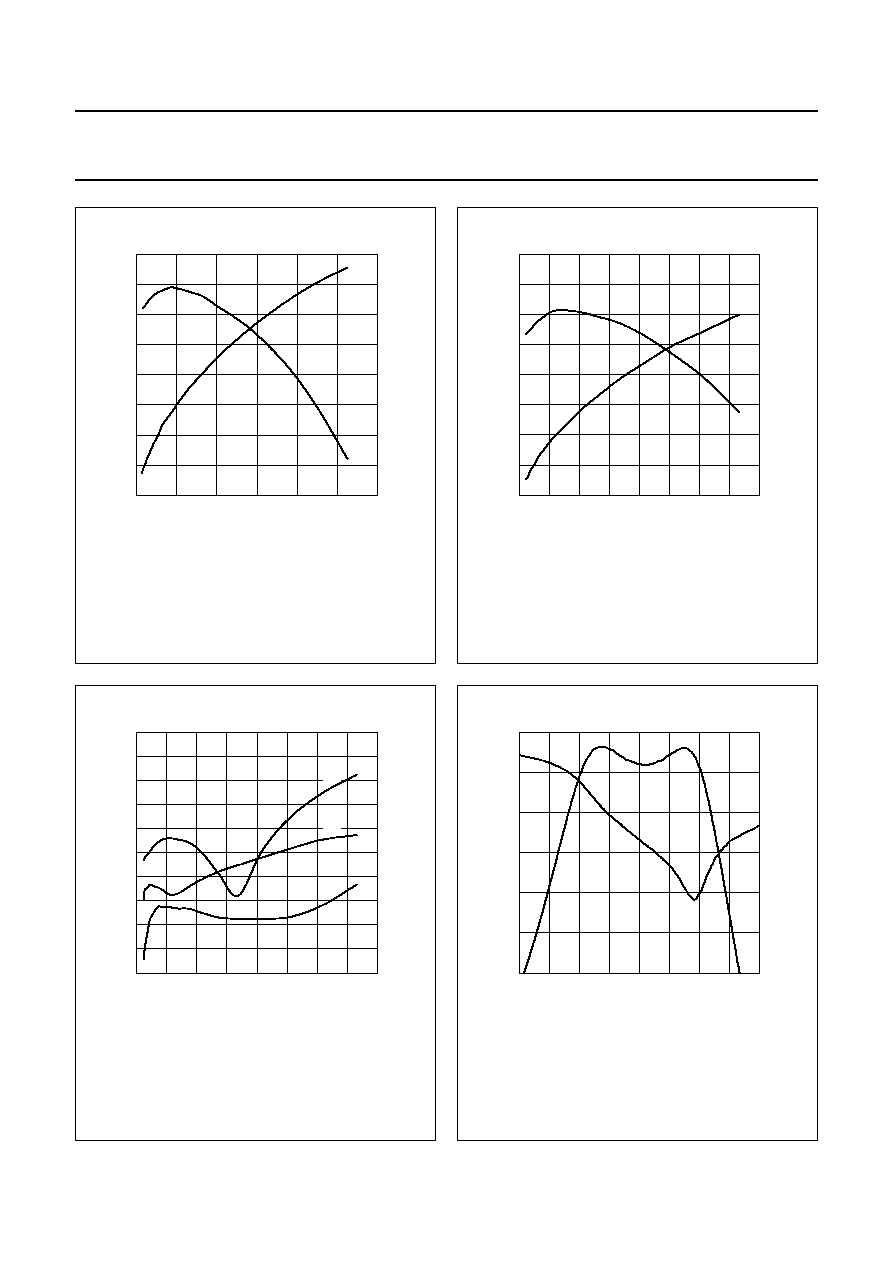
handbook, halfpage
0
5
10
15
26.8
26.4
25.6
25.2
26
40
30
10
0
20
MLE339
Gp
(dB)
Gp
PL (W)
D
(%)
D
Fig.6
CW gain power and efficiency as functions
of load power; typical values.
f = 1843 MHz.
handbook, halfpage
0
2
PL(AV) (W)
Gp
(dB)
4
8
27
26.6
25.8
25.4
26.2
6
MLE340
D
(%)
Gp
D
40
30
10
0
20
Fig.7
Two tone gain power and efficiency as
functions of load power; typical values.
f
1
= 1843 MHz; f
2
= 1843.2 MHz.
handbook, halfpage
0
2
d7
PL(AV) (W)
4
8
-
70
-
30
-
20
6
-
40
-
50
-
60
MLE341
dim
(dBc)
d3
d5
Fig.8
Two tone intermodulation distortion as a
function of average load power; typical
values.
f
1
= 1843 MHz; f
2
= 1843.2 MHz.
handbook, halfpage
1.68
f (GHz)
28
24
20
16
1.76
1.84
2
1.92
MLE342
s21
(dB)
s11
(dB)
s11
s21
0
-
20
-
10
-
30
Fig.9 s-parameters as a function of frequency.
Document Outline