 | –≠–ª–µ–∫—Ç—Ä–æ–Ω–Ω—ã–π –∫–æ–º–ø–æ–Ω–µ–Ω—Ç: BGO847 | –°–∫–∞—á–∞—Ç—å:  PDF PDF  ZIP ZIP |
DATA SHEET
Product specification
Supersedes data of 2000 Jan 04
2000 Apr 12
DISCRETE SEMICONDUCTORS
BGO847; BGO847/FC0;
BGO847/SC0
Optical receiver modules
ook, halfpage
M3D456
2000 Apr 12
2
Philips Semiconductors
Product specification
Optical receiver modules
BGO847; BGO847/FC0;
BGO847/SC0
FEATURES
∑
Improved BGE847BO
∑
Excellent linearity
∑
Extremely low noise up to 870 MHz
∑
Excellent flatness (straight line)
∑
Standard CATV outline
∑
Rugged construction
∑
Gold metallization ensures
excellent reliability
∑
High optical input power range.
APPLICATIONS
∑
CATV optical node systems
operating in the 40 to 870 MHz
frequency range.
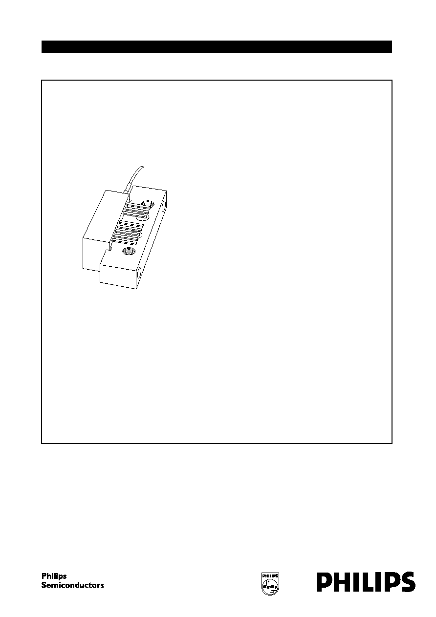
DESCRIPTION
High dynamic range optical receiver
amplifier modules in a standard
SOT115 package where the
non-jacketed fibre has either no
connector or an FC/APC or an
SC/APC connector.
The amplifier supply voltage pin and
the photo diode bias voltage pin both
connect to 24 V (DC).
The modules have a monomode
optical input suitable for
1290 to 1600 nm wavelengths, a
terminal to monitor the photo diode
current and an electrical output
having a characteristic impedance of
75
.
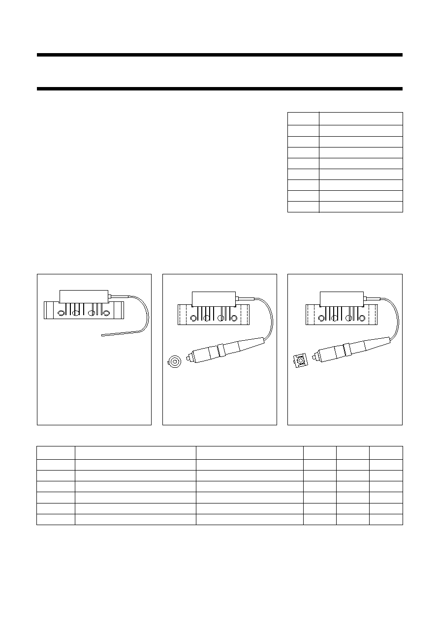
PINNING
PIN
DESCRIPTION
1
monitor current
2
common
3
common
4
+V
B
of the photo diode
5
+V
B
of the amplifier
7
common
8
common
9
output
ge
7
8
9
2
3
4
5
1
Side view
MBK044
Fig.1 Simplified outline
SOT115T
(BGO847).
ok, halfpage
7
8
9
2
3
5
1
Side view
MBL040
4
Fig.2 Simplified outline
SOT115X
(BGO847/FC0).
ok, halfpage
7
8
9
2
4
3
5
1
Side view
MBL041
Fig.3 Simplified outline
SOT115Y
(BGO847/SC0).
QUICK REFERENCE DATA
HANDLING
Fibreglass optical coupling: maximum tensile strength = 5 N; minimum bending radius = 35 mm.
SYMBOL
PARAMETER
CONDITIONS
MIN.
MAX.
UNIT
f
frequency range
40
870
MHz
s
22
output return losses
f = 40 to 870 MHz
11
-
dB
optical input return losses
45
-
dB
d
2
second order distortion
f = 854.5 MHz
-
-
63
dBc
F
equivalent noise input
f = 40 to 750 MHz
-
7
pA/
Hz
I
tot
total current consumption (DC)
V
B
= 24 V
175
205
mA

2000 Apr 12
3
Philips Semiconductors
Product specification
Optical receiver modules
BGO847; BGO847/FC0;
BGO847/SC0
LIMITING VALUES
In accordance with the Absolute Maximum Rating System (IEC 134).
SYMBOL
PARAMETER
CONDITIONS
MIN.
MAX.
UNIT
f
frequency range
40
870
MHz
T
stg
storage temperature
-
40
+85
∞
C
T
mb
operating mounting base temperature
-
20
+85
∞
C
P
in
optical input power
continuous
-
5
mW
ESD
ESD sensitivity
human body model;
R = 1.5 k
; C = 100 pF
500
-
V
CHARACTERISTICS
Bandwidth 40 to 870 MHz; V
B
= 24 V; T
mb
= 30
∞
C; Z
L
= 75
.
SYMBOL
PARAMETER
CONDITIONS
MIN.
MAX.
UNIT
S
responsivity
BGO847
= 1300 nm
800
-
V/W
BGO847/FC0, BGO847/SC0
= 1300 nm
750
-
V/W
FL
flatness straight line
peak to valley; f = 40 to 870 MHz
-
1
dB
SL
slope straight line
f = 40 to 870 MHz
0
2
dB
s
22
output return losses
f = 40 to 870 MHz
11
-
dB
optical input return losses
45
-
dB
d
2
second order distortion
f
m
= 54 MHz; notes 1 and 3
-
-
73
dB
f
m
= 446.5 MHz; notes 1 and 4
-
-
68
dB
f
m
= 548.5 MHz; notes 1 and 5
-
-
67
dB
f
m
= 746.5 MHz; notes 1 and 6
-
-
63
dB
f
m
= 854.5 MHz; notes 1 and 7
-
-
63
dB
d
3
third order distortion
f
m
= 55.25 MHz; notes 2 and 8
-
-
80
dB
f
m
= 445.25 MHz; notes 2 and 9
-
-
75
dB
f
m
= 547.25 MHz; notes 2 and 10
-
-
75
dB
f
m
= 745.25 MHz; notes 2 and 11
-
-
75
dB
f
m
= 853.25 MHz; notes 2 and 12
-
-
73
dB
F
equivalent input noise
f = 40 to 750 MHz
-
7
pA/
Hz
f = 750 to 870 MHz
-
8
pA/
Hz
s
spectral sensitivity
= 1310
±
20 nm
0.85
-
A/W
= 1550
±
20 nm
0.9
-
A/W
optical wavelength
1290
1600
nm
L
length of optical fibre
BGO847
fibre; SM type; 9/125
µ
m
1
-
m
BGO847/FC0, BGO847/SC0
fibre; SM type; 9/125
µ
m
746
861
mm
I
tot
total current consumption (DC)
175
205
mA
I
pin 4
pin diode bias current (DC)
-
25
mA

2000 Apr 12
4
Philips Semiconductors
Product specification
Optical receiver modules
BGO847; BGO847/FC0;
BGO847/SC0
Notes
1. Two laser test; each laser with 40% modulation index; P
opt
= 1 mW (total).
2. Three laser test; each laser with 60% modulation index; P
opt
= 1 mW (total).
3. f
m
= 54 MHz; f
p
= 187.25 MHz; f
q
= 133.25 MHz.
4. f
m
= 446.5 MHz; f
p
= 97.25 MHz; f
q
= 349.25 MHz.
5. f
m
= 548 .5MHz; f
p
= 109.25 MHz; f
q
= 439.25 MHz.
6. f
m
= 746.5 MHz; f
p
= 133.25 MHz; f
q
= 613.25 MHz.
7. f
m
= 854.5 MHz; f
p
= 133.25 MHz; f
q
= 721.25 MHz.
8. f
m
= 55.25 MHz; f
p
= 109.25 MHz; f
q
= 133.25 MHz f
r
= 187.25 MHz.
9. f
m
= 445.25 MHz; f
p
= 193.25 MHz; f
q
= 349.25 MHz f
r
= 97.25 MHz.
10. f
m
= 547.25 MHz; f
p
= 217.25 MHz; f
q
= 439.25 MHz f
r
= 109.25 MHz.
11. f
m
= 745.25 MHz; f
p
= 133.25 MHz; f
q
= 265.25 MHz f
r
= 613.25 MHz.
12. f
m
= 853.25 MHz; f
p
= 133.25 MHz; f
q
= 265.25 MHz f
r
= 721.25 MHz.
Fig.4 Monitor current pin.
handbook, halfpage
MLB151
10 k
1 k
Pin 1
photo
current

2000 Apr 12
5
Philips Semiconductors
Product specification
Optical receiver modules
BGO847; BGO847/FC0;
BGO847/SC0
PACKAGE OUTLINES
UNIT
A2
max.
c
e
e1
q
Q
max.
q1
q2
U1
max.
U2
W
REFERENCES
OUTLINE
VERSION
EUROPEAN
PROJECTION
ISSUE DATE
IEC
JEDEC
EIAJ
mm
20.8
9.1
0.51
0.38
0.25 27.2 2.54 13.75 2.54 5.08 12.7
8.8
1000
4.15
3.85
2.4
38.1 25.4 10.2
4.2
44.75
8
0.25
0.1
12
b
F
2.5
M
1.6
M1
0.9
M2
N
min.
10.7
8.7
N1
5
1
N2
16.7
16.1
optical input
S1
4.95
4.55
S2
p
6-32
UNC
y
w
S
DIMENSIONS (mm are the original dimensions)
SOT115T
0
5
10 mm
scale
A
max.
D
max.
d
max.
L
min.
E
max.
Z
max.
Rectangular single-ended package; aluminium flange; 2 vertical mounting holes;
2 x 6-32 UNC and 2 extra horizontal mounting holes; optical input; 8 gold-plated in-line leads
SOT115T
D
U1
q
q2
q1
b
F
S
S1
S2
A
Z
p
N
N1
N2
M
M1
M2
E
A2
L
c
d
Q
U2
M
w
7
8
9
2
3
4
W
e
e1
5
p
1
y
M
B
y
M
B
y
M
B
B
99-04-13