 | –≠–ª–µ–∫—Ç—Ä–æ–Ω–Ω—ã–π –∫–æ–º–ø–æ–Ω–µ–Ω—Ç: BGY685A | –°–∫–∞—á–∞—Ç—å:  PDF PDF  ZIP ZIP |

DATA SHEET
Product specification
Supersedes data of 1997 Apr 21
File under Discrete Semiconductors, SC16
1998 Mar 16
DISCRETE SEMICONDUCTORS
BGY685A
CATV amplifier module
book, halfpage
M3D252

1998 Mar 16
2
Philips Semiconductors
Product specification
CATV amplifier module
BGY685A
FEATURES
∑
Excellent linearity
∑
Extremely low noise
∑
Silicon nitride passivation
∑
Rugged construction
∑
Gold metallization ensures excellent reliability.
DESCRIPTION
Special super-high dynamic range amplifier module
designed for applications in CATV systems with a
bandwidth of 40 to 600 MHz operating at a voltage supply
of 24 V (DC).
PINNING - SOT115J
PIN
DESCRIPTION
1
input
2
common
3
common
5
+V
B
7
common
8
common
9
output
Fig.1 Simplified outline.
handbook, halfpage
7
8
9
2
3
5
1
Side view
MSA319
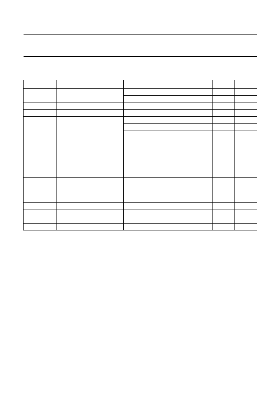
QUICK REFERENCE DATA
LIMITING VALUES
In accordance with the Absolute Maximum Rating System (IEC 134).
SYMBOL
PARAMETER
CONDITIONS
MIN.
TYP.
MAX.
UNIT
G
p
power gain
f = 50 MHz
17.7
-
18.7
dB
f = 600 MHz
19
-
-
dB
I
tot
total current consumption (DC)
V
B
= 24 V
-
220
240
mA
SYMBOL
PARAMETER
MIN.
MAX.
UNIT
V
i
RF input voltage
-
65
dBmV
T
stg
storage temperature
-
40
+100
∞
C
T
mb
mounting base operating temperature
-
20
+100
∞
C
1998 Mar 16
3
Philips Semiconductors
Product specification
CATV amplifier module
BGY685A
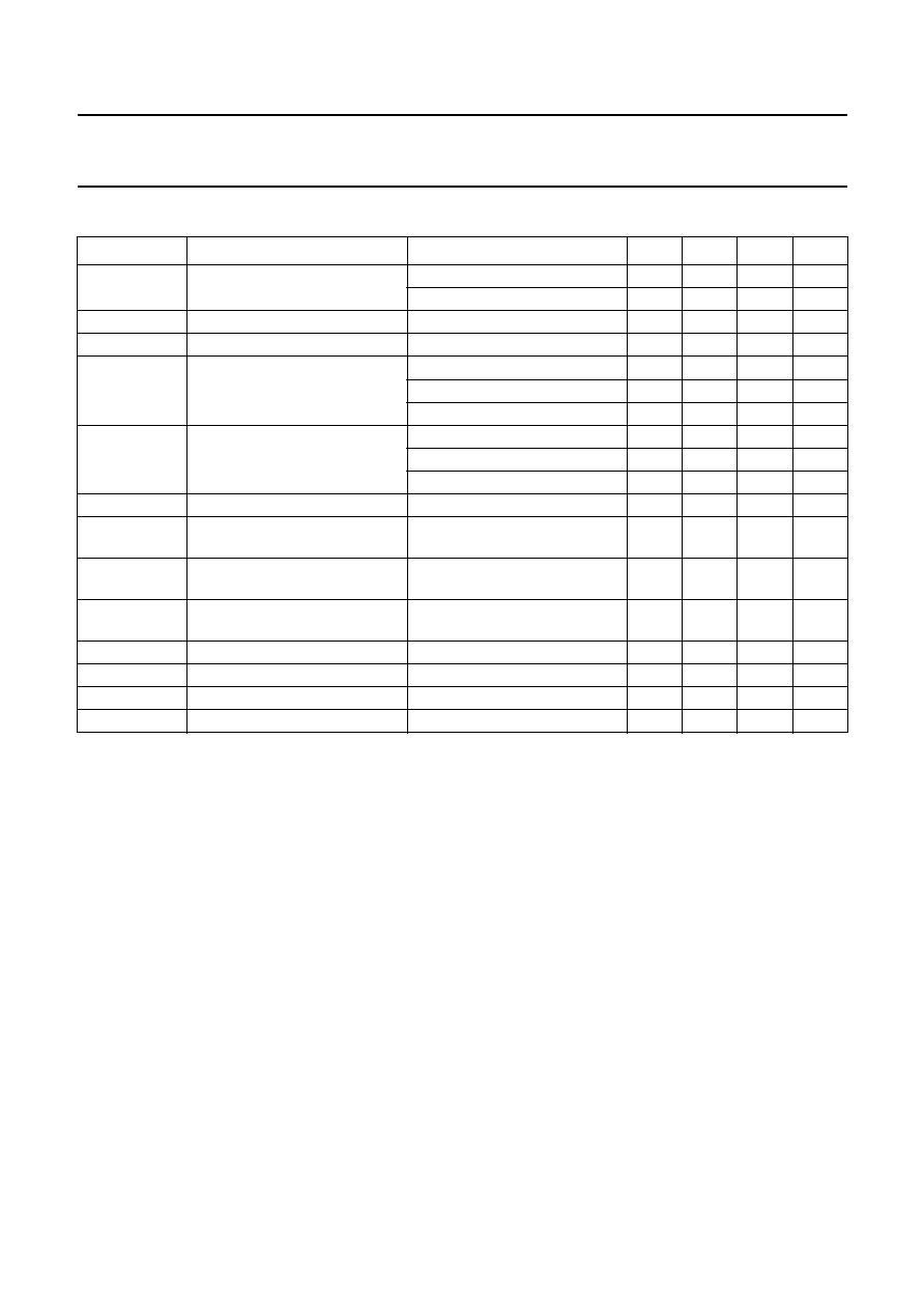
CHARACTERISTICS
Table 1
Bandwidth 40 to 600 MHz; T
case
= 30
∞
C; Z
S
= Z
L
= 75
Notes
1. f
p
= 55.25 MHz; V
p
= 44 dBmV;
f
q
= 541.25 MHz; V
q
= 44 dBmV;
measured at f
p
+ f
q
= 596.5 MHz.
2. f
p
= 590.25 MHz; V
p
= V
o
;
f
q
= 597.25 MHz; V
q
= V
o
-
6 dB;
f
r
= 599.25 MHz; V
r
= V
o
-
6 dB;
measured at f
p
+ f
q
-
f
r
= 588.25 MHz.
3. The module normally operates at V
B
= 24 V, but is able to withstand supply transients up to 30 V.
SYMBOL
PARAMETER
CONDITIONS
MIN.
MAX.
UNIT
G
p
power gain
f = 50 MHz
17.7
18.7
dB
f = 600 MHz
19
-
dB
SL
slope cable equivalent
f = 40 to 600 MHz
0.5
2.2
dB
FL
flatness of frequency response
f = 40 to 600 MHz
-
±
0.2
dB
S
11
input return losses
f = 40 to 80 MHz
20
-
dB
f = 80 to 160 MHz
19
-
dB
f = 160 to 600 MHz
18
-
dB
S
22
output return losses
f = 40 to 80 MHz
20
-
dB
f = 80 to 160 MHz
19
-
dB
f = 160 to 600 MHz
18
-
dB
S
21
phase response
f = 50 MHz
-
45
+45
deg
CTB
composite triple beat
85 channels flat; V
o
= 44 dBmV;
measured at 595.25 MHz
-
-
55
dB
X
mod
cross modulation
85 channels flat; V
o
= 44 dBmV;
measured at 55.25 MHz
-
-
60
dB
CSO
composite second order
distortion
85 channels flat; V
o
= 44 dBmV;
measured at 596.5 MHz
-
-
56
dB
d
2
second order distortion
note 1
-
-
70
dB
V
o
output voltage
d
im
=
-
60 dB; note 2
60
-
dBmV
F
noise figure
f = 600 MHz
-
8.5
dB
I
tot
total current consumption (DC)
note 3
-
240
mA

1998 Mar 16
4
Philips Semiconductors
Product specification
CATV amplifier module
BGY685A
Table 2
Bandwidth 40 to 550 MHz; T
case
= 30
∞
C; Z
S
= Z
L
= 75
Notes
1. f
p
= 55.25 MHz; V
p
= 44 dBmV;
f
q
= 493.25 MHz; V
q
= 44 dBmV;
measured at f
p
+ f
q
= 548.5 MHz.
2. f
p
= 540.25 MHz; V
p
= V
o
;
f
q
= 547.25 MHz; V
q
= V
o
-
6 dB;
f
r
= 549.25 MHz; V
r
= V
o
-
6 dB;
measured at f
p
+ f
q
-
f
r
= 538.25 MHz.
3. The module normally operates at V
B
= 24 V, but is able to withstand supply transients up to 30 V.
SYMBOL
PARAMETER
CONDITIONS
MIN.
TYP.
MAX.
UNIT
G
p
power gain
f = 50 MHz
17.7
-
18.7
dB
f = 550 MHz
18.8
-
20
dB
SL
slope cable equivalent
f = 40 to 550 MHz
0.5
-
2
dB
FL
flatness of frequency response
f = 40 to 550 MHz
-
-
±
0.2
dB
S
11
input return losses
f = 40 to 80 MHz
20
-
-
dB
f = 80 to 160 MHz
19
-
-
dB
f = 160 to 550 MHz
18
-
-
dB
S
22
output return losses
f = 40 to 80 MHz
20
-
-
dB
f = 80 to 160 MHz
19
-
-
dB
f = 160 to 550 MHz
18
-
-
dB
S
21
phase response
f = 50 MHz
-
45
-
+45
deg
CTB
composite triple beat
77 channels flat; V
o
= 44 dBmV;
measured at 547.25 MHz
-
-
-
59
dB
X
mod
cross modulation
77 channels flat; V
o
= 44 dBmV;
measured at 55.25 MHz
-
-
-
62
dB
CSO
composite second order
distortion
77 channels flat; V
o
= 44 dBmV;
measured at 548.5 MHz
-
-
-
59
dB
d
2
second order distortion
note 1
-
-
-
72
dB
V
o
output voltage
d
im
=
-
60 dB; note 2
61.5
-
-
dBmV
F
noise figure
f = 550 MHz
-
-
8
dB
I
tot
total current consumption (DC)
note 3
-
220
240
mA
1998 Mar 16
5
Philips Semiconductors
Product specification
CATV amplifier module
BGY685A
Table 3
Bandwidth 40 to 450 MHz; T
case
= 30
∞
C; Z
S
= Z
L
= 75
Notes
1. f
p
= 55.25 MHz; V
p
= 46 dBmV;
f
q
= 391.25 MHz; V
q
= 46 dBmV;
measured at f
p
+ f
q
= 446.5 MHz.
2. f
p
= 440.25 MHz; V
p
= V
o
;
f
q
= 447.25 MHz; V
q
= V
o
-
6 dB;
f
r
= 449.25 MHz; V
r
= V
o
-
6 dB;
measured at f
p
+ f
q
-
f
r
= 438.25 MHz.
3. The module normally operates at V
B
= 24 V, but is able to withstand supply transients up to 30 V.
SYMBOL
PARAMETER
CONDITIONS
MIN.
TYP.
MAX.
UNIT
G
p
power gain
f = 50 MHz
17.7
-
18.7
dB
f = 450 MHz
18.6
-
19.8
dB
SL
slope cable equivalent
f = 40 to 450 MHz
0.5
-
1.8
dB
FL
flatness of frequency response
f = 40 to 450 MHz
-
-
±
0.2
dB
S
11
input return losses
f = 40 to 80 MHz
20
-
-
dB
f = 80 to 160 MHz
19
-
-
dB
f = 160 to 450 MHz
18
-
-
dB
S
22
output return losses
f = 40 to 80 MHz
20
-
-
dB
f = 80 to 160 MHz
19
-
-
dB
f = 160 to 450 MHz
18
-
-
dB
S
21
phase response
f = 50 MHz
-
45
-
+45
deg
CTB
composite triple beat
60 channels flat; V
o
= 46 dBmV;
measured at 445.25 MHz
-
-
-
61
dB
X
mod
cross modulation
60 channels flat; V
o
= 46 dBmV;
measured at 55.25 MHz
-
-
-
61
dB
CSO
composite second order
distortion
60 channels flat; V
o
= 46 dBmV;
measured at 446.5 MHz
-
-
-
61
dB
d
2
second order distortion
note 1
-
-
-
75
dB
V
o
output voltage
d
im
=
-
60 dB; note 2
64
-
-
dBmV
F
noise figure
f = 450 MHz
-
-
7
dB
I
tot
total current consumption (DC)
note 3
-
220
240
mA