Document Outline
- FEATURES
- APPLICATIONS
- DESCRIPTION
- QUICK REFERENCE DATA
- PINNING - SOT608A
- LIMITING VALUES
- THERMAL CHARACTERISTICS
- CHARACTERISTICS
- APPLICATION INFORMATION
- PACKAGE OUTLINE
- DATA SHEET STATUS
- DEFINITIONS
- DISCLAIMERS
DATA SHEET
Product specification
Supersedes data of 2002 Dec 19
2003 Feb 24
DISCRETE SEMICONDUCTORS
BLF2022-30
UHF power LDMOS transistor
M3D750
2003 Feb 24
2
Philips Semiconductors
Product specification
UHF power LDMOS transistor
BLF2022-30
FEATURES
∑
Typical W-CDMA performance at a supply voltage of
28 V and I
DQ
of 240 mA:
≠ Output power = 3.5 W (AV)
≠ Gain = 12.9 dB
≠ Efficiency = 16.5%
≠ ACPR =
-
45 dBc at 3.84 MHz
≠ d
im
=
-
42 dBc
∑
Easy power control
∑
Excellent ruggedness
∑
High power gain
∑
Excellent thermal stability
∑
Designed for broadband operation (2000 to 2200 MHz)
∑
Internally matched for ease of use.
APPLICATIONS
∑
RF power amplifiers for W-CDMA base stations and
multicarrier applications in the 2000 to 2200 MHz
frequency range.
DESCRIPTION
30 W LDMOS power transistor for base station
applications at frequencies from 2000 to 2200 MHz.
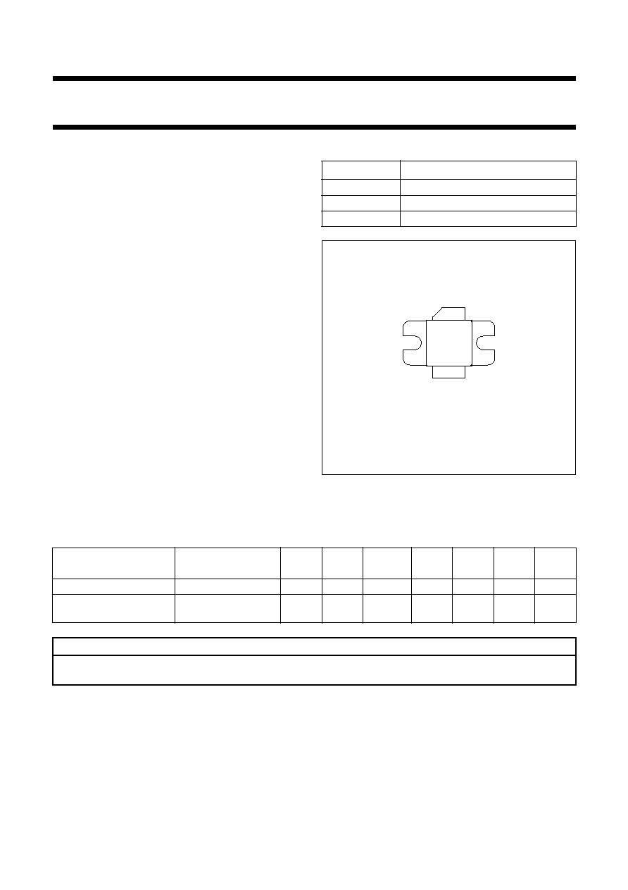
PINNING - SOT608A
PIN
DESCRIPTION
1
drain
2
gate
3
source, connected to flange
Top view
2
1
3
MBL290
Fig.1 Simplified outline (SOT608A).
QUICK REFERENCE DATA
Typical RF performance at T
h
= 25
∞
C in a common source test circuit.
MODE OF OPERATION
f
(MHz)
V
DS
(V)
I
DQ
(mA)
P
L
(W)
G
p
(dB)
D
(%)
d
im
(dBc)
ACLR
5
(dBc)
2-tone, class-AB
f
1
= 2170; f
2
= 2170.1
28
240
30 (PEP)
12.6
34.3
-
29.5
-
two-carrier W-CDMA test
model 1, 64 channels
f
1
= 2155; f
2
= 2165
28
270
3.5 (AV)
12.9
16.5
-
42
-
45
CAUTION
This product is supplied in anti-static packing to prevent damage caused by electrostatic discharge during transport
and handling. For further information, refer to Philips specs.: SNW-EQ-608, SNW-FQ-302A and SNW-FQ-302B.
2003 Feb 24
3
Philips Semiconductors
Product specification
UHF power LDMOS transistor
BLF2022-30
LIMITING VALUES
In accordance with the Absolute Maximum Rating System (IEC 60134).
THERMAL CHARACTERISTICS
Notes
1. Thermal resistance is determined under specified RF operating conditions.
CHARACTERISTICS
T
j
= 25
∞
C unless otherwise specified.
APPLICATION INFORMATION
RF performance in a common source class-AB circuit. T
h
= 25
∞
C; R
th j-c
= 1.85 K/W; unless otherwise specified.
Ruggedness in class-AB operation
The BLF2022-30 is capable of withstanding a load mismatch corresponding to VSWR = 10 : 1 through all phases under
the following conditions: V
DS
= 28 V; I
DQ
= 240 mA; P
L
= 30 W; f = 2170 MHz.
SYMBOL
PARAMETER
MIN.
MAX.
UNIT
V
DS
drain-source voltage
-
65
V
V
GS
gate-source voltage
-
±
15
V
I
D
DC drain current
-
4.5
A
T
stg
storage temperature
-
65
+150
∞
C
T
j
junction temperature
-
200
∞
C
SYMBOL
PARAMETER
CONDITIONS
VALUE
UNIT
R
th j-h
thermal resistance from junction to heatsink T
h
= 25
∞
C; note 1
1.85
K/W
SYMBOL
PARAMETER
CONDITIONS
MIN.
TYP.
MAX.
UNIT
V
(BR)DSS
drain-source breakdown voltage
V
GS
= 0; I
D
= 0.7 mA
65
-
-
V
V
GSth
gate-source threshold voltage
V
DS
= 10 V; I
D
= 70 mA
4.5
-
5.5
V
I
DSS
drain-source leakage current
V
GS
= 0; V
DS
= 28 V
-
-
5
µ
A
I
DSX
on-state drain current
V
GS
= V
GSth
+ 9 V; V
DS
= 10 V
9
-
-
A
I
GSS
gate leakage current
V
GS
=
±
15 V; V
DS
= 0
-
-
11
nA
g
fs
forward transconductance
V
DS
= 10 V; I
D
= 2.5 A
-
2
-
S
R
DSon
drain-source on-state resistance
V
GS
= V
GSth
+ 9 V; I
D
= 2.5 A
-
0.3
-
C
rs
feedback capacitance
V
GS
= 0; V
DS
= 28 V; f = 1 MHz
-
1.7
-
pF
MODE OF OPERATION
f
(MHz)
V
DS
(V)
I
DQ
(mA)
P
L
(W)
G
p
(dB)
D
(%)
d
im
(dBc)
2-tone, class-AB
f
1
= 2170; f
2
= 2170.1
28
240
30 (PEP)
>11
>30
-
25

2003 Feb 24
4
Philips Semiconductors
Product specification
UHF power LDMOS transistor
BLF2022-30
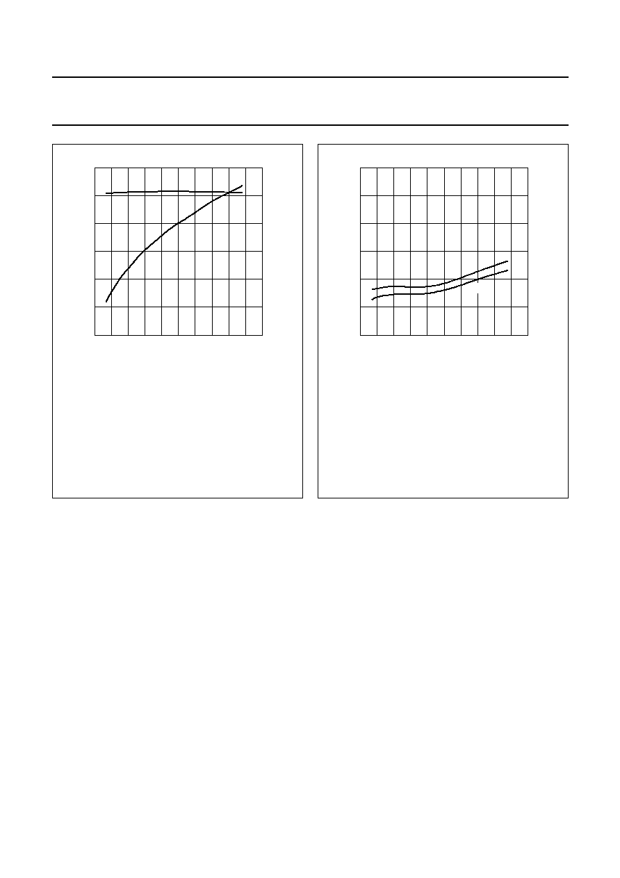
handbook, halfpage
Gp
(dB)
Gp
D
(%)
D
15
10
5
0
60
20
0
40
MLD935
0
20
10
30
40
50
PL (PEP) (W)
Fig.2
Power gain and drain efficiency as functions
of peak envelope load power; typical
values.
V
DS
= 28 V; I
DQ
= 240 mA; T
h
25
∞
C;
f
1
= 2170 MHz; f
2
= 2170.1 MHz.
handbook, halfpage
dim
(dBc)
d3
d5
d7
0
20
10
30
40
50
PL (PEP) (W)
0
-
20
-
60
-
80
-
40
MLD936
V
DS
= 28 V; I
DQ
= 240 mA; T
h
25
∞
C;
f
1
= 2170 MHz; f
2
= 2170.1 MHz.
Fig.3
Intermodulation distortion as a function of
peak envelope load power; typical values.
handbook, halfpage
Gp
(dB)
D
(%)
15
10
5
0
60
20
0
40
MLD937
0
20
10
30
40
50
PL (PEP) (W)
(1)
(3)
(2)
(4)
(6)
(5)
Gp
D
Fig.4
Power gain and drain efficiency as functions
of peak envelope load power; typical
values.
V
DS
= 28 V; T
h
25
∞
C;
f
1
= 2170 MHz; f
2
= 2170.1 MHz.
(1) I
DQ
= 290 mA.
(2) I
DQ
= 240 mA.
(3) I
DQ
= 190 mA.
(4) I
DQ
= 190 mA.
(5) I
DQ
= 240 mA.
(6) I
DQ
= 290 mA.
handbook, halfpage
dim
(dBc)
0
20
10
30
40
50
PL (PEP) (W)
0
-
20
-
60
-
80
-
40
MLD938
(2)
(3)
(1)
V
DS
= 28 V; T
h
25
∞
C;
f
1
= 2170 MHz; f
2
= 2170.1 MHz.
Fig.5
Third order intermodulation distortion as a
function of peak envelope load power;
typical values.
(1) I
DQ
= 190 mA.
(2) I
DQ
= 240 mA.
(3) I
DQ
= 290 mA.
2003 Feb 24
5
Philips Semiconductors
Product specification
UHF power LDMOS transistor
BLF2022-30
handbook, halfpage
Gp
(dB)
Gp
D
(%)
D
15
10
5
0
30
10
0
20
MLD940
0
4
2
6
8
10
PL (AV) (W)
Fig.6
Power gain and drain efficiency as functions
of average load power; typical values.
Two-carrier W-CDMA performance.
V
DS
= 28 V; I
DQ
= 270 mA; T
h
25
∞
C; f
1
= 2170 MHz.
Input signal: 3GPP W-CDMA 64 channels with 66% clipping;
peak to average power ratio: 8.5 dB at 0.01% probability on CCDF;
channel spacing/bandwidth = 5 MHz / 3.84 MHz.
handbook, halfpage
dim
(dBc)
ACLR
(dBc)
0
4
2
6
8
10
0
-
20
-
60
-
40
0
-
20
-
60
-
40
MLD941
ACLR
dim
PL (AV) (W)
Fig.7
Intermodulation distortion and adjacent
channel leakage ratio (ACLR) as functions
of average load power; typical values.
Two-carrier W-CDMA performance.
V
DS
= 28 V; I
DQ
= 270 mA; T
h
25
∞
C; f
1
= 2155 MHz;
f
1
= 2165 MHz;.
Input signal: 3GPP W-CDMA 64 channels with 66% clipping;
peak to average power ratio: 8.5 dB at 0.01% probability on CCDF;
channel spacing/bandwidth = 5 MHz / 3.84 MHz.