Document Outline
- FEATURES
- APPLICATIONS
- DESCRIPTION
- PINNING
- QUICK REFERENCE DATA
- LIMITING VALUES
- THERMAL CHARACTERISTICS
- CHARACTERISTICS
- APPLICATION INFORMATION
- PACKAGE OUTLINE
- DATA SHEET STATUS
- DEFINITIONS
- DISCLAIMERS
DATA SHEET
Preliminary specification
2001 April 05
DISCRETE SEMICONDUCTORS
BLF2022-40
UHF power LDMOS transistor
M3D750

2001 April 05
2
Philips Semiconductors
Preliminary specification
UHF power LDMOS transistor
BLF2022-40
FEATURES
∑ High power gain
∑ Easy power control
∑ Excellent ruggedness
∑ Designed for broadband operation (2.0 to 2.2 GHz)
∑ Internal input and output matching for high gain and
efficiency
∑ Improved linearity at backoff levels.
APPLICATIONS
∑ Common source class-AB operation for PCN and PCS
applications in the 2000 to 2200 MHz frequency range
∑ Suitable for GSM, Edge, CDMA and WCDMA
applications.
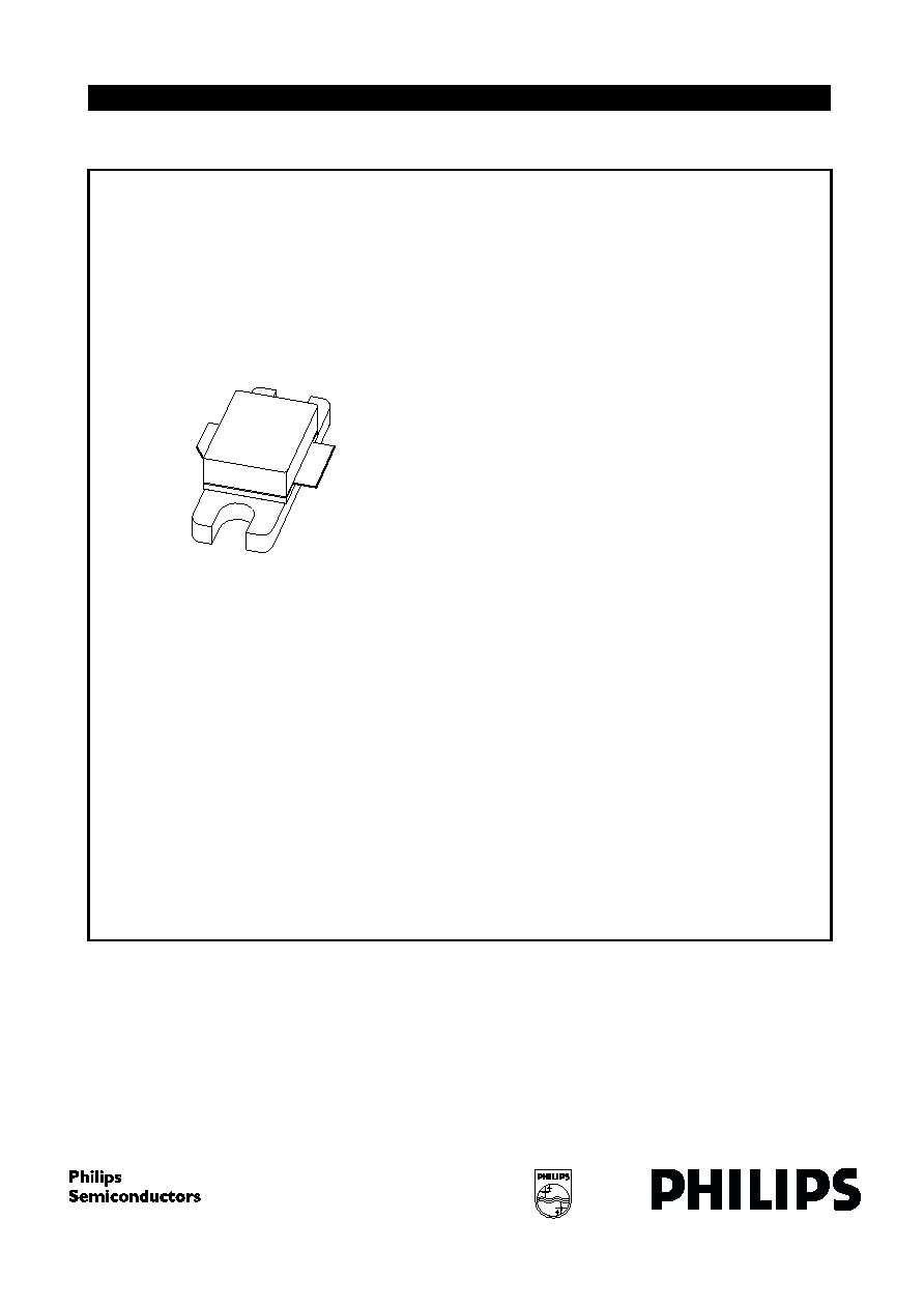
DESCRIPTION
Silicon N-channel enhancement mode lateral D-MOS
transistors encapsulated in a 2-lead SOT608A flange
package with a ceramic cap. The common source is
connected to the mounting flange.
PINNING
PIN
DESCRIPTION
1
drain
2
gate
3
source, connected to flange
Top view
2
1
3
MBL290
Fig.1 Simplified outline SOT608A.
QUICK REFERENCE DATA
RF performance at T
h
= 25
∞C in a common source test circuit.
LIMITING VALUES
In accordance with the Absolute Maximum Rating System (IEC 134).
MODE OF OPERATION
f
(MHz)
V
DS
(V)
P
L
(W)
G
p
(dB)
D
(%)
d
im
(dBc)
Two-tone, class-AB
f
1
= 2170; f
2
= 2170.1
28
40 (PEP)
>10.5
>30
-25
SYMBOL
PARAMETER
MIN.
MAX.
UNIT
V
DS
drain-source voltage
-
65
V
V
GS
gate-source voltage
-
±15
V
I
D
DC drain current
-
5
A
T
stg
storage temperature
-65
+150
∞C
T
j
junction temperature
-
200
∞C
2001 April 05
3
Philips Semiconductors
Preliminary specification
UHF power LDMOS transistor
BLF2022-40
THERMAL CHARACTERISTICS
Note
1.
Determined under specified RF operating conditions.
CHARACTERISTICS
T
j
= 25
∞C unless otherwise specified.
APPLICATION INFORMATION
RF performance in a common source class-AB circuit. T
h
= 25
∞C; R
th j-h
= 1.15 K/W, unless otherwise specified.
Ruggedness in class-AB operation
The BLF2022-40 is capable of withstanding a load mismatch corresponding to VSWR = 10 : 1 through all phases under
the following conditions: V
DS
= 28 V; I
DQ
= 340 mA; P
L
= 40 W; f = 2170 MHz.
SYMBOL
PARAMETER
CONDITIONS
VALUE
UNIT
R
th j-h
thermal resistance from junction to
heatsink
T
h
= 25
∞C, P
tot
= 152 W, note 1
2.3
K/W
SYMBOL
PARAMETER
CONDITIONS
MIN.
TYP.
MAX.
UNIT
V
(BR)DSS
drain-source breakdown voltage
V
GS
= 0; I
D
= 0.8 mA
65
-
-
V
V
GSth
gate-source threshold voltage
V
DS
= 10 V; I
D
= 80 mA
-
5
-
V
I
DSS
drain-source leakage current
V
GS
= 0; V
DS
= 26 V
-
-
6
µA
I
DSX
on-state drain current
V
GS
= V
GS th
+ 9 V; V
DS
= 10 V
11
-
-
A
I
GSS
gate leakage current
V
GS
=
±15 V; V
DS
= 0
-
-
14
nA
g
fs
forward transconductance
V
DS
= 10 V; I
D
= 2.9 A
-
2.3
-
S
R
DSon
drain-source on-state resistance
V
GS
= V
GS th
+ 9 V; I
D
= 2.9 A
-
0.26
-
C
rss
feedback capacitance
V
GS
= 0; V
DS
= 26 V; f = 1 MHz
-
1.7
-
pF
MODE OF OPERATION
f
(MHz)
V
DS
(V)
I
DQ
(mA)
P
L
(W)
G
p
(dB)
D
(%)
d
im
(dBc)
Two-tone, class-AB
f
1
= 2170; f
2
= 2170.1
28
340
40 (PEP)
>10.5
>30
-25
2001 April 05
4
Philips Semiconductors
Preliminary specification
UHF power LDMOS transistor
BLF2022-40
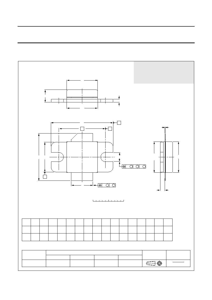
PACKAGE OUTLINE
Package under
development
Philips Semiconductors reserves the
right to make changes without notice.
REFERENCES
OUTLINE
VERSION
EUROPEAN
PROJECTION
ISSUE DATE
IEC
JEDEC
EIAJ
SOT608A
01-02-02
01-02-22
0
5
10 mm
scale
Flanged ceramic package; 2 mounting holes; 2 leads
SOT608A
p
A
F
b
D
U2
H
Q
c
1
3
2
D1
E
A
w1
A
B
M
M
M
C
q
U1
C
B
E1
M
M
w2
UNIT
A
mm
D
b
7.24
6.99
0.15
0.10
10.29
9.98
10.29
10.03
15.75
14.73
9.91
9.65
4.75
3.73
c
U2
0.25
0.51
15.24
q
w2
w1
F
1.14
0.89
U1
20.45
20.19
p
3.43
3.18
Q
1.70
1.35
E
E1
10.29
9.98
inches
0.285
0.275
0.006
0.004
0.405
0.393
D1
10.29
10.03
0.405
0.395
0.405
0.395
0.620
0.580
0.390
0.380
0.187
0.147
0.010
0.020
0.600
0.045
0.035
0.805
0.795
0.125
0.115
0.067
0.053
0.405
0.393
H
DIMENSIONS (millimetre dimensions are derived from the original inch dimensions)

2001 April 05
5
Philips Semiconductors
Preliminary specification
UHF power LDMOS transistor
BLF2022-40
DATA SHEET STATUS
Notes
1.
Please consult the most recently issued data sheet before initiating or completing a design.
2.
The product status of the device(s) described in this data sheet may have changed since this data sheet was
published. The latest information is available on the Internet at URL http://www.semiconductors.philips.com.
DATA SHEET
STATUS
(1)
PRODUCT
STATUS
(2)
DEFINITIONS
Objective data
Development
This data sheet contains data from the objective specification for product
development. Philips Semiconductors reserves the right to change the
specification in any manner without notice.
Preliminary data
Qualification
This data sheet contains data from the preliminary specification.
Supplementary data will be published at a later date. Philips
Semiconductors reserves the right to change the specification without
notice, in order to improve the design and supply the best possible
product.
Product data
Production
This data sheet contains data from the product specification. Philips
Semiconductors reserves the right to make changes at any time in order
to improve the design, manufacturing and supply. Changes will be
communicated according to the Customer Product/Process Change
Notification (CPCN) procedure SNW-SQ-650A.
DEFINITIONS
Short-form specification
The data in a short-form
specification is extracted from a full data sheet with the
same type number and title. For detailed information see
the relevant data sheet or data handbook.
Limiting values definition
Limiting values given are in
accordance with the Absolute Maximum Rating System
(IEC 60134). Stress above one or more of the limiting
values may cause permanent damage to the device.
These are stress ratings only and operation of the device
at these or at any other conditions above those given in the
Characteristics sections of the specification is not implied.
Exposure to limiting values for extended periods may
affect device reliability.
Application information
Applications that are
described herein for any of these products are for
illustrative purposes only. Philips Semiconductors make
no representation or warranty that such applications will be
suitable for the specified use without further testing or
modification.
DISCLAIMERS
Life support applications
These products are not
designed for use in life support appliances, devices, or
systems where malfunction of these products can
reasonably be expected to result in personal injury. Philips
Semiconductors customers using or selling these products
for use in such applications do so at their own risk and
agree to fully indemnify Philips Semiconductors for any
damages resulting from such application.
Right to make changes
Philips Semiconductors
reserves the right to make changes, without notice, in the
products, including circuits, standard cells, and/or
software, described or contained herein in order to
improve design and/or performance. Philips
Semiconductors assumes no responsibility or liability for
the use of any of these products, conveys no licence or title
under any patent, copyright, or mask work right to these
products, and makes no representations or warranties that
these products are free from patent, copyright, or mask
work right infringement, unless otherwise specified.
CAUTION
This product is supplied in anti-static packing to prevent damage caused by electrostatic discharge during transport
and handling. For further information, refer to Philips specs.: SNW-EQ-608, SNW-FQ-302A and SNW-FQ-302B.