 | –≠–ª–µ–∫—Ç—Ä–æ–Ω–Ω—ã–π –∫–æ–º–ø–æ–Ω–µ–Ω—Ç: BLF245 | –°–∫–∞—á–∞—Ç—å:  PDF PDF  ZIP ZIP |

DATA SHEET
Product specification
September 1992
DISCRETE SEMICONDUCTORS
BLF245
VHF power MOS transistor
September 1992
2
Philips Semiconductors
Product specification
VHF power MOS transistor
BLF245
FEATURES
∑
High power gain
∑
Low noise figure
∑
Easy power control
∑
Good thermal stability
∑
Withstands full load mismatch.
DESCRIPTION
Silicon N-channel enhancement
mode vertical D-MOS transistor
designed for large signal amplifier
applications in the VHF frequency
range.
The transistor is encapsulated in a
4-lead SOT123 flange envelope, with
a ceramic cap. All leads are isolated
from the flange.
Matched gate-source voltage (V
GS
)
groups are available on request.
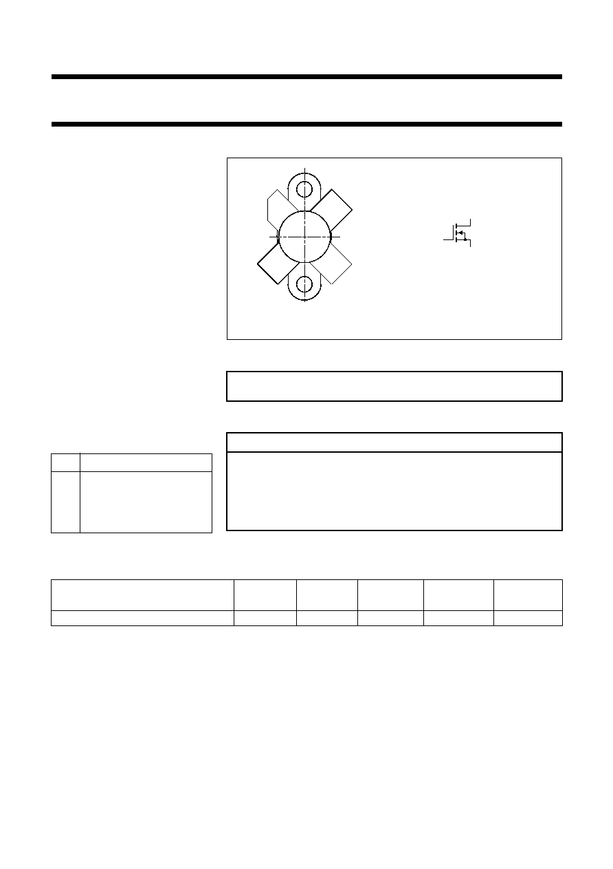
PINNING - SOT123
PIN
DESCRIPTION
1
drain
2
source
3
gate
4
source
PIN CONFIGURATION
CAUTION
The device is supplied in an antistatic package. The gate-source input must
be protected against static charge during transport and handling.
WARNING
Product and environmental safety - toxic materials
This product contains beryllium oxide. The product is entirely safe provided
that the BeO disc is not damaged. All persons who handle, use or dispose of
this product should be aware of its nature and of the necessary safety
precautions. After use, dispose of as chemical or special waste according to
the regulations applying at the location of the user. It must never be thrown
out with the general or domestic waste.
Fig.1 Simplified outline and symbol.
lfpage
1
2
3
4
MSB057
s
d
g
MBB072
QUICK REFERENCE DATA
RF performance at T
h
= 25
∞
C in a class-B test circuit.
MODE OF OPERATION
f
(MHz)
V
DS
(V)
P
L
(W)
G
p
(dB)
D
(%)
CW, class-B
175
28
30
>
13
>
50
September 1992
3
Philips Semiconductors
Product specification
VHF power MOS transistor
BLF245
LIMITING VALUES
In accordance with the Absolute Maximum System (IEC 134).
THERMAL RESISTANCE
SYMBOL
PARAMETER
CONDITIONS
MIN.
MAX.
UNIT
V
DS
drain-source voltage
V
GS
= 0
-
65
V
±
V
GS
gate-source voltage
V
DS
= 0
-
20
V
I
D
DC drain current
-
6
A
P
tot
total power dissipation
up to T
mb
= 25
∞
C
-
68
W
T
stg
storage temperature
-
65
150
∞
C
T
j
junction temperature
-
200
∞
C
SYMBOL
PARAMETER
CONDITIONS
THERMAL RESISTANCE
R
th j-mb
thermal resistance from
junction to mounting base
T
mb
= 25
∞
C; P
tot
= 68 W
2.6 K/W
R
th mb-h
thermal resistance from
mounting base to heatsink
T
mb
= 25
∞
C; P
tot
= 68 W
0.3 K/W
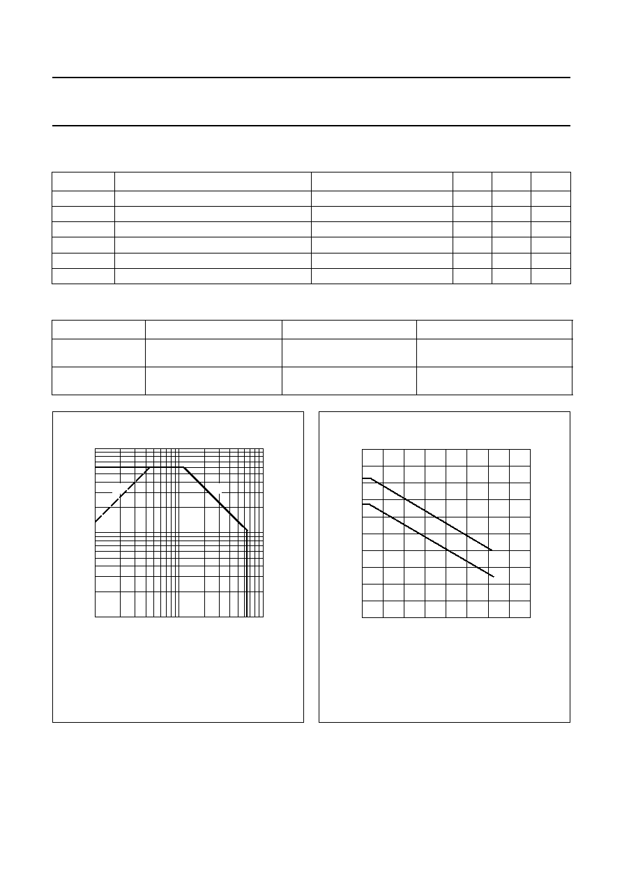
Fig.2 DC SOAR.
(1) Current is this area may be limited by R
DS(on)
.
(2) T
mb
= 25
∞
C.
handbook, halfpage
10
-
1
10
2
1
10
1
10
ID
(A)
VDS (V)
(1)
MRA921
(2)
Fig.3 Power/temperature derating curves.
(1) Continuous operation.
(2) Short-time operation during mismatch.
handbook, halfpage
0
40
80
160
100
80
40
20
0
60
120
MGP167
Ptot
(W)
Th (
∞
C)
(1)
(2)
September 1992
4
Philips Semiconductors
Product specification
VHF power MOS transistor
BLF245
CHARACTERISTICS
T
j
= 25
∞
C unless otherwise specified.
SYMBOL
PARAMETER
CONDITIONS
MIN.
TYP.
MAX. UNIT
V
(BR)DSS
drain-source breakdown voltage
V
GS
= 0; I
D
= 10 mA
65
-
-
V
I
DSS
drain-source leakage current
V
GS
= 0; V
DS
= 28 V
-
-
2
mA
I
GSS
gate-source leakage current
±
V
GS
= 20 V; V
DS
= 0
-
-
1
µ
A
V
GS(th)
gate-source threshold voltage
I
D
= 10 mA; V
DS
= 10 V
2
-
4.5
V
V
GS
gate-source voltage difference of
matched devices
I
D
= 10 mA; V
DS
= 10 V
-
-
100
mV
g
fs
forward transconductance
I
D
= 1.5 A; V
DS
= 10 V
1.2
1.9
-
S
R
DS(on)
drain-source on-state resistance
I
D
= 1.5 A; V
GS
= 10 V
-
0.4
0.75
I
DSX
on-state drain current
V
GS
= 10 V; V
DS
= 10 V
-
10
-
A
C
is
input capacitance
V
GS
= 0; V
DS
= 28 V; f = 1 MHz
-
125
-
pF
C
os
output capacitance
V
GS
= 0; V
DS
= 28 V; f = 1 MHz
-
75
-
pF
C
rs
feedback capacitance
V
GS
= 0; V
DS
= 28 V; f = 1 MHz
-
7
-
pF
F
noise figure (see Fig.14)
input and output power matched for:
I
D
= 1 A; V
DS
= 28 V; P
L
= 30 W;
R1 = 1 k
; T
h
= 25
∞
C; f = 175 MHz
-
2
-
dB
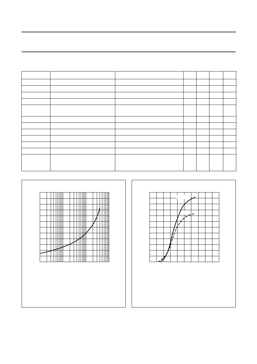
Fig.4
Temperature coefficient of gate-source
voltage as a function of drain current, typical
values.
V
DS
= 10 V; valid for T
j
= 25 to 125
∞
C.
handbook, halfpage
6
-
6
2
T.C.
(mV/K)
ID (mA)
-
2
4
0
-
4
MGP168
10
10
2
10
3
10
4
Fig.5
Drain current as a function of gate-source
voltage, typical values.
V
DS
= 10 V.
handbook, halfpage
0
20
12
0
4
8
10
MGP169
ID
(A)
VGS (V)
Tj = 25
∞
C
125
∞
C
September 1992
5
Philips Semiconductors
Product specification
VHF power MOS transistor
BLF245
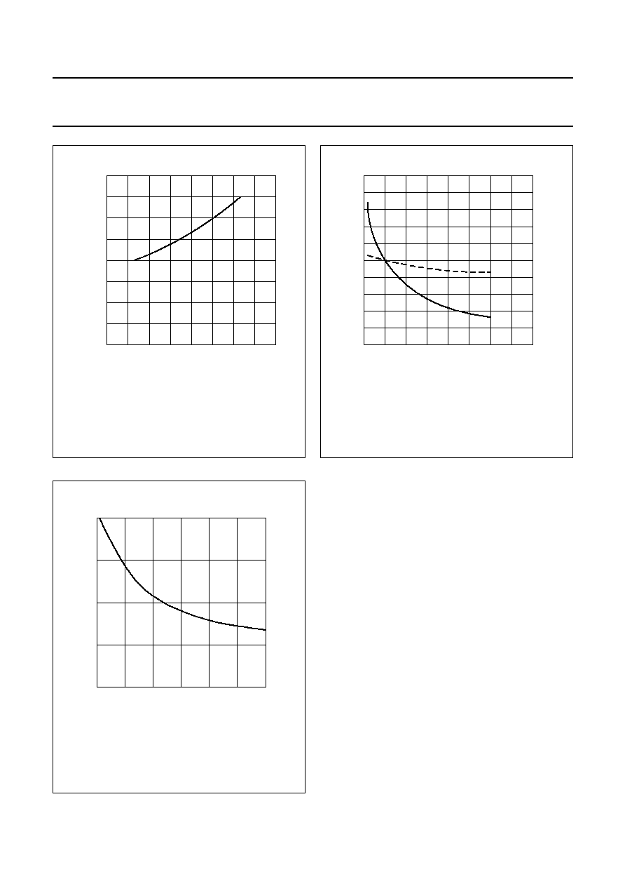
Fig.6
Drain-source on-state resistance as a
function of junction temperature, typical
values.
V
GS
= 10 V;
I
D
= 1.5 A.
handbook, halfpage
0
0.8
0.6
0.4
0
0.2
40
80
160
120
MGP170
RDS(on)
(
)
Tj (
∞
C)
Fig.7
Input and output capacitance as functions
of drain-source voltage, typical values.
V
GS
= 0; f = 1 MHz.
handbook, halfpage
0
10
20
40
240
40
200
30
160
120
80
MGP171
C
(pF)
VDS (V)
Cis
Cos
Fig.8
Feedback capacitance as a function of
drain-source voltage, typical values.
V
GS
= 0; f = 1 MHz.
handbook, halfpage
0
10
20
0
10
20
Crs
(pF)
VDS (V)
30
MRA920