BLF4G10-120; BLF4G10S-120 UHF power LDMOS transistor
1.
Product profile
1.1 General description
120 W LDMOS power transistor for base station applications at frequencies from
800 MHz to 1000 MHz.
[1]
ACPR
400
at 30 kHz resolution bandwidth
[2]
ACPR
600
at 30 kHz resolution bandwidth
1.2 Features
s
Typical GSM EDGE performance at frequency of 960 MHz, a supply voltage of 28 V
and an I
Dq
of 850 mA:
x
Load power = 48 W (AV)
x
Gain = 19 dB (typ)
x
Efficiency = 40 % (typ)
x
ACPR
400
=
-
61 dBc (typ)
x
ACPR
600
=
-
72 dBc (typ)
x
EVM
rms
= 1.5 % (typ)
s
Easy power control
s
Excellent ruggedness
s
High efficiency
s
Excellent thermal stability
s
Designed for broadband operation (800 MHz to 1000 MHz)
s
Internally matched for ease of use
BLF4G10-120; BLF4G10S-120
UHF power LDMOS transistor
Rev. 01 -- 10 January 2006
Product data sheet
Table 1:
Typical performance
RF performance at T
h
= 25
�
C in a common base class-AB test circuit.
Mode of
operation
f
(MHz)
V
DS
(V)
P
L
(W)
G
p
(dB)
(typ)
D
(%)
ACPR
400
(dBc)
(typ)
ACPR
600
(dBc)
(typ)
EVM
rms
(%)
IMD3
(dBc)
(typ)
CW
861 to 961 28
120
19
57
-
-
-
-
GSM EDGE 861 to 961 28
48 (AV)
19
40
-
61
[1]
-
72
[2]
1.5
-
2-tone
861 to 961 28
120 (PEP) 19
46
-
-
-
-
31
CAUTION
This device is sensitive to ElectroStatic Discharge (ESD). Therefore care should be taken
during transport and handling.
9397 750 14549
� Koninklijke Philips Electronics N.V. 2006. All rights reserved.
Product data sheet
Rev. 01 -- 10 January 2006
2 of 14
Philips Semiconductors
BLF4G10-120; BLF4G10S-120
UHF power LDMOS transistor
1.3 Applications
s
RF power amplifiers for GSM, GSM EDGE and CDMA base stations and multicarrier
applications in the 800 MHz to 1000 MHz frequency range.
2.
Pinning information
[1]
Connected to flange
3.
Ordering information
4.
Limiting values
Table 2:
Pinning
Pin
Description
Simplified outline
Symbol
BLF4G10-120 (SOT502A)
1
drain
2
gate
3
source
[1]
BLF4G10S-120 (SOT502B)
1
drain
2
gate
3
source
[1]
3
2
1
1
3
2
sym039
3
2
1
1
3
2
sym039
Table 3:
Ordering information
Type number
Package
Name
Description
Version
BLF4G10-120
-
flanged LDMOST ceramic package; 2 mounting
holes; 2 leads
SOT502A
BLF4G10S-120
-
earless flanged LDMOST ceramic package; 2 leads
SOT502B
Table 4:
Limiting values
In accordance with the Absolute Maximum Rating System (IEC 60134).
Symbol
Parameter
Conditions
Min
Max
Unit
V
DS
drain-source voltage
-
65
V
V
GS
gate-source voltage
-
0.5
+15
V
I
D
drain current
-
12
A
T
stg
storage temperature
-
65
+150
�
C
T
j
junction temperature
-
200
�
C

9397 750 14549
� Koninklijke Philips Electronics N.V. 2006. All rights reserved.
Product data sheet
Rev. 01 -- 10 January 2006
3 of 14
Philips Semiconductors
BLF4G10-120; BLF4G10S-120
UHF power LDMOS transistor
5.
Thermal characteristics
6.
Characteristics
7.
Application information
7.1 Ruggedness in class-AB operation
The BLF4G10-120 and BLF4G10S-120 are capable of withstanding a load mismatch
corresponding to VSWR = 10 : 1 through all phases under the following conditions:
V
DS
= 28 V; I
Dq
= 850 mA; P
L
= 120 W (CW); f = 960 MHz.
Table 5:
Thermal characteristics
Symbol
Parameter
Conditions
Min
Typ
Max
Unit
R
th(j-case)
thermal resistance from
junction to case
T
case
= 80
�
C
P
L
= 60 W
-
0.76
0.85
K/W
P
L
= 120 W
-
0.65
0.74
K/W
Table 6:
Characteristics
T
j
= 25
�
C; unless otherwise specified.
Symbol Parameter
Conditions
Min
Typ
Max
Unit
V
(BR)DSS
drain-source breakdown voltage V
GS
= 0 V; I
D
= 0.9 mA
65
-
-
V
V
GS(th)
gate-source threshold voltage
V
DS
= 10 V; I
D
= 180 mA
2.5
3.1
3.5
V
V
GSq
gate-source quiescent voltage
V
DS
= 28 V; I
D
= 900 mA
2.7
3.2
3.7
V
I
DSS
drain leakage current
V
GS
= 0 V; V
DS
= 28 V
-
-
3
�
A
I
DSX
drain cut-off current
V
GS
= V
GS(th)
+ 6 V;
V
DS
= 10 V
27
30
-
A
I
GSS
gate leakage current
V
GS
= 15 V; V
DS
= 0 V
-
-
300
nA
g
fs
forward transconductance
V
DS
= 10 V; I
D
= 10 A
-
9.0
-
S
R
DS(on)
drain-source on-state resistance V
GS
= V
GS(th)
+ 6 V;
I
D
= 6 A
-
0.09
-
C
rs
feedback capacitance
V
GS
= 0 V; V
DS
= 28 V;
f = 1 MHz
-
2.5
-
pF
Table 7:
Application information
Mode of operation: 2-tone (100 kHz tone spacing); f = 960 MHz.
V
DS
= 28 V; I
Dq
= 850 mA; T
case
= 25
�
C; unless otherwise specified.
Symbol
Parameter
Conditions
Min
Typ
Max
Unit
G
p
power gain
P
L(PEP)
= 120 W
18
19
-
dB
IRL
input return loss
P
L(PEP)
= 120 W
-
-
8
-
5
dB
D
drain efficiency
P
L(PEP)
= 120 W
44
46
-
%
IMD3
third order intermodulation
distortion
P
L(PEP)
= 120 W
-
-
31
-
27
dBc
9397 750 14549
� Koninklijke Philips Electronics N.V. 2006. All rights reserved.
Product data sheet
Rev. 01 -- 10 January 2006
4 of 14
Philips Semiconductors
BLF4G10-120; BLF4G10S-120
UHF power LDMOS transistor
V
DS
= 28 V; I
Dq
= 850 mA; T
case
= 25
�
C;
f = 960 MHz
V
DS
= 28 V; I
Dq
= 850 mA; T
case
= 25
�
C;
f = 960 MHz
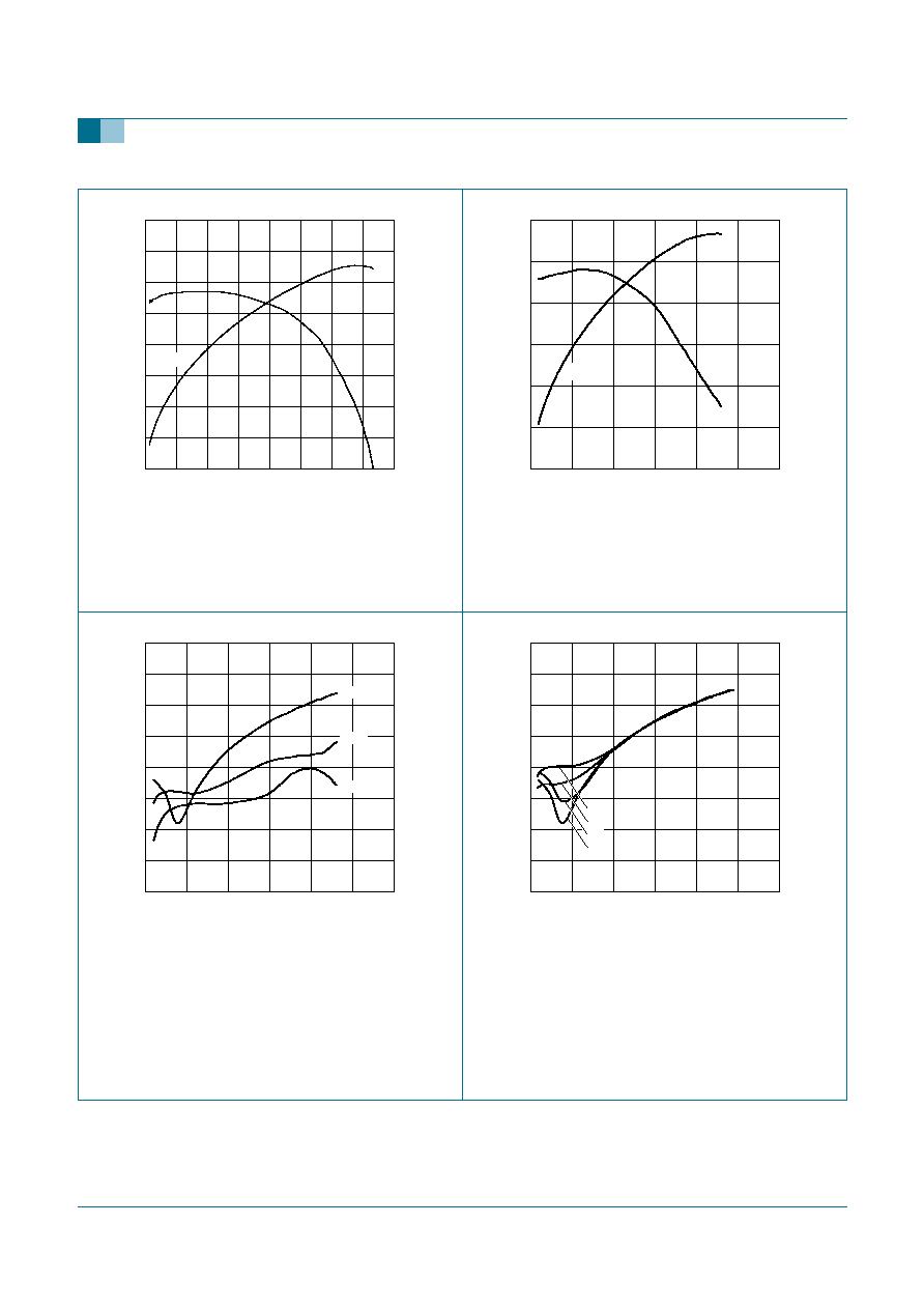
Fig 1.
One-tone CW power gain and drain efficiency
as functions of load power; typical values
Fig 2.
Two-tone CW power gain and drain efficiency
as functions of peak envelope load power;
typical values
V
DS
= 28 V; I
Dq
= 850 mA; T
case
= 25
�
C;
f = 960 MHz
V
DS
= 28 V; T
case
= 25
�
C; f = 960 MHz
(1) I
Dq
= 650 mA
(2) I
Dq
= 750 mA
(3) I
Dq
= 850 mA
(4) I
Dq
= 950 mA
Fig 3.
Intermodulation distortion as a function of peak
envelope load power; typical values
Fig 4.
Third order intermodulation distortion as a
function of peak envelope load power; typical
values
P
L
(W)
0
200
150
50
100
001aac400
18.5
40
17.5
19.5
20.5
G
p
(dB)
16.5
G
p
D
(%)
D
20
0
60
80
P
L(PEP)
(W)
0
300
200
100
001aac401
18
19
20
60
G
p
(dB)
17
40
20
0
G
p
D
(%)
D
001aac402
P
L(PEP)
(W)
0
300
200
100
-
40
-
60
-
20
0
IMD3
IMD5
IMD7
IMD
(dBc)
-
80
001aac403
P
L(PEP)
(W)
0
300
200
100
-
40
-
60
-
20
0
IMD3
(dBc)
-
80
2
1
4
3
9397 750 14549
� Koninklijke Philips Electronics N.V. 2006. All rights reserved.
Product data sheet
Rev. 01 -- 10 January 2006
5 of 14
Philips Semiconductors
BLF4G10-120; BLF4G10S-120
UHF power LDMOS transistor
V
DS
= 28 V; I
Dq
= 850 mA; T
case
= 25
�
C;
f = 960 MHz
V
DS
= 28 V; I
Dq
= 850 mA; T
case
= 25
�
C;
f = 960 MHz
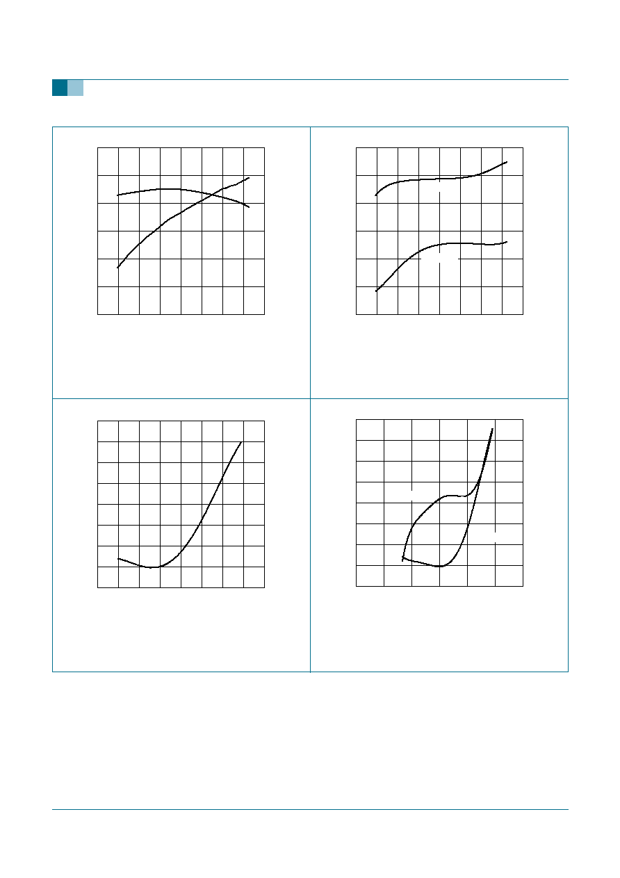
Fig 5.
GSM EDGE power gain and drain efficiency as
functions of average load power; typical values
Fig 6.
GSM EDGE ACPR at 400 kHz and at 600 kHz as
functions of average load power; typical values
V
DS
= 28 V; I
Dq
= 850 mA; T
case
= 25
�
C;
f = 960 MHz
V
DS
= 28 V; I
Dq
= 850 mA; T
case
= 25
�
C;
f = 960 MHz
Fig 7.
GSM EDGE rms EVM as a function of average
load power; typical values
Fig 8.
GSM EDGE ACPR at 400 kHz and rms EVM as
functions of drain efficiency; typical values
P
L(AV)
(W)
0
80
60
20
40
001aac404
18
19
40
20
G
p
(dB)
D
(%)
17
60
20
0
G
p
D
P
L(AV)
(W)
0
80
60
20
40
001aac405
-
75
-
65
-
55
ACPR
(dBc)
-
85
ACPR
400
ACPR
600
P
L(AV)
(W)
0
80
60
20
40
001aac406
2
1
3
4
EVM
rms
(%)
0
001aac407
D
(%)
0
60
40
20
-
61
-
63
-
59
3
-
57
ACPR
(dBc)
EVM
(%)
-
65
4
2
1
0
ACPR
400
EVM
rms
Document Outline