 | –≠–ª–µ–∫—Ç—Ä–æ–Ω–Ω—ã–π –∫–æ–º–ø–æ–Ω–µ–Ω—Ç: BU1706AB | –°–∫–∞—á–∞—Ç—å:  PDF PDF  ZIP ZIP |
Philips Semiconductors
Product specification
Silicon Diffused Power Transistor
BU1706AB
GENERAL DESCRIPTION
High-voltage, high-speed switching npn transistor in a plastic envelope suitable for surface mounting, intended for
use in high frequency electronic lighting ballast applications.
QUICK REFERENCE DATA
SYMBOL
PARAMETER
CONDITIONS
TYP.
MAX.
UNIT
V
CESM
Collector-emitter voltage peak value
V
BE
= 0 V
-
1750
V
V
CEO
Collector-emitter voltage (open base)
-
850
V
I
C
Collector current (DC)
-
5
A
I
CM
Collector current peak value
-
8
A
P
tot
Total power dissipation
T
mb
25 ∞C
-
100
W
V
CEsat
Collector-emitter saturation voltage
I
C
= 1.5 A; I
B
= 0.3 A
-
1.0
V
I
Csat
Collector saturation current
1.5
-
A
t
f
Fall time
I
CM
= 1.5 A; I
B(on)
= 0.3 A
0.25
0.6
µ
s
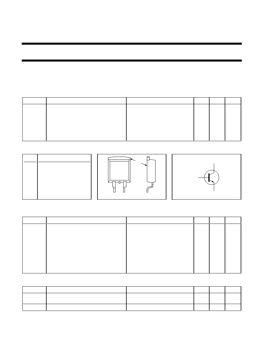
PINNING - SOT404
PIN CONFIGURATION
SYMBOL
PIN
DESCRIPTION
1
base
2
collector
3
emitter
mb
collector
LIMITING VALUES
Limiting values in accordance with the Absolute Maximum Rating System (IEC 134)
SYMBOL
PARAMETER
CONDITIONS
MIN.
MAX.
UNIT
V
CESM
Collector-emitter voltage peak value
V
BE
= 0 V
-
1750
V
V
CEO
Collector-emitter voltage (open base)
-
850
V
I
C
Collector current (DC)
-
5
A
I
CM
Collector current peak value
-
8
A
I
B
Base current (DC)
-
3
A
I
BM
Base current peak value
-
5
A
-I
B(AV)
Reverse base current
average over any 20ms period
-
100
mA
-I
BM
Reverse base current peak value
-
4
A
P
tot
Total power dissipation
T
mb
25 ∞C
-
100
W
T
stg
Storage temperature
-65
150
∞C
T
j
Junction temperature
-
150
∞C
THERMAL RESISTANCES
SYMBOL
PARAMETER
CONDITIONS
TYP.
MAX.
UNIT
R
th j-mb
Thermal resistance junction to mounting
-
1.25
K/W
base
R
th j-a
Thermal resistance junction to ambient
minimum footprint, FR4 board
55
-
K/W
1
3
mb
2
b
c
e
February 1998
1
Rev 1.000
Philips Semiconductors
Product specification
Silicon Diffused Power Transistor
BU1706AB
STATIC CHARACTERISTICS
T
mb
= 25 ∞C unless otherwise specified
SYMBOL
PARAMETER
CONDITIONS
MIN.
TYP.
MAX.
UNIT
I
CES
Collector cut-off current
1
V
BE
= 0 V; V
CE
= V
CESMmax
-
-
1.0
mA
I
CES
V
BE
= 0 V; V
CE
= 1500 V
-
-
20
µ
A
I
CES
V
BE
= 0 V; V
CE
= V
CESMmax
;
-
-
2.0
mA
T
j
= 125 ∞C
I
EBO
Emitter cut-off current
V
EB
= 12 V; I
C
= 0 A
-
-
1
mA
V
CEOsust
Collector-emitter sustaining voltage
I
B
= 0 A; I
C
= 100 mA;
750
-
-
V
L = 25 mH
V
CEsat
Collector-emitter saturation voltage
I
C
= 1.5 A; I
B
= 0.3 A
-
-
1.0
V
V
BEsat
Base-emitter saturation voltage
I
C
= 1.5 A; I
B
= 0.3 A
-
-
1.3
V
h
FE
DC current gain
I
C
= 5 mA; V
CE
= 10 V
8
-
-
h
FE
I
C
= 400 mA; V
CE
= 3 V
12
18
35
h
FE
I
C
= 1.5 A; V
CE
= 1 V
5
7
-
DYNAMIC CHARACTERISTICS
T
mb
= 25 ∞C unless otherwise specified
SYMBOL
PARAMETER
CONDITIONS
TYP.
MAX.
UNIT
Switching times (resistive load)
I
Con
= 1.5 A; I
Bon
= -I
Boff
= 0.3 A
t
on
Turn-on time
1.1
1.5
µ
s
t
s
Turn-off storage time
5
6.5
µ
s
t
f
Turn-off fall time
0.75
1.0
µ
s
Switching times (inductive load)
I
Con
= 1.5 A; I
Bon
= 0.3 A; L
B
= 1
µ
H;
-V
BB
= 5 V
t
s
Turn-off storage time
2.0
3.0
µ
s
t
f
Turn-off fall time
0.25
0.6
µ
s
Switching times (inductive load)
I
Con
= 1.5 A; I
Bon
= 0.3 A; L
B
= 1
µ
H;
-V
BB
= 5 V; T
j
= 100 ∞C
t
s
Turn-off storage time
2.2
3.3
µ
s
t
f
Turn-off fall time
0.2
0.7
µ
s
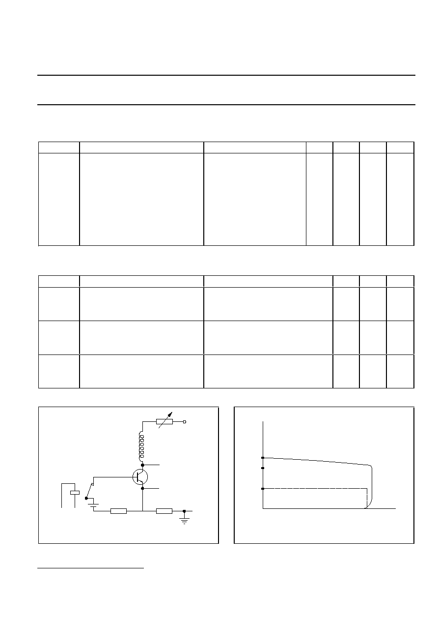
Fig.1. Test circuit for V
CEOsust
.
Fig.2. Oscilloscope display for V
CEOsust
.
+ 50v
100-200R
Horizontal
Vertical
Oscilloscope
1R
6V
30-60 Hz
300R
VCE / V
min
VCEOsust
IC / mA
100
200
250
0
1 Measured with half sine-wave voltage (curve tracer).
February 1998
2
Rev 1.000
Philips Semiconductors
Product specification
Silicon Diffused Power Transistor
BU1706AB
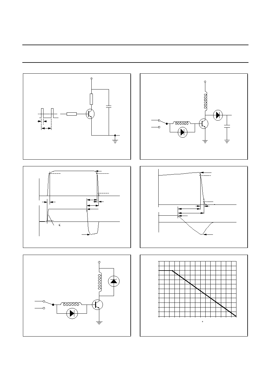
Fig.3. Test circuit resistive load. V
IM
= -6 to +8 V
V
CC
= 250 V; tp = 20
µ
s;
= tp / T = 0.01.
R
B
and R
L
calculated from I
Con
and I
Bon
requirements.
Fig.4. Switching times waveforms with resistive load.
Fig.5. Test circuit inductive load.
V
CC
= 300 V; -V
BE
= 5 V; L
B
= 1 uH
Fig.6. Test Circuit RBSOA.
V
CC
= 150 V; -V
BB
= 5 V; L
C
= 2 mH; V
CL
1500 V;
L
B
= 1
µ
H
Fig.7. Switching times waveforms with inductive load.
Fig.8. Normalised power dissipation.
PD% = 100
PD/PD
25 ∞C
= f (T
mb
)
tp
T
VCC
R
R
T.U.T.
0
VIM
B
L
LB
IBon
-VBB
LC
T.U.T.
VCC
VCL
IC
IB
10 %
10 %
90 %
90 %
ton
toff
ts
tf
IBon
-IBoff
ICon
tr
30ns
IC
IB
ICon
IBon
-IBoff
t
t
ts
tf
toff
10 %
90 %
LB
IBon
-VBB
LC
T.U.T.
VCC
0
20
40
60
80
100
120
140
Tmb / C
PD%
Normalised Power Derating
120
110
100
90
80
70
60
50
40
30
20
10
0
February 1998
3
Rev 1.000
Philips Semiconductors
Product specification
Silicon Diffused Power Transistor
BU1706AB
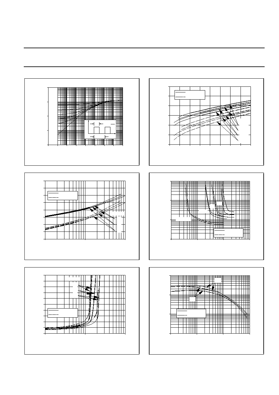
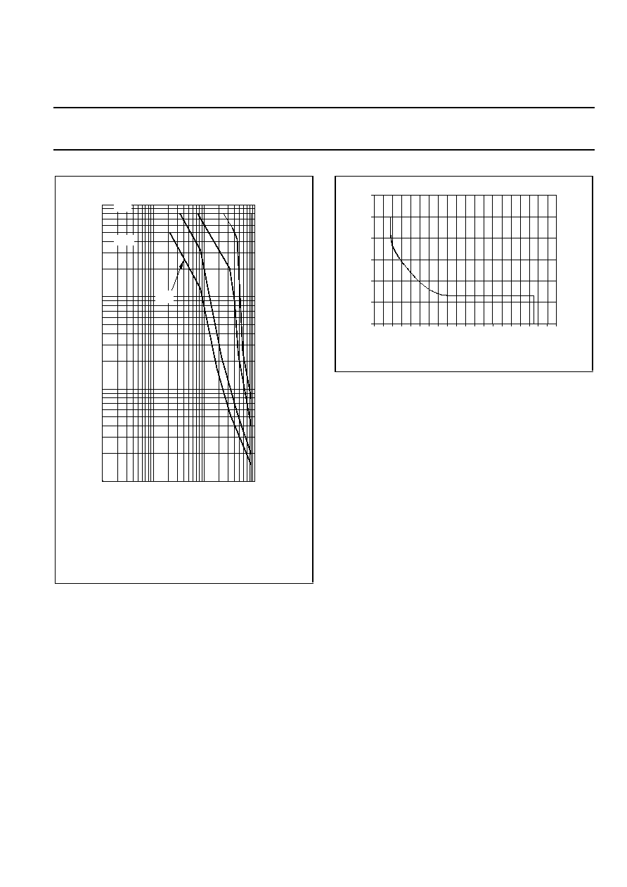
Fig.9. Transient thermal impedance.
Z
th j-mb
= f(t); parameter D = t
p
/T
Fig.10. Typical base-emitter saturation voltage.
V
BEsat
= f(I
C
); parameter I
C
/I
B
Fig.11. Typical collector-emitter saturation voltage.
V
CEsat
= f(I
C
); parameter I
C
/I
B
Fig.12. Typical base-emitter saturation voltage.
V
BEsat
= f(I
B
); parameter I
C
Fig.13. Typical collector-emitter saturation voltage.
V
CEsat
= f(I
B
); parameter I
C
Fig.14. Typical DC current gain.
h
FE
= f(I
C
); parameter V
CE
1E-07
1E-05
1E-03
1E-01
1E+01
t / s
Zth / (K/W)
1E+01
1E+00
1E-01
1E-02
1E-03
0
0.5
0.2
0.1
0.05
0.02
D=
BU1706A
D =
tp
T
T
P
t
D
t
p
0
1
2
3
4
IB / A
BU1706A
1.2
1.1
1
0.9
0.8
0.7
0.6
VBESAT / V
IC =
3 A
2 A
1.5 A
0.5 A
Tj = 25 C
Tj = 125 C
0.1
1
10
IC / A
VBESAT / V
BU1706A
1.2
1.1
1
0.9
0.8
0.7
0.6
0.5
0.4
IC/IB =
5
4
6
Tj = 25 C
Tj = 125 C
0.01
1
IB / A
VCESAT / V
BU1706A
10
1
0.1
0.01
0.1
10
IC = 0.5A
1.5 A
2A
3A
Tj = 25 C
Tj = 125 C
0.1
1
10
IC / A
VCESAT / V
BU1706A
1
0.9
0.8
0.7
0.6
0.5
0.4
0.3
0.2
0.1
0
IC/IB =
5
6
4
Tj = 25 C
Tj = 125 C
0.01
1
IC / A
BU1706A
100
10
1
0.1
0.1
10
h
FE
1 V
5 V
Tj = 25 C
Tj = 125 C
February 1998
4
Rev 1.000
Philips Semiconductors
Product specification
Silicon Diffused Power Transistor
BU1706AB
Fig.15. Forward bias safe operating area. T
mb
= 25 ∞C
I
Region of permissible DC operation.
II
Extension for repetitive pulse operation.
NB:
Mounted with heatsink compound and
30
±
5 newton force on the centre of the
envelope.
Fig.16. Reverse bias safe operating area. T
j
T
jmax
IC / A
VCE / V
0.01
0.1
1
10
1
10
100
1000
tp =
100 us
1 ms
10 ms
DC
CDC
I
CM
I
tot
P
6
5
4
3
2
1
0
0
400
800
1200
1600
2000
IC / A
BU1706A
VCE / V
February 1998
5
Rev 1.000