
Philips Semiconductors
Product specification
Silicon Diffused Power Transistor
BU2508DF
GENERAL DESCRIPTION
Enhanced performance, new generation, high-voltage, high-speed switching npn transistor with an integrated
damper diode in a plastic full-pack envelope intended for use in horizontal deflection circuits of colour television
receivers. Features exceptional tolerance to base drive and collector current load variations resulting in a very low
worst case dissipation.
QUICK REFERENCE DATA
SYMBOL
PARAMETER
CONDITIONS
TYP.
MAX.
UNIT
V
CESM
Collector-emitter voltage peak value
V
BE
= 0 V
-
1500
V
V
CEO
Collector-emitter voltage (open base)
-
700
V
I
C
Collector current (DC)
-
8
A
I
CM
Collector current peak value
-
15
A
P
tot
Total power dissipation
T
hs
25 �C
-
45
W
V
CEsat
Collector-emitter saturation voltage
I
C
= 4.5 A; I
B
= 1.12 A
-
1.0
V
I
Csat
Collector saturation current
4.5
-
A
V
F
Diode forward voltage
I
F
= 4.5 A
1.6
2.0
V
t
f
Fall time
I
Csat
= 4.5 A; I
B(end)
= 1.1 A
0.4
0.6
�
s
PINNING - SOT199
PIN CONFIGURATION
SYMBOL
PIN
DESCRIPTION
1
base
2
collector
3
emitter
case isolated
LIMITING VALUES
Limiting values in accordance with the Absolute Maximum Rating System (IEC 134)
SYMBOL
PARAMETER
CONDITIONS
MIN.
MAX.
UNIT
V
CESM
Collector-emitter voltage peak value
V
BE
= 0 V
-
1500
V
V
CEO
Collector-emitter voltage (open base)
-
700
V
I
C
Collector current (DC)
-
8
A
I
CM
Collector current peak value
-
15
A
I
B
Base current (DC)
-
4
A
I
BM
Base current peak value
-
6
A
-I
B(AV)
Reverse base current
average over any 20 ms period
-
100
mA
-I
BM
Reverse base current peak value
1
-
5
A
P
tot
Total power dissipation
T
hs
25 �C
-
45
W
T
stg
Storage temperature
-65
150
�C
T
j
Junction temperature
-
150
�C
1
2
3
case
b
c
e
Rbe
1 Turn-off current.
July 1998
1
Rev 1.600

Philips Semiconductors
Product specification
Silicon Diffused Power Transistor
BU2508DF
THERMAL RESISTANCES
SYMBOL
PARAMETER
CONDITIONS
TYP.
MAX.
UNIT
R
th j-hs
Junction to heatsink
without heatsink compound
-
3.7
K/W
R
th j-hs
Junction to heatsink
with heatsink compound
-
2.8
K/W
R
th j-a
Junction to ambient
in free air
35
-
K/W
ISOLATION LIMITING VALUE & CHARACTERISTIC
T
hs
= 25 �C unless otherwise specified
SYMBOL
PARAMETER
CONDITIONS
MIN.
TYP.
MAX.
UNIT
V
isol
Repetitive peak voltage from all
R.H.
65 % ; clean and dustfree
-
2500
V
three terminals to external
heatsink
C
isol
Capacitance from T2 to external f = 1 MHz
-
22
-
pF
heatsink
STATIC CHARACTERISTICS
T
hs
= 25 �C unless otherwise specified
SYMBOL
PARAMETER
CONDITIONS
MIN.
TYP.
MAX.
UNIT
I
CES
Collector cut-off current
2
V
BE
= 0 V; V
CE
= V
CESMmax
-
-
1.0
mA
I
CES
V
BE
= 0 V; V
CE
= V
CESMmax
;
-
-
2.0
mA
T
j
= 125 �C
I
EBO
Emitter cut-off current
V
EB
= 7.5 V; I
C
= 0 A
-
227
-
mA
BV
EBO
Emitter-base breakdown voltage
I
B
= 600 mA
7.5
13.5
-
V
R
be
Base-emitter resistance
V
EB
= 7.5 V
-
33
-
V
CEOsust
Collector-emitter sustaining voltage
I
B
= 0 A; I
C
= 100 mA;
700
-
-
V
L = 25 mH
V
CEsat
Collector-emitter saturation voltage
I
C
= 4.5 A; I
B
= 1.12 A
-
-
1.0
V
V
BEsat
Base-emitter saturation voltage
I
C
= 4.5 A; I
B
= 1.7 A
-
-
1.1
V
h
FE
DC current gain
I
C
= 1 A; V
CE
= 5 V
-
13
-
h
FE
I
C
= 4.5 A; V
CE
= 1 V
4
5.5
7.0
V
F
Diode forward voltage
I
F
= 4.5 A
-
1.6
2.0
V
DYNAMIC CHARACTERISTICS
T
hs
= 25 �C unless otherwise specified
SYMBOL
PARAMETER
CONDITIONS
TYP.
MAX.
UNIT
C
c
Collector capacitance
I
E
= 0 A; V
CB
= 10 V; f = 1 MHz
80
-
pF
Switching times (16 kHz line
I
Csat
= 4.5 A; I
B(end)
= 1.1 A; L
B
= 6
�
H;
deflection circuit)
-V
BB
= 4 V; (-dI
B
/dt = 0.6 A/
�
s)
t
s
Turn-off storage time
5.0
6.0
�
s
t
f
Turn-off fall time
0.4
0.6
�
s
Switching times (38 kHz line
I
Csat
= 4.0 A; I
B(end)
= 0.9 A; L
B
= 6
�
H;
deflectioin circuit)
-V
BB
= 4 V; (-dI
B
/dt = 0.6 A/
�
s)
t
s
Turn-off storage time
4.7
5.7
�
s
t
f
Turn-off fall time
0.25
0.35
�
s
2 Measured with half sine-wave voltage (curve tracer).
July 1998
2
Rev 1.600

Philips Semiconductors
Product specification
Silicon Diffused Power Transistor
BU2508DF
Fig.1. 16kHz Switching times waveforms.
Fig.2. Switching times definitions.
Fig.3. 16kHz Switching times test circuit.
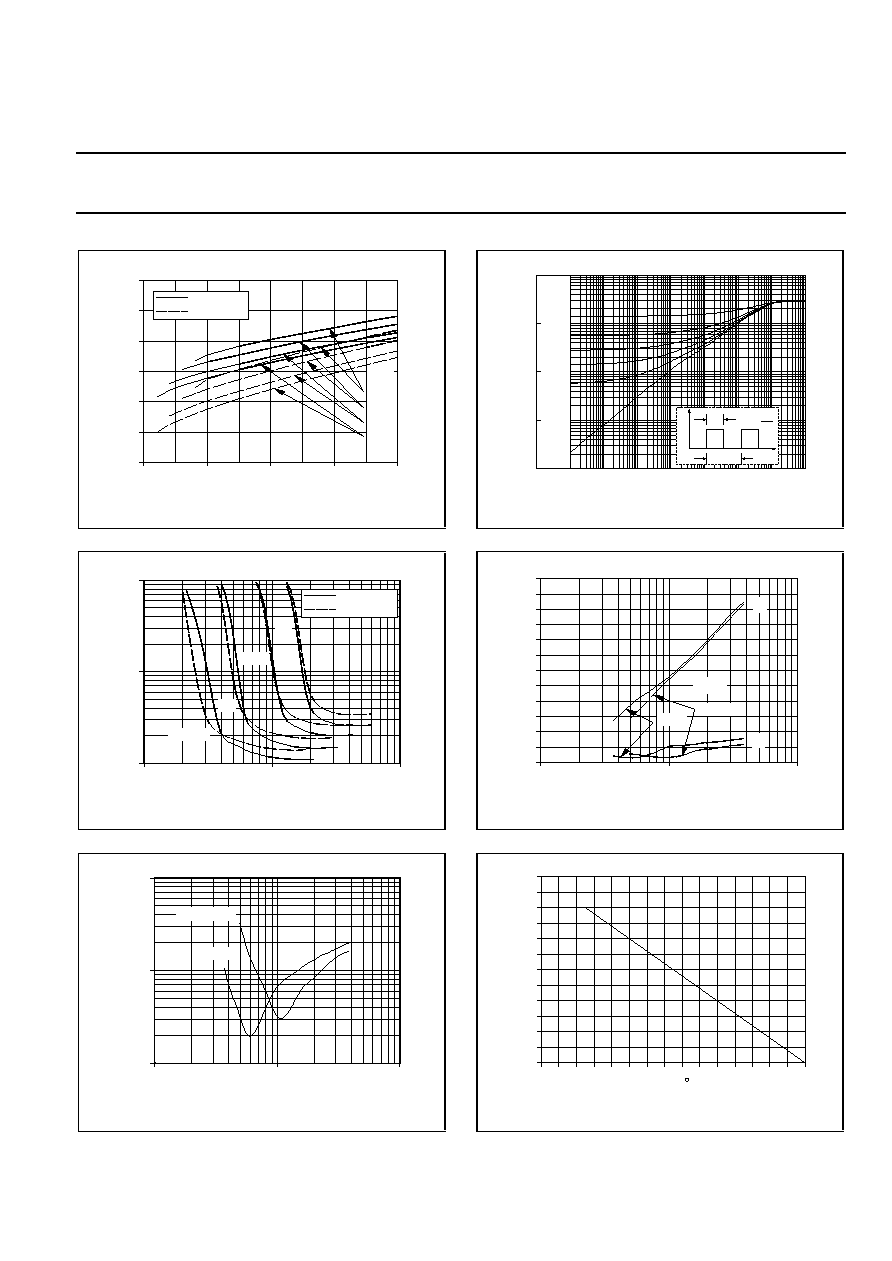
Fig.4. Typical DC current gain. h
FE
= f (I
C
)
parameter V
CE
Fig.5. Typical base-emitter saturation voltage.
V
BE
sat = f (I
C
); parameter I
C
/I
B
Fig.6. Typical collector-emitter saturation voltage.
V
CE
sat = f (I
C
); parameter I
C
/I
B
IC
IB
VCE
ICsat
IBend
64us
26us
20us
t
t
t
TRANSISTOR
DIODE
0.01
1
IC / A
BU2508DF
100
10
1
0.1
10
Tj = 25 C
Tj = 125 C
5V
h
FE
1V
ICsat
90 %
10 %
tf
ts
IBend
IC
IB
t
t
- IBM
0.1
1
10
IC / A
VBESAT / V
BU2508DF
1.2
1.1
1
0.9
0.8
0.7
0.6
0.5
0.4
Tj = 25 C
Tj = 125 C
IC/IB=
3
4
5
+ 150 v nominal
adjust for ICsat
1mH
12nF
D.U.T.
LB
IBend
-VBB
Rbe
0.1
1
10
IC / A
VCESAT / V
BU2508DF
1
0.9
0.8
0.7
0.6
0.5
0.4
0.3
0.2
0.1
0
Tj = 25 C
Tj = 125 C
IC/IB=
4
5
3
July 1998
3
Rev 1.600
Philips Semiconductors
Product specification
Silicon Diffused Power Transistor
BU2508DF
Fig.7. Typical base-emitter saturation voltage.
V
BE
sat = f (I
B
); parameter I
C
Fig.8. Typical collector-emitter saturation voltage.
V
CE
sat = f (I
B
); parameter I
C
Fig.9. Typical turn-off losses. T
j
= 85�C
Eoff = f (I
B
); parameter I
C
; f = 16 kHz
Fig.10. Transient thermal impedance.
Z
th j-hs
= f(t); parameter D = t
p
/T
Fig.11. Typical collector storage and fall time.
ts = f (I
B
); tf = f (I
B
); parameter I
C
; T
j
= 85�C; f = 16 kHz
Fig.12. Normalised power dissipation.
PD% = 100
P
D
/P
D 25�C
= f (T
hs
)
0
1
2
3
4
IB / A
VBESAT / V
BU2508DF
1.2
1.1
1
0.9
0.8
0.7
0.6
Tj = 25 C
Tj = 125 C
IC=
6A
4.5A
3A
2A
0.001
0.01
0.1
1
10
0
0.2
0.1
0.05
0.02
0.5
BU2508AX
tp / sec
Zth K/W
1.0E-06
1E-04
1E-02
1E+00
D =
tp
tp
T
T
P
t
D
0.1
1
10
IB / A
VCESAT / V
BU2508DF
10
1
0.1
Tj = 25 C
Tj = 125 C
Tj = 25 C
Tj = 125 C
IC=2A
3A
4.5A
6A
0.1
1
10
IB / A
ts, tf / us
BU2508DF
12
11
10
9
8
7
6
5
4
3
2
1
0
IC =
4.5A
3.5A
ts
tf
0.1
1
10
IB / A
Eoff / uJ
BU2508DF
1000
100
10
IC = 4.5A
3.5A
0
20
40
60
80
100
120
140
Ths / C
PD%
Normalised Power Derating
120
110
100
90
80
70
60
50
40
30
20
10
0
with heatsink compound
July 1998
4
Rev 1.600

Philips Semiconductors
Product specification
Silicon Diffused Power Transistor
BU2508DF
Fig.13. Forward bias safe operating area. T
hs
= 25�C
I
Region of permissible DC operation.
II
Extension for repetitive pulse operation.
NB:
Mounted with heatsink compound and
30
�
5 newton force on the centre of
the envelope.
Fig.14. Forward bias safe operating area. T
hs
= 25�C
I
Region of permissible DC operation.
II
Extension for repetitive pulse operation.
NB:
Mounted without heatsink compound and
30
�
5 newton force on the centre of
the envelope.
1
10
100
1000
100
10
1
0.1
0.01
tp =
10 us
100 us
1 ms
10 ms
DC
IC / A
VCE / V
ICM max
IC max
= 0.01
II
I
Ptot max
1
10
100
1000
100
10
1
0.1
0.01
tp =
10 us
100 us
1 ms
10 ms
DC
IC / A
VCE / V
ICM max
IC max
= 0.01
II
I
Ptot max
July 1998
5
Rev 1.600