 | ÐлекÑÑоннÑй компоненÑ: BYM359X | СкаÑаÑÑ:  PDF PDF  ZIP ZIP |
Äîêóìåíòàöèÿ è îïèñàíèÿ www.docs.chipfind.ru
Philips Semiconductors
Product specification
Dual diode
BYM359X
fast, high-voltage
FEATURES
SYMBOL
QUICK REFERENCE DATA
· Low forward volt drop
DAMPER
MODULATOR
· Fast switching
· Soft recovery characteristic
V
R
=1500 V
V
R
=800 V
· High thermal cycling
performance
V
F
1.3 V
V
F
1.45 V
· Isolated mounting tab
I
F(RMS)
=15.7 A
I
F(RMS)
= 11 A
I
FSM
60 A
I
FSM
60 A
t
rr
300 ns
t
rr
145 ns
GENERAL DESCRIPTION
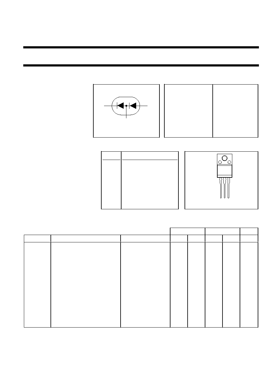
PINNING
SOT186A
Combined damper and modulator
PIN
DESCRIPTION
diodes
in
an
isolated
plastic
envelope for horizontal deflection in
1
damper cathode
colour TV and PC monitors.
The BYM359X contains diodes
2
common anode/cathode
with performance characteristics
designed specifically for
3
modulator anode.
applications from 16kHz to 56kHz
The BYM359X series is supplied in
the conventional leaded SOT186A
package.
LIMITING VALUES
T
j
= 25 °C unless otherwise stated
DAMPER
MODULATOR
SYMBOL
PARAMETER
CONDITIONS
MIN
MAX
MIN
MAX
UNIT
V
RSM
Peak non-repetitive reverse
-
1500
-
800
V
voltage.
V
RRM
Peak repetitive reverse voltage
-
1500
-
600
V
V
RWM
Crest working reverse voltage
-
1300
-
600
V
I
F(AV)
Average forward current
sinusoidal;a=1.57
-
10
-
8
A
I
F(RMS)
RMS forward current
-
15.7
-
11.0
A
I
FRM
Peak repetitive forward current
t=25
µ
s
= 0.5
-
20
-
16.0
A
T
hs
83 °C
I
FSM
Peak non-repetitive forward
t = 10ms
-
60
-
60
A
current
t = 8.3 ms
-
66
-
66
A
sinusoidal;
with reapplied
V
RWM(MAX)
T
stg
Storage temperature
-40
150
-40
150
°C
T
J
Operating junction temperature
-
150
-
150
°C
1
3
2
damper
modulator
1 2 3
case
December 1999
1
Rev 1.200

Philips Semiconductors
Product specification
Dual diode
BYM359X
fast, high-voltage
ISOLATION LIMITING VALUE & CHARACTERISTIC
T
hs
= 25 °C unless otherwise specified
SYMBOL
PARAMETER
CONDITIONS
MIN.
TYP.
MAX.
UNIT
V
isol
R.M.S. isolation voltage from all
f = 50-60 Hz; sinusoidal
-
-
2500
V
three terminals to external
waveform;
heatsink
R.H.
65% ; clean and dustfree
C
isol
Capacitance from T2 to external f = 1 MHz
-
10
-
pF
heatsink
THERMAL RESISTANCES
DAMPER
MODULATOR
SYMBOL
PARAMETER
CONDITIONS
TYP.
MAX.
TYP.
MAX.
UNIT
R
th j-hs
Thermal resistance junction to
with heatsink
-
4.8
-
4.8
K/W
heatsink
compound
R
th j-a
Thermal resistance junction to
in free air.
55
-
-
55
K/W
ambient
STATIC CHARACTERISTICS
T
j
= 25 °C unless otherwise stated
DAMPER
MODULATOR
SYMBOL
PARAMETER
CONDITIONS
TYP.
MAX.
TYP.
MAX.
UNIT
V
F
Forward voltage
I
F
= 6.5 A
1.1
1.45
1.15
1.55
V
I
F
= 6.5 A; T
j
= 125°C
1.05
1.3
1.1
1.45
V
I
R
Reverse current
V
R
= V
RWM
10
250
10
100
µ
A
V
R
= V
RWM
50
500
100
600
µ
A
T
j
= 100 °C
DYNAMIC CHARACTERISTICS
T
j
= 25 °C unless otherwise stated
DAMPER
MODULATOR
SYMBOL
PARAMETER
CONDITIONS
TYP.
MAX.
TYP.
MAX.
UNIT
t
rr
Reverse recovery time
I
F
= 1 A; V
R
30 V;
200
300
125
145
ns
-dI
F
/dt = 50 A/
µ
s
Q
s
Reverse recovery charge
2 A,30 V,20 A/
µ
s
1.2
2.0
0.5
0.7
µ
C
V
fr
Peak forward recovery voltage
I
F
= 6.5 A;
27
-
18.0
-
V
dI
F
/dt = 50 A/
µ
s
December 1999
2
Rev 1.200
Philips Semiconductors
Product specification
Dual diode
BYM359X
fast, high-voltage
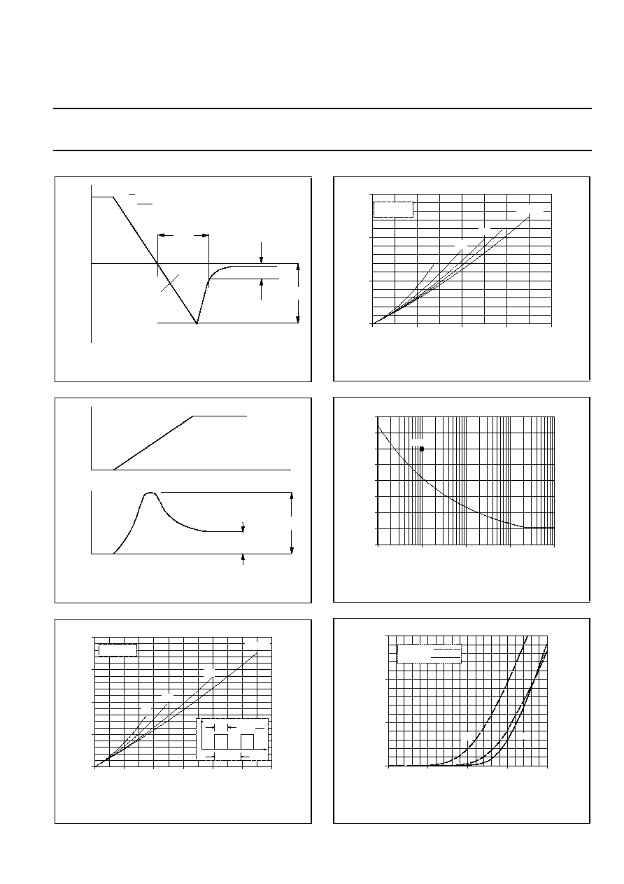
Fig.1. Definition of t
rr
, Q
s
and I
rrm
Fig.2. Definition of V
fr
Fig.3. Modulator maximum forward dissipation,
P
F
= f(I
F(AV)
); square wave current waveform;
parameter D = duty cycle = t
p
/T.
Fig.4. Modulator maximum forward dissipation,
P
F
= f(I
F(AV)
); sinusoidal current waveform; parameter
a = form factor = I
F(RMS)
/I
F(AV)
.
Fig.5. Modulator maximum non-repetitive rms forward
current. I
F
= f(t
p
); sinusoidal current waveform;
T
j
= 150°C prior to surge with reapplied V
RWM
.
Fig.6. Modulator typical and maximum forward
characteristic; I
F
= f(V
F
); parameter T
j
0
2
4
6
8
BY329
IF(AV) / A
PF / W
15
10
5
0
4
2.8
2.2
1.9
a = 1.57
Ths(max) / C
150
78
102
126
Vo = 1.25 V
Rs = 0.03 Ohms
100%
time
dI
dt
F
I
R
I
F
I
rrm
trr
25%
Qs
1ms
10ms
0.1s
1s
10s
tp / s
IFS(RMS) / A
BY229
80
70
60
50
40
30
20
10
0
IFSM
time
time
V F
V
fr
V F
I
F
0
1
BY229F
VF / V
IF / A
30
20
10
0
2
0.5
1.5
max
typ
Tj = 150 C
Tj = 25 C
0
2
4
6
8
10
12
BY329
IF(AV) / A
PF / W
20
15
10
5
0
Ths(max) / C
150
54
78
102
126
0.5
0.2
0.1
D = 1.0
D =
t
p
t
p
T
T
I
t
Vo = 1.25 V
Rs = 0.03 Ohms
December 1999
3
Rev 1.200
Philips Semiconductors
Product specification
Dual diode
BYM359X
fast, high-voltage
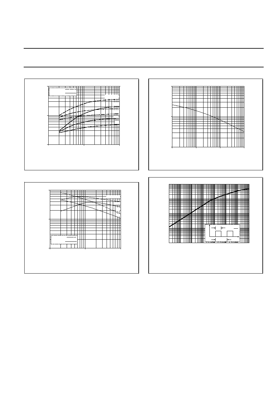
Fig.7. Modulator maximum Q
s
at T
j
= 25°C and 150°C
Fig.8. Modulator maximum t
rr
measured to 25% of I
rrm
;
T
j
= 25°C and 150°C
Fig.9. Modulator typical junction capacitance C
d
at
f = 1 MHz
;
T
j
= 25°C
Fig.10. Modulator transient thermal impedance
Z
th
= f(t
p
)
1
100
BY329
-dIF/dt (A/us)
Qs / uC
10
1
0.1
10
2 A
IF = 10 A
10 A
1 A
1 A
2 A
Tj = 150 C
Tj = 25 C
1
100
100
10
1
10
1000
BY329
Cd / pF
VR / V
1us
10us
100us
1ms
10ms
100ms
1s
10s
0.001
0.01
0.1
1
10
BY229F
pulse width, tp (s)
Transient thermal impedance, Zth j-hs (K/W)
D =
t
p
t
p
T
T
P
t
D
1
10
100
BY329
-dIF/dt (A/us)
trr / ns
1000
100
10
1 A
IF = 10 A
Tj = 150 C
Tj = 25 C
10A
1A
December 1999
4
Rev 1.200
Philips Semiconductors
Product specification
Dual diode
BYM359X
fast, high-voltage
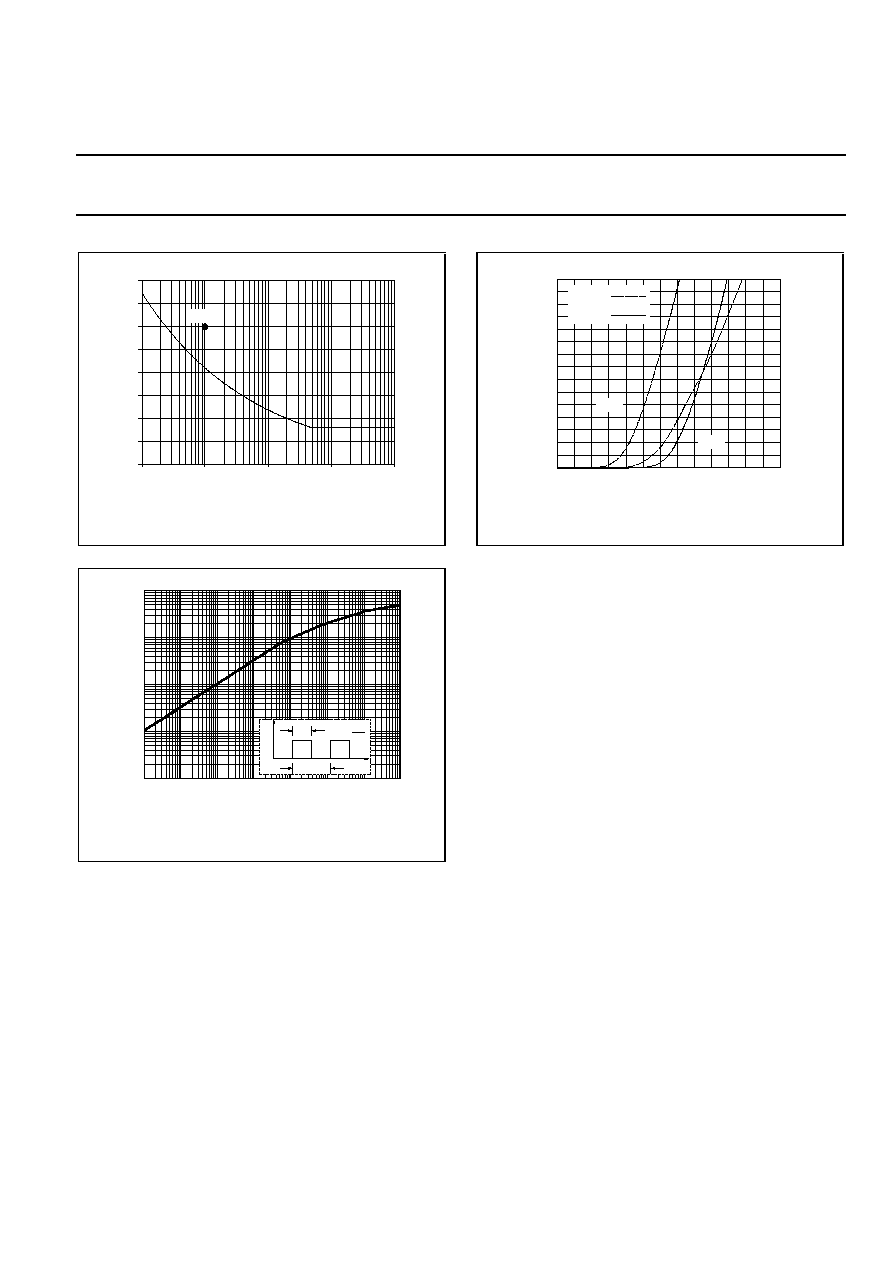
Fig.11. Damper maximum non-repetitive rms forward
current. I
F
= f(t
p
); sinusoidal current waveform;
T
j
= 150°C prior to surge with reapplied V
RWM
.
Fig.12. Damper transient thermal impedance
Z
th
= f(t
p
)
Fig.13. Damper forward characteristic I
F
= f(V
F
);
parameter T
j
1ms
10ms
0.1s
1s
10s
tp / s
IFS(RMS) / A
BY359
80
70
60
50
40
30
20
10
0
IFSM
0
30
20
10
0
1.0
2.0
IF / A
VF / V
max
typ
Tj=150C
Tj=25C
BY359
1us
10us
100us
1ms
10ms
100ms
1s
10s
0.001
0.01
0.1
1
10
BY359F
pulse width, tp (s)
Transient thermal impedance, Zth j-hs (K/W)
D =
t
p
t
p
T
T
P
t
D
December 1999
5
Rev 1.200
Philips Semiconductors
Product specification
Dual diode
BYM359X
fast, high-voltage
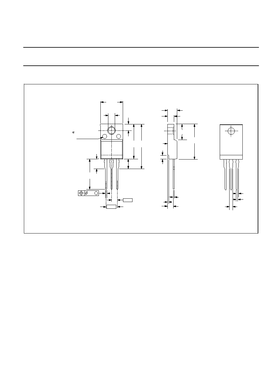
MECHANICAL DATA
Dimensions in mm
Net Mass: 2 g
Fig.14. SOT186A; The seating plane is electrically isolated from all terminals.
Notes
1. Refer to mounting instructions for F-pack envelopes.
2. Epoxy meets UL94 V0 at 1/8".
10.3
max
3.2
3.0
4.6
max
2.9 max
2.8
seating
plane
6.4
15.8
max
0.6
2.5
2.54
5.08
1
2
3
3 max.
not tinned
3
0.5
2.5
0.9
0.7
M
0.4
15.8
max.
19
max.
13.5
min.
Recesses (2x)
2.5
0.8 max. depth
1.0 (2x)
1.3
December 1999
6
Rev 1.200

Philips Semiconductors
Product specification
Dual diode
BYM359X
fast, high-voltage
DEFINITIONS
Data sheet status
Objective specification
This data sheet contains target or goal specifications for product development.
Preliminary specification This data sheet contains preliminary data; supplementary data may be published later.
Product specification
This data sheet contains final product specifications.
Limiting values
Limiting values are given in accordance with the Absolute Maximum Rating System (IEC 134). Stress above one
or more of the limiting values may cause permanent damage to the device. These are stress ratings only and
operation of the device at these or at any other conditions above those given in the Characteristics sections of
this specification is not implied. Exposure to limiting values for extended periods may affect device reliability.
Application information
Where application information is given, it is advisory and does not form part of the specification.
Philips Electronics N.V. 1999
All rights are reserved. Reproduction in whole or in part is prohibited without the prior written consent of the
copyright owner.
The information presented in this document does not form part of any quotation or contract, it is believed to be
accurate and reliable and may be changed without notice. No liability will be accepted by the publisher for any
consequence of its use. Publication thereof does not convey nor imply any license under patent or other
industrial or intellectual property rights.
LIFE SUPPORT APPLICATIONS
These products are not designed for use in life support appliances, devices or systems where malfunction of these
products can be reasonably expected to result in personal injury. Philips customers using or selling these products
for use in such applications do so at their own risk and agree to fully indemnify Philips for any damages resulting
from such improper use or sale.
December 1999
7
Rev 1.200