 | ÐлекÑÑоннÑй компоненÑ: BZA9xxA | СкаÑаÑÑ:  PDF PDF  ZIP ZIP |
Äîêóìåíòàöèÿ è îïèñàíèÿ www.docs.chipfind.ru
DATA SHEET
Product specification
2001 Sep 03
DISCRETE SEMICONDUCTORS
BZA900A-series
Quadruple ESD transient voltage
suppressor
M3D743
2001 Sep 03
2
Philips Semiconductors
Product specification
Quadruple ESD transient voltage suppressor
BZA900A-series
FEATURES
·
ESD rating >8 kV, according to IEC61000-4-2
·
SOT665 surface mount package
·
Common anode configuration.
APPLICATIONS
·
Computers and peripherals
·
Audio and video equipment
·
Communication systems
DESCRIPTION
Monolithic transient voltage suppressor diode in a five lead
SOT665 package for 4-bit wide ESD transient
suppression.
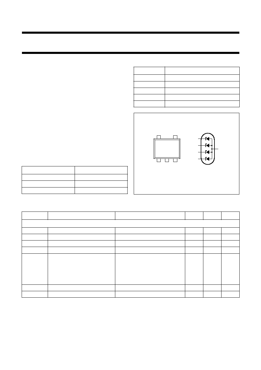
MARKING
PINNING
TYPE NUMBER
MARKING CODE
BZA956A
Z1
BZA962A
Z2
BZA968A
Z3
PIN
DESCRIPTION
1
cathode 1
2
common anode
3
cathode 2
4
cathode 3
5
cathode 4
handbook, halfpage
MGW315
1
5
4
3
2
1
2
3
4
5
Fig.1 Simplified outline (SOT665) and symbol.
LIMITING VALUES
In accordance with the Absolute Maximum Rating System (IEC 60134).
Notes
1. DC working current limited by P
tot(max)
.
2. Device mounted on standard printed-circuit board.
SYMBOL
PARAMETER
CONDITIONS
MIN.
MAX.
UNIT
Per diode
I
Z
working current
T
amb
= 25
°
C
-
note 1
mA
I
F
continuous forward current
T
amb
= 25
°
C
-
200
mA
I
FSM
non-repetitive peak forward current t
p
= 1 ms; square pulse
-
4
A
P
tot
total power dissipation
T
amb
= 25
°
C; note 2; see Fig.5
-
335
mW
P
ZSM
non repetitive peak reverse power
dissipation:
square pulse; t
p
= 1 ms; see Fig.3
BZA956A
-
16
W
BZA962A
-
15
W
BZA968A
-
14
W
T
stg
storage temperature
-
65
+150
°
C
T
j
junction temperature
-
150
°
C

2001 Sep 03
3
Philips Semiconductors
Product specification
Quadruple ESD transient voltage suppressor
BZA900A-series
THERMAL CHARACTERISTICS
Note
1. Solder point of common anode (pin 2).
ELECTRICAL CHARACTERISTICS
T
j
= 25
°
C unless otherwise specified.
Table 1
Per type; BZ956A to BZA968A
T
j
= 25
°
C unless otherwise specified.
SYMBOL
PARAMETER
CONDITIONS
VALUE
UNIT
R
th j-a
thermal resistance from junction to ambient
all diodes loaded
370
K/W
R
th j-s
thermal resistance from junction to solder
point; note 1
one diode loaded
135
K/W
all diodes loaded
125
K/W
SYMBOL
PARAMETER
CONDITIONS
MAX.
UNIT
V
F
forward voltage
I
F
= 200 mA
1.3
V
I
R
reverse current
BZA956A
V
R
= 3 V
1000
nA
BZA962A
V
R
= 4 V
500
nA
BZA968A
V
R
= 4.3 V
100
nA
TYPE
WORKING VOLTAGE
V
Z
(V)
at I
Z
= 1 mA
DIFFERENTIAL
RESISTANCE
r
dif
(
)
at I
Z
= 1 mA
TEMP.
COEFF.
S
Z
(mV/K) at
I
Z
= 1 mA
DIODE CAP.
C
d
(pF)
at f = 1 MHz;
V
R
= 0
NON-REPETITIVE
PEAK REVERSE
CURRENT
I
ZSM
(A) at t
p
= 1 ms;
T
amb
= 25
°
C
MIN.
TYP.
MAX.
MAX.
TYP.
MAX.
MAX.
BZA956A
5.32
5.6
5.88
400
0.3
125
2.2
BZA962A
5.89
6.2
6.51
300
1.6
105
2.1
BZA968A
6.46
6.8
7.14
200
2.2
90
2.0
2001 Sep 03
4
Philips Semiconductors
Product specification
Quadruple ESD transient voltage suppressor
BZA900A-series
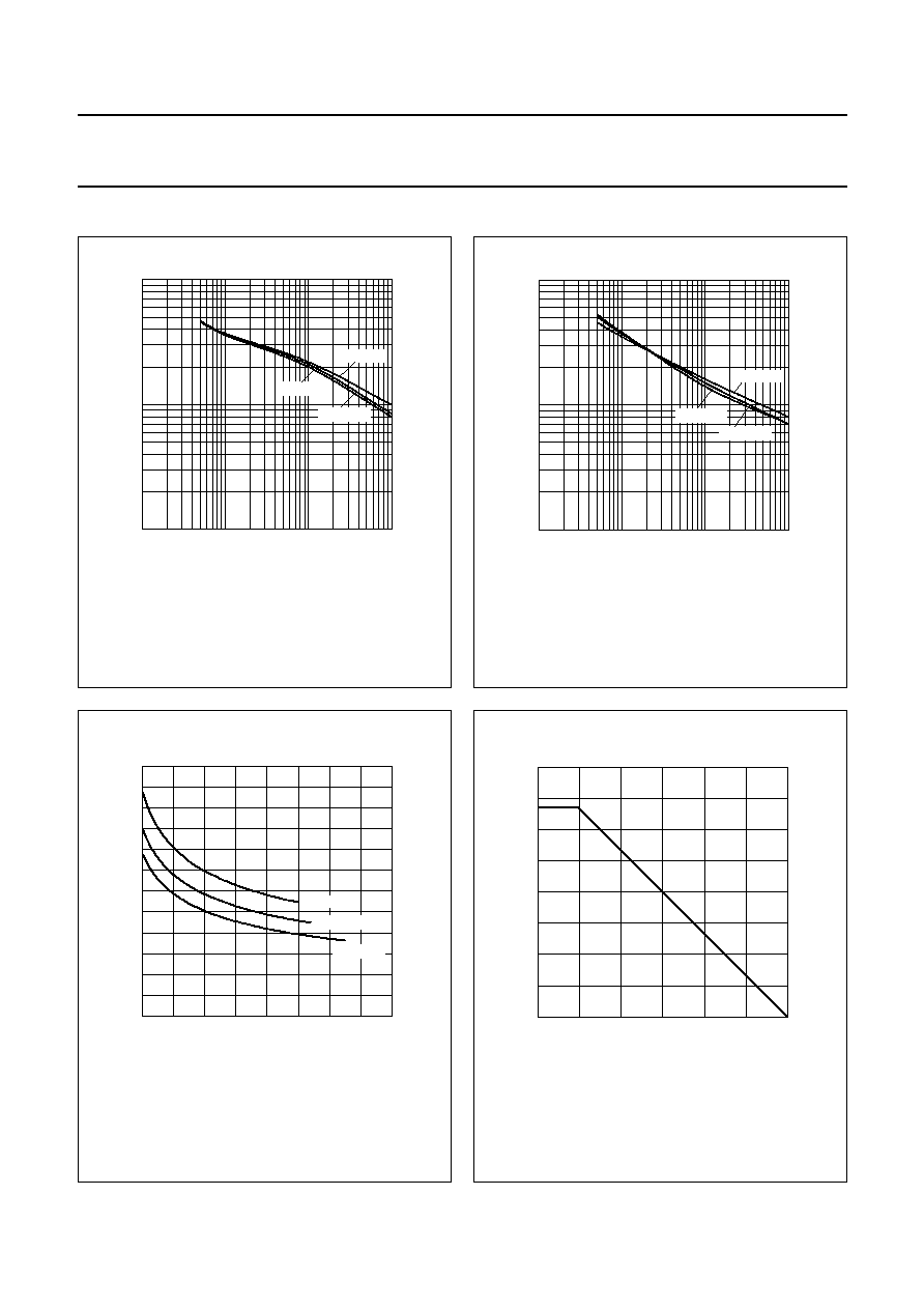
GRAPHICAL DATA
handbook, halfpage
10
1
MGW318
10
-
2
10
-
1
1
10
tp (ms)
IZSM
(A)
BZA956A
BZA968A
10
-
1
BZA962A
Fig.2
Maximum non-repetitive peak reverse
current as a function of pulse time.
handbook, halfpage
10
2
10
1
MGW319
10
-
2
10
-
1
1
10
tp (ms)
PZSM
(W)
BZA956A
BZA968A
BZA962A
Fig.3
Maximum non-repetitive peak reverse
power dissipation as a function of pulse
duration (square pulse).
P
ZSM
= V
ZSM
×
I
ZSM
.
V
ZSM
is the non-repetitive peak reverse voltage at I
ZSM
.
handbook, halfpage
0
2
6
8
120
0
MGW320
4
80
40
VR (V)
Cd
(pF)
BZA956A
BZA968A
BZA962A
Fig.4
Diode capacitance as a function of reverse
voltage; typical values.
T
j
= 25
°
C; f = 1 MHz.
handbook, halfpage
0
50
100
150
400
300
100
0
200
MGT586
Tamb (
°
C)
Ptot
(mW)
Fig.5 Power derating curve.
2001 Sep 03
5
Philips Semiconductors
Product specification
Quadruple ESD transient voltage suppressor
BZA900A-series
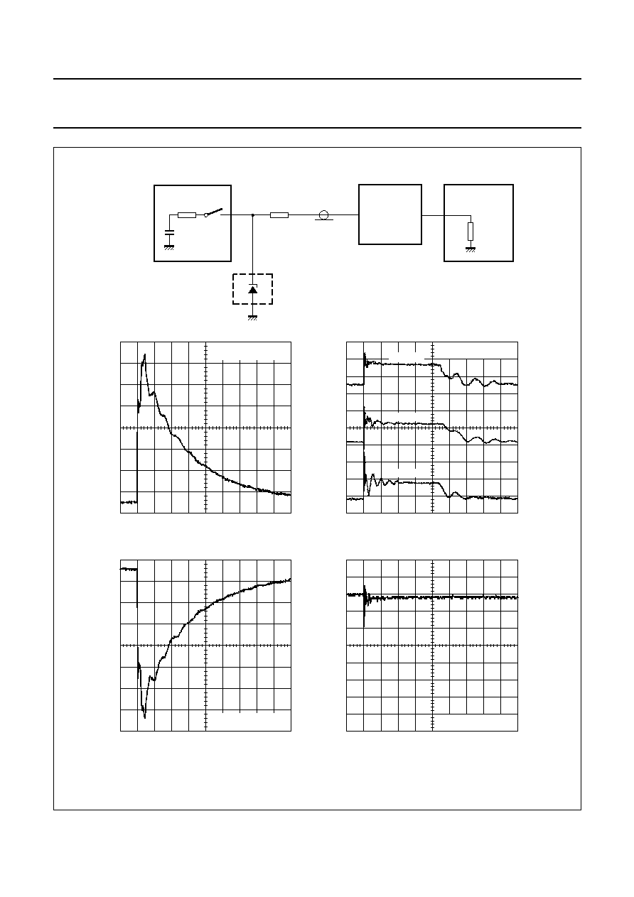
handbook, full pagewidth
MGW321
450
50
Note 1: attenuator is only used for open
socket high voltage measurements
IEC 61000-4-2 network
CZ = 150 pF; RZ = 330
1/4 BZA900A
RG 223/U
50
coax
RZ
CZ
ESD TESTER
DIGITIZING
OSCILLOSCOPE
10
×
ATTENUATOR
note 1
GND
GND
GND
unclamped
+
1 kV ESD voltage waveform
(IEC 61000-4-2 network)
clamped
+
1 kV ESD voltage waveform
(IEC 61000-4-2 network)
vertical scale = 100 V/div
horizontal scale = 50 ns/div
unclamped
-
1 kV ESD voltage waveform
(IEC 61000-4-2 network)
clamped
-
1 kV ESD voltage waveform
(IEC 61000-4-2 network)
vertical scale = 100 V/div
horizontal scale = 50 ns/div
vertical scale = 5 V/div
horizontal scale = 50 ns/div
vertical scale = 5 V/div
horizontal scale = 50 ns/div
BZA956A
BZA962A
BZA968A
Fig.6 ESD clamping test set-up and waveforms.
2001 Sep 03
6
Philips Semiconductors
Product specification
Quadruple ESD transient voltage suppressor
BZA900A-series
APPLICATION INFORMATION
Typical common anode application
A quadruple transient suppressor in a SOT665 package makes it possible to protect four separate lines using only one
package. A simplified example is shown in Fig.7.
handbook, full pagewidth
GND
keyboard,
terminal,
printer,
etc.
I/O
BZA900A
A
B
C
D
FUNCTIONAL
DECODER
MGW316
Fig.7 Computer interface protection.
Device placement and printed-circuit board layout
Circuit board layout is of extreme importance in the suppression of transients. The clamping voltage of the BZA900A is
determined by the peak transient current and the rate of rise of that current (di/dt). Since parasitic inductances can further
add to the clamping voltage (V = L di/dt) the series conductor lengths on the printed-circuit board should be kept to a
minimum. This includes the lead length of the suppression element.
In addition to minimizing conductor length the following printed-circuit board layout guidelines are recommended:
1. Place the suppression element close to the input terminals or connectors
2. Keep parallel signal paths to a minimum
3. Avoid running protection conductors in parallel with unprotected conductors
4. Minimize all printed-circuit board loop areas including power and ground loops
5. Minimize the length of the transient return path to ground
6. Avoid using shared transient return paths to a common ground point.
2001 Sep 03
7
Philips Semiconductors
Product specification
Quadruple ESD transient voltage suppressor
BZA900A-series
PACKAGE OUTLINE
UNIT
b
p
c
D
E
e
1
H
E
L
p
w
REFERENCES
OUTLINE
VERSION
EUROPEAN
PROJECTION
ISSUE DATE
01-01-04
01-08-27
IEC
JEDEC
EIAJ
mm
0.27
0.17
0.18
0.08
1.7
1.5
1.3
1.1
0.5
e
1.0
1.7
1.5
0.1
y
0.1
DIMENSIONS (mm are the original dimensions)
0.3
0.1
SOT665
bp
D
e1
e
A
Lp
detail X
HE
E
w
M
A
A
S
0
1
2 mm
scale
A
0.6
0.5
c
X
1
2
3
4
5
Plastic surface mounted package; 5 leads
SOT665
Y S

2001 Sep 03
8
Philips Semiconductors
Product specification
Quadruple ESD transient voltage suppressor
BZA900A-series
DATA SHEET STATUS
Notes
1. Please consult the most recently issued data sheet before initiating or completing a design.
2. The product status of the device(s) described in this data sheet may have changed since this data sheet was
published. The latest information is available on the Internet at URL http://www.semiconductors.philips.com.
DATA SHEET STATUS
(1)
PRODUCT
STATUS
(2)
DEFINITIONS
Objective data
Development
This data sheet contains data from the objective specification for product
development. Philips Semiconductors reserves the right to change the
specification in any manner without notice.
Preliminary data
Qualification
This data sheet contains data from the preliminary specification.
Supplementary data will be published at a later date. Philips
Semiconductors reserves the right to change the specification without
notice, in order to improve the design and supply the best possible
product.
Product data
Production
This data sheet contains data from the product specification. Philips
Semiconductors reserves the right to make changes at any time in order
to improve the design, manufacturing and supply. Changes will be
communicated according to the Customer Product/Process Change
Notification (CPCN) procedure SNW-SQ-650A.
DEFINITIONS
Short-form specification
The data in a short-form
specification is extracted from a full data sheet with the
same type number and title. For detailed information see
the relevant data sheet or data handbook.
Limiting values definition
Limiting values given are in
accordance with the Absolute Maximum Rating System
(IEC 60134). Stress above one or more of the limiting
values may cause permanent damage to the device.
These are stress ratings only and operation of the device
at these or at any other conditions above those given in the
Characteristics sections of the specification is not implied.
Exposure to limiting values for extended periods may
affect device reliability.
Application information
Applications that are
described herein for any of these products are for
illustrative purposes only. Philips Semiconductors make
no representation or warranty that such applications will be
suitable for the specified use without further testing or
modification.
DISCLAIMERS
Life support applications
These products are not
designed for use in life support appliances, devices, or
systems where malfunction of these products can
reasonably be expected to result in personal injury. Philips
Semiconductors customers using or selling these products
for use in such applications do so at their own risk and
agree to fully indemnify Philips Semiconductors for any
damages resulting from such application.
Right to make changes
Philips Semiconductors
reserves the right to make changes, without notice, in the
products, including circuits, standard cells, and/or
software, described or contained herein in order to
improve design and/or performance. Philips
Semiconductors assumes no responsibility or liability for
the use of any of these products, conveys no licence or title
under any patent, copyright, or mask work right to these
products, and makes no representations or warranties that
these products are free from patent, copyright, or mask
work right infringement, unless otherwise specified.

2001 Sep 03
9
Philips Semiconductors
Product specification
Quadruple ESD transient voltage suppressor
BZA900A-series
NOTES

2001 Sep 03
10
Philips Semiconductors
Product specification
Quadruple ESD transient voltage suppressor
BZA900A-series
NOTES

2001 Sep 03
11
Philips Semiconductors
Product specification
Quadruple ESD transient voltage suppressor
BZA900A-series
NOTES

© Koninklijke Philips Electronics N.V. 2001
SCA73
All rights are reserved. Reproduction in whole or in part is prohibited without the prior written consent of the copyright owner.
The information presented in this document does not form part of any quotation or contract, is believed to be accurate and reliable and may be changed
without notice. No liability will be accepted by the publisher for any consequence of its use. Publication thereof does not convey nor imply any license
under patent- or other industrial or intellectual property rights.
Philips Semiconductors a worldwide company
Contact information
For additional information please visit http://www.semiconductors.philips.com.
Fax: +31 40 27 24825
For sales offices addresses send e-mail to: sales.addresses@www.semiconductors.philips.com.
Printed in The Netherlands
613514/1000/01/pp
12
Date of release:
2001 Sep 03
Document order number:
9397 750 08542