 | –≠–ª–µ–∫—Ç—Ä–æ–Ω–Ω—ã–π –∫–æ–º–ø–æ–Ω–µ–Ω—Ç: PCA9512 | –°–∫–∞—á–∞—Ç—å:  PDF PDF  ZIP ZIP |

Philips
Semiconductors
PCA9512
Level shifting hot swappable
I
2
C and SMBus buffer
Product data sheet
2004 Oct 05
INTEGRATED CIRCUITS

Philips Semiconductors
Product data sheet
PCA9512
Level shifting hot swappable I
2
C and SMBus buffer
2
2004 Oct 05
DESCRIPTION
The PCA9512 is a hot swappable I
2
C and SMBus buffer that allows
I/O card insertion into a live backplane without corruption of the data
and clock buses and includes two dedicated supply voltage pins to
provide level shifting between 3.3 V and 5 V systems while
maintaining the best noise margin for each voltage level. Either pin
may be powered with supply voltages ranging from 2.7 V to 5.5 V
with no constraints on which supply voltage is higher. Control
circuitry prevents the backplane from being connected to the card
until a stop bit or bus idle occurs on the backplane without bus
contention on the card. When the connection is made, the PCA9512
provides bi-directional buffering, keeping the backplane and card
capacitances isolated.
The dynamic offset design of the PCA9510/11/12/13/14 I/O drivers
allow them to be connected to another PCA9510/11/12/13/14 device
in series or in parallel and to the A side of the PCA9517. The
PCA9510/11/12/13/14 can not connect to the static offset I/Os used
on the PCA9515/15A/16/16A/17 B side and PCA9518.
FEATURES
∑
Bi-directional buffer for SDA and SCL lines increases fanout and
prevents SDA and SCL corruption during live board insertion and
removal from multi-point backplane systems
∑
Compatible with I
2
C standard mode, I
2
C fast mode, and SMBus
standards
∑
V/
t rise time accelerators on all SDA and SCL lines with ability
to disable
V/
t rise time accelerators through the ACC pin for
lightly loaded systems
∑
5 V to 3.3 V level translation with optimum noise margin
∑
High-impedance SDA, SCL pins for V
CC
or V
CC2
= 0 V
∑
1 V precharge on all SDA and SCL lines
∑
Supports clock stretching and multiple master
arbitration/synchronization
∑
Operating power supply voltage range: 2.7 V to 5.5 V
∑
5.5 V tolerant I/Os
∑
0 kHz to 400 kHz clock frequency
∑
ESD protection exceeds 2000 V HBM per JESD22-A114,
200 V MM per JESD22-A115 and 1000 V CDM per JESD22-C101
∑
Latch-up testing is done to JESDEC Standard JESD78 which
exceeds 100 mA
∑
Packages offered: SO8, TSSOP8 (MSOP8)
APPLICATION
∑
cPCI, VME, AdvancedTCA cards and other multi-point backplane
cards that are required to be inserted or removed from an
operating system.
PIN CONFIGURATION
1
2
3
4
V
CC2
GND
SCLIN
SDAOUT
SDAIN
ACC
5
6
7
8
V
CC
SCLOUT
SW02070
TOP VIEW
Figure 1. Pin configuration.
PIN DESCRIPTION
PIN
SYMBOL
DESCRIPTION
1
V
CC2
Supply voltage for devices on the card
I
2
C-buses. Connect pull-up resistors from
SDAOUT and SCLOUT to this pin.
2
SCLOUT
Serial clock output to and from the SCL bus
on the card.
3
SCLIN
Serial clock input to and from the SCL bus
on the backplane.
4
GND
Ground. Connect this pin to a ground plane
for best results.
5
ACC
CMOS threshold digital input pin that
enables and disables the rise-time
accelerators on all four SDA and SCL pins.
ACC enables all accelerators when set to
V
CC2
, and turns them off when set to GND.
6
SDAIN
Serial data input to and from the SDA bus on
the backplane/long distance bus.
7
SDAOUT
Serial data output to and from the SDA bus
on the card.
8
V
CC
Power supply. From the backplane, connect
pull-up resistors from SDAIN and SCLIN to
this pin.
ORDERING INFORMATION
PACKAGES
TEMPERATURE RANGE
ORDER CODE
TOPSIDE MARK
DRAWING NUMBER
8-pin plastic SO
≠40
∞
C to +85
∞
C
PCA9512D
PCA9512
SOT96-1
8-pin plastic TSSOP (MSOP)
≠40
∞
C to +85
∞
C
PCA9512DP
9512
SOT505-1
Standard packing quantities and other packaging data are available at www.standardproducts.philips.com/packaging.

Philips Semiconductors
Product data sheet
PCA9512
Level shifting hot swappable I
2
C and SMBus buffer
2004 Oct 05
3
TYPICAL APPLICATION
SCLOUT
SDAOUT
R2
10 k
R1
10 k
C2
0.01
µ
F
PCA9512
SCLIN
SDAIN
V
CC
5 V
ACC
GND
SW02068
R3
10 k
C1
0.01
µ
F
R4
10 k
C3*
0.01
µ
F
C4*
0.01
µ
F
C5*
0.01
µ
F
C6*
0.01
µ
F
SCL
SDA
CARD_SCL
CARD_SDA
V
CC
V
CC2
CARD_V
CC
3 V
* CAPACITORS NOT REQUIRED IF BUS IS SUFFICIENTLY LOADED
R5
10 k
Figure 2. Typical application
BLOCK DIAGRAM
2
SCLOUT
0.5 pF
RD
S
QB
UVLO
20 pF
STOP BIT AND
BUS IDLE
95
µ
s
DELAY
0.5
µ
A
UVLO
0.55V
CC
/
0.45V
CC
2 mA
SLEW RATE
DETECTOR
BACKPLANE-TO-CARD
CONNECTION
2 mA
SLEW RATE
DETECTOR
3
SCLIN
CONNECT
4
GND
SW02069
100 k
RCH4
100 k
RCH3
100 k
RCH2
100 k
RCH1
CONNECT
7
SDAOUT
CONNECT
2 mA
SLEW RATE
DETECTOR
BACKPLANE-TO-CARD
CONNECTION
2 mA
SLEW RATE
DETECTOR
CONNECT
6
SDAIN
1 VOLT
PRECHARGE
8
V
CC
CONNECT
1
V
CC2
A
CC
A
CC
5
ACC
CONNECT
CONNECT
0.55V
CC
/
0.45V
CC
Figure 3. Block diagram.
Philips Semiconductors
Product data sheet
PCA9512
Level shifting hot swappable I
2
C and SMBus buffer
2004 Oct 05
4
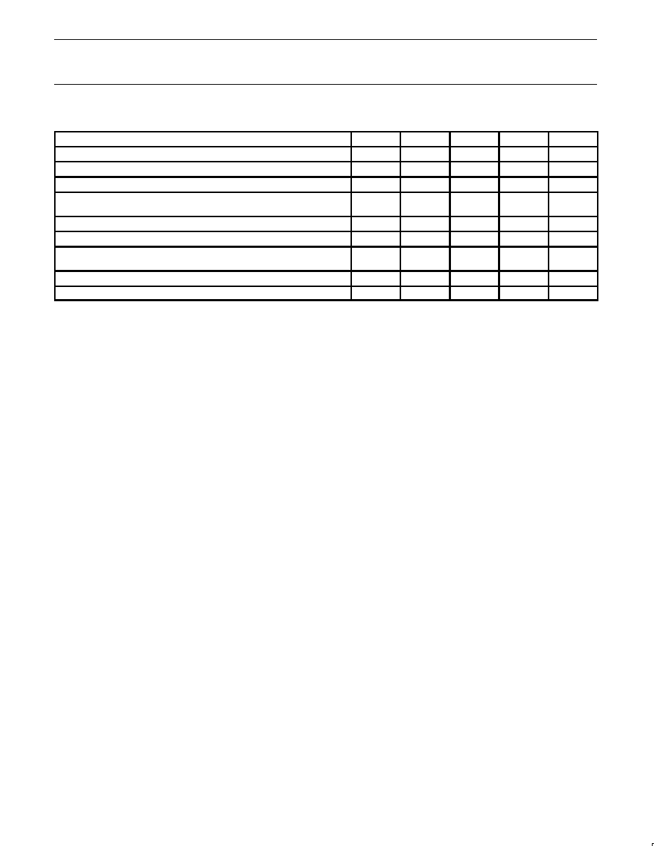
FEATURE SELECTION CHART
FEATURES
PCA9510
PCA9511
PCA9512
PCA9513
PCA9514
Idle detect
Yes
Yes
Yes
Yes
Yes
High impedance SDA, SCL pins for V
CC
= 0 V
Yes
Yes
Yes
Yes
Yes
Rise time accelerator circuitry on all SDA and SCL lines
--
Yes
Yes
Yes
Yes
Rise time accelerator circuitry hardware disable pin for lightly loaded
systems
--
--
Yes
--
--
Rise time accelerator threshold 0.8 V vs 0.6 V improves noise margin
--
--
--
Yes
Yes
Ready open drain output
Yes
Yes
--
Yes
Yes
Two V
CC
pins to support 5 V to 3.3 V level translation with improved noise
margins
--
--
Yes
--
--
1 V precharge on all SDA and SCL lines
IN only
Yes
Yes
--
--
92
µ
A current source on SCLIN and SDAIN for PICMG applications
--
--
--
Yes
--
OPERATION
Start-up
When the PCA9512 is powered up either V
CC
or V
CC2
may rise first
and either may be more positive or they may can be equal, however
the PCA9512 will not leave the under voltage lock out/initialization
state until both V
CC
and V
CC2
have gone above 2.5 V. If either V
CC
or V
CC2
drops below 2.0 V it will return to the under voltage lock
out/initialization state. In the under voltage lock out state the
connection circuitry is disabled, the rise time accelerators are
disabled, and the precharge circuitry is also disabled. After both V
CC
and V
CC2
are valid, independent of which is higher, the PCA9512
enters the initialization state, during this state the 1 V precharge
circuitry is activated and pulls up the SDA and SCL pins to 1 V
through individual 100 k
nominal resistors. At the end of the
initialization state the "Stop Bit And Bus Idle" detect circuit is
enabled. When all the SDA and SCL pins have been HIGH for the
bus idle time or when all pins are HIGH and a stop condition is seen
on the SDAIN and SCLIN pins, the connect circuitry is activated,
connecting SDAIN to SDAOUT and SCLIN to SCLOUT. The 1 V
precharge circuitry is disabled when the connection is made, unless
the ACC pin is LOW, the rise time accelerators are enabled at this
time also.
Connection Circuitry
Once the connection circuitry is activated, the behavior of SDAIN
and SDAOUT as well as SCLIN and SCLOUT become identical with
each acting as a bidirectional buffer that isolated the input bus
capacitance from the output bus capacitance while communicating
the logic levels. If V
CC
V
CC2
, then a level shifting function is also
performed between input and output. A LOW forced on either
SDAIN or SDAOUT will cause the other pin to be driven LOW by the
PCA9512. The same is also true for the SCL pins. Noise between
0.7V
CC
and V
CC
on the SDAIN and SCLIN pins and 0.7V
CC2
and
V
CC2
on the SDAOUT and SCLOUT pins is generally ignored
because a falling edge is only recognized when it falls below the
0.7V
CC
for SDAIN and SCLIN (or 0.7V
CC2
for SDAOUT and
SCLOUT pins) with a slew rate of at least 1.25 V/
µ
s. When a falling
edge is seen on one pin the other pin in the pair turns on a pull down
driver that is reference to a small voltage above the falling pin. The
driver will pull the pin down at a slow rate determined by the driver
and the load. The first falling pin may have a fast or slow slew rate, if
it is faster than the pull down slew rate then the initial pull down rate
will continue until it is LOW. If the first falling pin has a slow slew rate
then the second pin will be pulled down at its initial slew rate only
until it is just above the first pin voltage then they will both continue
down at the slew rate of the first. Once both sides are LOW they will
remain LOW until all the external drivers have stopped driving
LOWs. If both sides are being driven LOW to the same or nearly the
same value by external drivers, which is the case for clock
stretching and is typically the case for acknowledge, and one side
external driver stops driving, that pin will rise and rise above the
nominal offset voltage until the internal driver catches up and pulls it
back down to the offset voltage. This bounce is worst for low
capacitances and low resistances, and may become excessive.
When the last external driver stops driving a LOW, that pin will
bounce up and settle out just above the other pin as both rise
together with a slew rate determined by the internal slew rate control
and the RC time constant. As long as the slew rate is at least 1.25
V/
µ
s, when the pin voltage exceed 0.6 V the rise time accelerator
circuits are turned on and the pull down driver is turned off. If the
ACC pin is LOW the rise time accelerator circuits will be disabled
but the pull down driver will still turn off.
Philips Semiconductors
Product data sheet
PCA9512
Level shifting hot swappable I
2
C and SMBus buffer
2004 Oct 05
5
Maximum number of devices in series
Each buffer adds about 0.065 V dynamic level offset at 25
∞
C with
the offset larger at higher temperatures. Maximum offset (V
OS
) is
0.150 V. The LOW level at the signal origination end (master) is
dependent upon the load and the only specification point is the
I
2
C-bus specification of 3 mA will produce V
OL
< 0.4 V, although if
lightly loaded the V
OL
may be
0.1 V. Assuming V
OL
= 0.1 V and
V
OS
= 0.1 V, the level after four buffers would be 0.5 V, which is only
about 0.1 V below the threshold of the rising edge accelerator (about
0.6 V). With great care a system with four buffers may work, but as
the V
OL
moves up from 0.1 V, noise or bounces on the line will result
in firing the rising edge accelerator thus introducing false clock
edges. Generally it is recommended to limit the number of buffers in
series to two.
The PCA9510 (rise time accelerator is permanently disabled) and
the PCA9512 (rise time accelerator can be turned off) are a little
different with the rise time accelerator turned off because the rise
time accelerator will not pull the node up, but the same logic that
turns on the accelerator turns the pull-down off. If the V
IL
is above
0.6 V and a rising edge is detected, the pull-down will turn off and
will not turn back on until a falling edge is detected; so if the noise is
small enough it may be possible to use more than two PCA9510 or
PCA9512 parts in series but is not recommended.
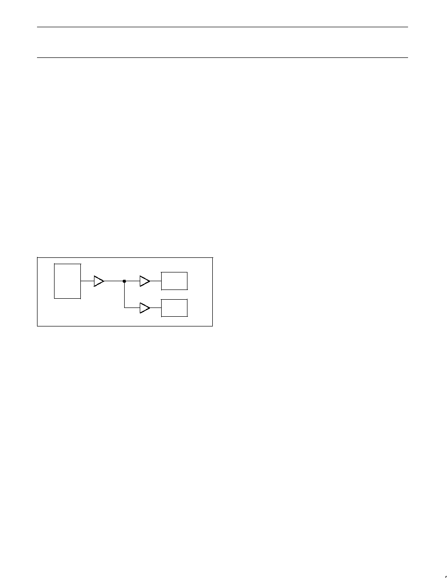
MASTER
buffer A
SLAVE B
buffer B
SLAVE C
buffer C
SW02353
common
node
Figure 4.
Consider a system with three buffers connected to a common node
and communication between the Master and Slave B that are
connected at either end of Buffer A and Buffer B in series as shown
in Figure 4. Consider if the V
OL
at the input of Buffer A is 0.3 V and
the V
OL
of Slave B (when acknowledging) is 0.4 V with the direction
changing from Master to Slave B and then from Slave B to Master.
Before the direction change you would observe V
IL
at the input of
Buffer A of 0.3 V and its output, the common node, is
0.4 V. The
output of Buffer B and Buffer C would be
0.5 V, but Slave B is
driving 0.4 V, so the voltage at Slave B is 0.4 V. The output of
Buffer C is
0.5 V. When the Master pull-down turns off, the input of
Buffer A rises and so does its output, the common node, because it
is the only part driving the node. The common node will rise to 0.5 V
before Buffer B's output turns on, if the pull-up is strong the node will
bounce. If the bounce goes above the threshold for the rising edge
accelerator
0.6 V the accelerators on both Buffer A and Buffer C
will fire contending with the output of Buffer B. The node on the input
of Buffer A will go HIGH as will the input node of Buffer C. After the
common node voltage is stable for a while the rising edge
accelerators will turn off and the common node will return to
0.5 V
because the Buffer B is still on. The voltage at both the Master and
Slave C nodes would then fall to
0.6 V until Slave B turned off. This
would not cause a failure on the data line as long as the return to
0.5 V on the common node (
0.6 V at the Master and Slave C)
occurred before the data setup time. If this were the SCL line, the
parts on Buffer A and Buffer C would see a false clock rather than a
stretched clock, which would cause a system error.
Propagation Delays
The delay for a rising edge is determined by the combined pull-up
current from the bus resistors and the PCA9512 and the effective
capacitance on the lines. If the pull-up currents are the same, any
difference in capacitance between the two sides. The t
PLH
may be
negative if the output capacitance is less than the input capacitance
and would be positive if the output capacitance is larger than the
input capacitance, when the currents are the same.
The t
PHL
can never be negative because the output does not start to
fall until the input is below 0.7V
CC
(or 0.7V
CC2
for SDAOUT and
SCLOUT) and the output pull down turn on has a nonzero delay,
and the output has a limited maximum slew rate and even it the
input slew rate is slow enough that the output catches up it will still
lag the falling voltage of the input by the offset voltage, The
maximum t
PHL
occurs when the input is driven LOW with zero delay
and the output is still limited by its turn on delay and the falling edge
slew rate, The output falling edge slew rate (which is a function of
temperature, V
CC
or V
CC2
, and process) as well as load current and
load capacitance.
Rise Time Accelerators
During positive bus transitions a 2 mA current source is switched on
to quickly slew the SDA and SCL lines HIGH once the input level of
0.6 V is exceeded. The rising edge rate should be at least 1.25 V/
µ
s
to guarantee turn on of the accelerators.
ACC Boost Current Enable
Users having lightly loaded systems may wish to disable the
rise-time accelerators. Driving this pin to ground turns off the
rise-time accelerators on all four SDA and SCL pins. Driving this pin
to the V
CC2
voltage enables normal operation of the rise-time
accelerators.
Philips Semiconductors
Product data sheet
PCA9512
Level shifting hot swappable I
2
C and SMBus buffer
2004 Oct 05
6
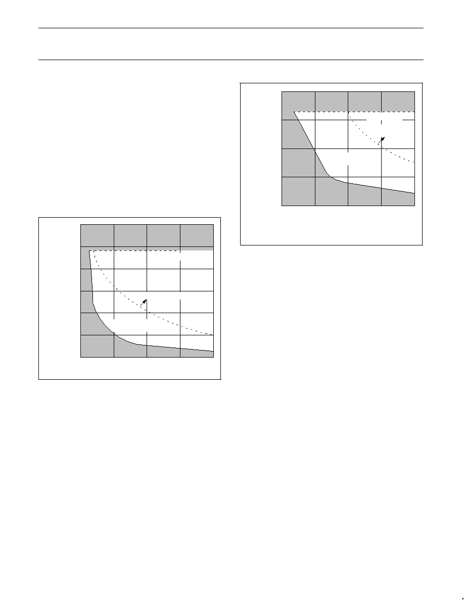
Resistor Pull-up Value Selection
The system pull-up resistors must be strong enough to provide a
positive slew rate of 1.25 V/
µ
s on the SDA and SCL pins, in order to
activate the boost pull-up currents during rising edges. Choose
maximum resistor value using the formula:
R
(V
CC(MIN)
≠ 0.6) (800,000)/C
where R is the pull-up resistor value in ohms, V
CC(MIN)
is the
minimum V
CC
voltage and C is the equivalent bus capacitance in
picofarads (pF).
In addition, regardless of the bus capacitance, always choose
R
16 k
for V
CC
= 5.5 V maximum, R
24 k
for V
CC
= 3.6 V
maximum. The start-up circuitry requires logic HIGH voltages on
SDAOUT and SCLOUT to connect the backplane to the card, and
these pull-up values are needed to overcome the precharge voltage.
See the curves in Figures 5 and 6 for guidance in resistor pull-up
selection.
30
20
15
21
5
0
0
100
200
300
400
C
BUS
(pF)
R
PULLUP
(k
)
25
RECOMMENDED
PULL-UP
R
MAX
= 24 k
RISE-TIME > 300 ns
SW02115
Figure 5. Bus requirements for 3.3 V systems
20
15
21
5
0
0
100
200
300
400
C
BUS
(pF)
R
PULLUP
(k
)
RECOMMENDED
PULL-UP
R
MAX
= 16 k
RISE-TIME
> 300 ns
SW02116
Figure 6. Bus requirements for 5 V systems
Minimum SDA and SCL Capacitance
Requirements
The device connection circuitry requires a minimum capacitance
loading on the SDA and SCL pins in order to function properly. The
value of this capacitance is a function of V
CC
and the bus pull-up
resistance. Estimate the bus capacitance on both the backplane and
the card data and clock buses, and refer to Figures 5 and 6 to
choose appropriate pull-up resistor values. Note from the figures
that 5 V systems should have at least 47 pF capacitance on their
buses and 3.3 V systems should have at least 22 pF capacitance for
proper operation of the PCA9512. Although the device has been
designed to be marginally stable with smaller capacitance loads, for
applications with less capacitance, provisions need to be made to
add a capacitor to ground to ensure these minimum capacitance
conditions if oscillations are noticed during initial signal integrity
verification.
Philips Semiconductors
Product data sheet
PCA9512
Level shifting hot swappable I
2
C and SMBus buffer
2004 Oct 05
7
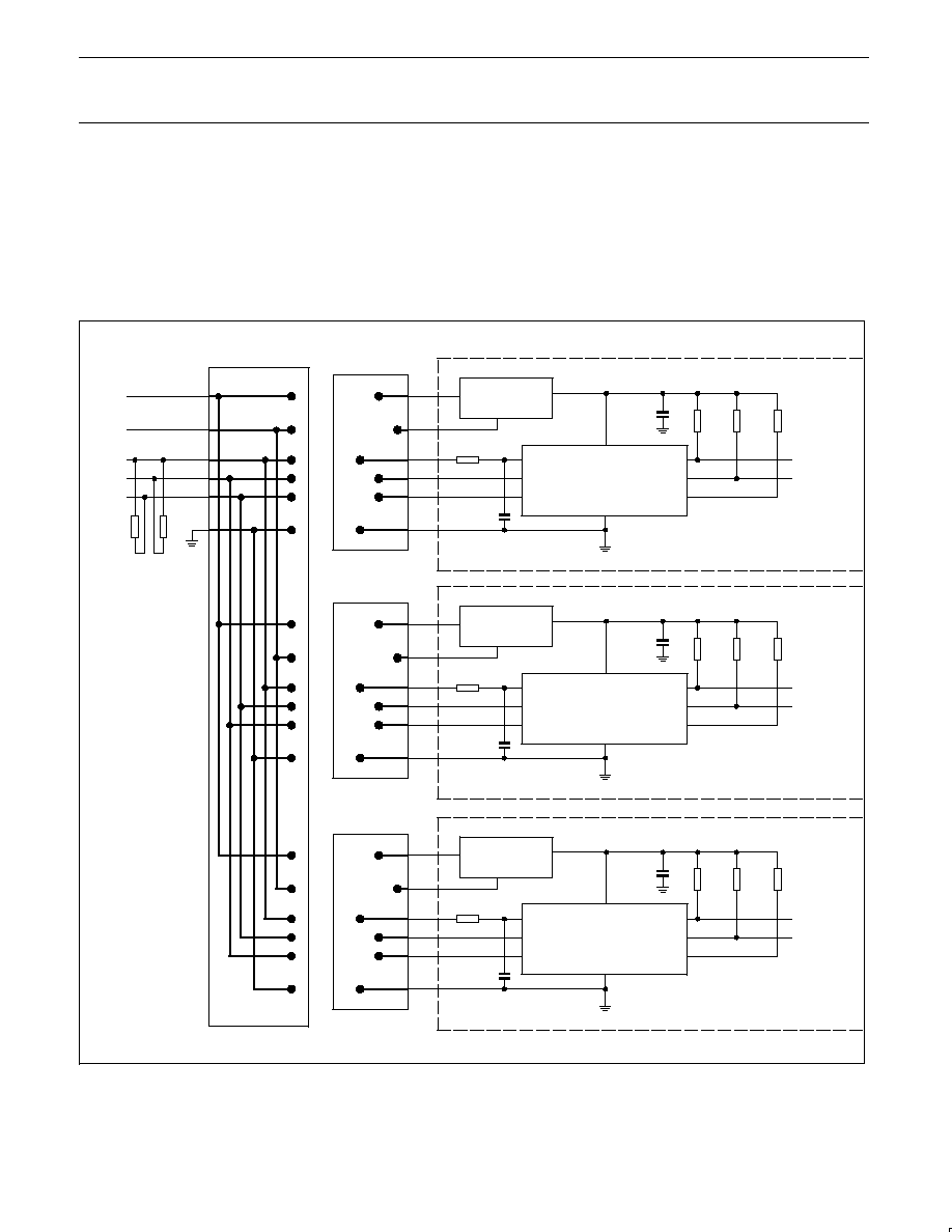
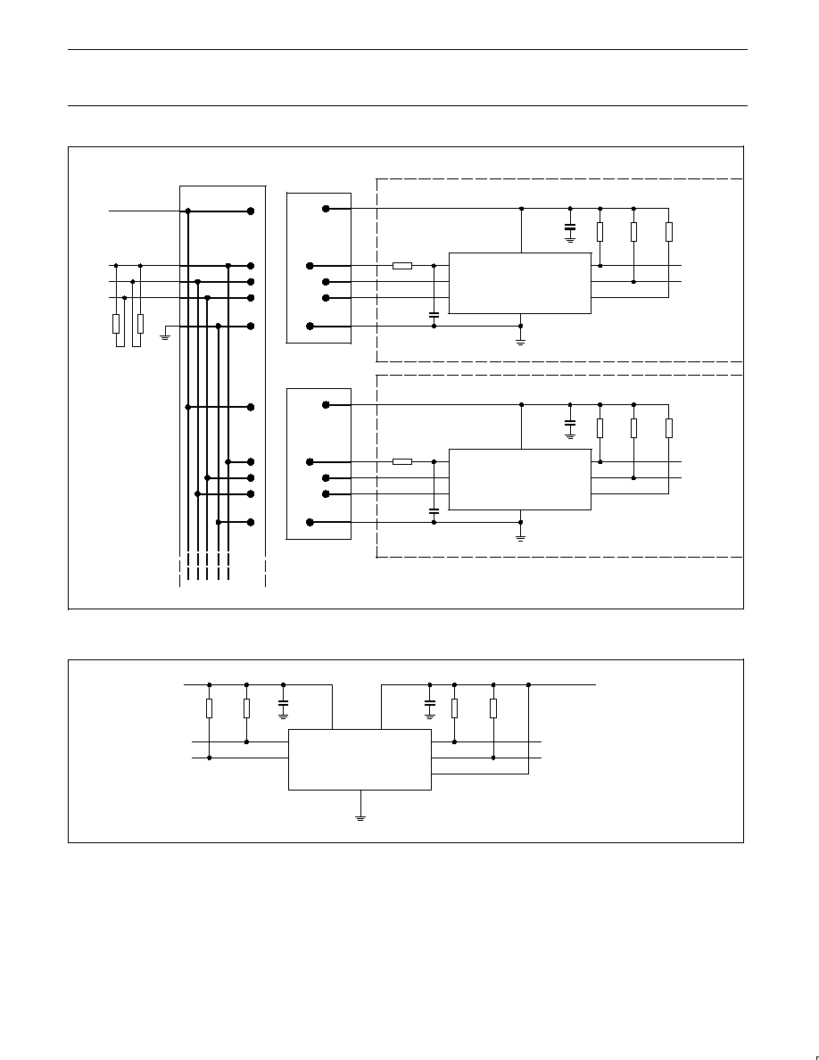
Hot Swapping and Capacitance Buffering
Application
Figures 7 through 9 illustrate the usage of the PCA9512 in
applications that take advantage of both its hot swapping and
capacitance buffering features. In all of these applications, note that
if the I/O cards were plugged directly into the backplane, all of the
backplane and card capacitances would add directly together,
making rise- and fall-time requirements difficult to meet. Placing a
PCA9512 on the edge of each card, however, isolates the card
capacitance from the backplane. For a given I/O card, the PCA9512
drives the capacitance of everything on the card and the backplane
must drive only the the capacitance of the bus buffer, which is less
than 10 pF, the connector, trace, and all additional cards on the
backplane.
See Application Note
AN10160, Hot Swap Bus Buffer for more
information on applications and technical assistance.
C1
0.01
µ
F
R4
10 k
R5
10 k
POWER SUPPLY
HOT SWAP
I/O PERIPHERAL CARD 1
R6
10 k
R3 5.1
C2
0.01
µ
F
V
CC
V
CC2
SDAIN
SCLIN
SDAOUT
SCLOUT
ACC
GND
CARD1_SDA
CARD1_SCL
PCA9512
C3
0.01
µ
F
R8
10 k
R9
10 k
POWER SUPPLY
HOT SWAP
I/O PERIPHERAL CARD 2
R10
10 k
R7 5.1
C4
0.01
µ
F
V
CC
V
CC2
SDAIN
SCLIN
SDAOUT
SCLOUT
ACC
GND
CARD2_SDA
CARD2_SCL
PCA9512
C5
0.01
µ
F
R12
10 k
R13
10 k
POWER SUPPLY
HOT SWAP
I/O PERIPHERAL CARD N
R14
10 k
C6
0.01
µ
F
V
CC
V
CC2
SDAIN
SCLIN
SDAOUT
SCLOUT
ACC
GND
CARDN_SDA
CARDN_SCL
PCA9512
R1
10 k
R2
10 k
V
CC2
V
CC
SDA
SCL
BD_SEL
BACKPLANE
BACKPLANE
CONNECTOR
SW02117
R11 5.1
ST
AGGERED CONNECT
OR
ST
AGGERED CONNECT
OR
ST
AGGERED CONNECT
OR
NOTE: Application assumes bus capacitance within "proper operation" region of Figures 5 and 6.
Figure 7. Hot swapping multiple I/O cards into a backplane using the PCA9512 in a CompactPCI, VME, and AdvancedTCA system
Philips Semiconductors
Product data sheet
PCA9512
Level shifting hot swappable I
2
C and SMBus buffer
2004 Oct 05
8
C1
0.01
µ
F
R4
10 k
R5
10 k
I/O PERIPHERAL CARD 1
R6
10 k
R3 5.1
C2
0.01
µ
F
V
CC
V
CC2
SDAIN
SCLIN
SDAOUT
SCLOUT
ACC
GND
CARD1_SDA
CARD1_SCL
PCA9512
C3
0.01
µ
F
R8
10 k
R9
10 k
I/O PERIPHERAL CARD 2
R10
10 k
R4 5.1
C4
0.01
µ
F
V
CC
V
CC2
SDAIN
SCLIN
SDAOUT
SCLOUT
ACC
GND
CARD2_SDA
CARD2_SCL
PCA9512
R1
10 k
R2
10 k
V
CC2
V
CC
SDA
SCL
BACKPLANE
BACKPLANE
CONNECTOR
SW02118
ST
AGGERED CONNECT
OR
ST
AGGERED CONNECT
OR
NOTE: Application assumes bus capacitance within "proper operation" region of Figures 5 and 6.
Figure 8. Hot swapping multiple I/O cards into a backplane using the PCA9512 with a custom connector
C1
0.01
µ
F
R3
10 k
R2
10 k
V
CC
V
CC2
SDAIN
SCLIN
SDAOUT
SCLOUT
ACC
GND
CARD_SDA
CARD_SCL
PCA9512
C2
0.01
µ
F
R4
10 k
R1
10 k
V
CC
5 V
CARD_V
CC
, 3 V
SCL
SCL
SW02119
NOTE: Application assumes bus capacitance within "proper operation" region of Figures 5 and 6.
Figure 9. 5 V to 3.3 V level translator and bus buffer
Philips Semiconductors
Product data sheet
PCA9512
Level shifting hot swappable I
2
C and SMBus buffer
2004 Oct 05
9
ABSOLUTE MAXIMUM RATINGS
Limiting values in accordance with the Absolute Maximum System (IEC 134).
Voltages with respect to pin GND.
LIMITS
SYMBOL
PARAMETER
MIN.
MAX.
UNIT
V
CC
Supply voltage range V
CC
≠0.5
+7
V
V
CC2
Supply voltage range V
CC2
≠0.5
+7
V
V
n
SDAIN, SCLIN, SDAOUT, SCLOUT, ACC
≠0.5
+7
V
I
I
Maximum current for inputs
≠
±
20
mA
I
IO
Maximum current for I/O pins
≠
±
50
mA
T
opr
Operating temperature range
≠40
+85
∞
C
T
stg
Storage temperature range
≠65
+125
∞
C
T
sld
Lead soldering temperature (10 sec max)
--
+300
∞
C
T
j(max)
Maximum junction temperature
--
+125
∞
C
NOTE:
1. Stresses beyond those listed may cause permanent damage to the device. These are stress ratings only and functional operation of the
device at these or any other conditions beyond those indicated under "recommended operating conditions" is not implied. Exposure to
absolute-maximum-rated conditions for extended periods may affect device reliability.
Philips Semiconductors
Product data sheet
PCA9512
Level shifting hot swappable I
2
C and SMBus buffer
2004 Oct 05
10
ELECTRICAL CHARACTERISTICS
V
CC
= 2.7 V to 5.5 V; T
amb
= ≠40
∞
C to +85
∞
C unless otherwise noted.
SYMBOL
PARAMETER
TEST CONDITIONS
LIMITS
UNIT
SYMBOL
PARAMETER
TEST CONDITIONS
MIN.
TYP.
MAX.
UNIT
Power supply
V
CC
Supply voltage
Note 1.
2.7
--
5.5
V
V
CC2
Card side supply voltage
Note 1.
2.7
--
5.5
V
I
VCCI
V
CC
supply current
V
CC
= 5.5 V; V
SDAIN
= V
SCLIN
= 0 V
--
1.2
3.6
mA
I
VCC2
V
CC
supply current
V
CC
= 5.5 V; V
SDAOUT
= V
SCLOUT
= 0 V
--
1.1
2.4
mA
Start-up circuitry
V
PRE
Precharge voltage
SDA, SCL floating; Note 1.
0.8
1.1
1.2
V
t
EN
Enable time on power-up
Note 6.
--
180
--
µ
s
t
IDLE
Bus idle time
Notes 1 and 7.
50
140
250
µ
s
Rise time accelerators
I
PULLUPAC
Transient boosted pull-up current
Positive transition on SDA, SCL,
ACC = 0.7 V
◊
V
CC2
; V
CC
= 2.7 V;
Slew rate = 1.25 V/
µ
s; Note 2.
1
2
--
mA
V
ACCDIS
Accelerator disable threshold
0.3
◊
V
CC2
0.5
◊
V
CC2
--
V
V
ACCEN
Accelerator enable threshold
--
0.5
◊
V
CC2
0.7
◊
V
CC2
V
I
VACC
A
CC
input current
≠1
±
0.1
1
µ
A
t
PDOFF
A
CC
delay, on/off
--
5
--
ns
Input≠output connection
V
OS
Input≠output offset voltage
10 k
to V
CC
on SDA, SCL;
V
CC
= 3.3 V, V
CC2
= 3.3 V;
V
IN
= 0.2 V; Note 1; Note 3.
0
70
150
mV
f
SCL_SDA
operating frequency
Guaranteed by design, not subject to
test
0
--
400
kHz
C
IN
Digital input capacitance
Guaranteed by design,
not subject to test
--
--
10
pF
V
OL
LOW-level output voltage
Input = 0 V. SDA, SCL pins;
I
SINK
= 3 mA; V
CC
= 2.7 V;
V
CC2
= 2.7 V; Note 1.
0
--
0.4
V
I
LI
Input leakage current
SDA, SCL pins = V
CC
= 5.5 V;
V
CC2
= 5.5 V
≠1
--
5
µ
A
Timing characteristics
f
I2C
I
2
C operating frequency
Note 4
0
--
400
kHz
t
BUF
Bus free time between stop and
start condition
Note 4
1.3
--
--
µ
s
t
HD;STA
Hold time after (repeated) start
condition
Note 4
0.6
--
--
µ
s
t
SU;STA
Repeated start condition setup
time
Note 4
0.6
--
--
µ
s
t
SU;STO
Stop condition setup time
Note 4
0.6
--
--
µ
s
t
HD;DAT
Data hold time
Note 4
300
--
--
ns
t
SU;DAT
Data setup time
Note 4
100
--
--
ns
t
LOW
Clock LOW period
Note 4
1.3
--
--
µ
s
t
HIGH
Clock HIGH period
Note 4
0.6
--
--
µ
s
t
f
Clock, data fall time
Notes 4 and 5
20 + 0.1
◊
C
B
--
300
ns
t
r
Clock, data rise time
Notes 4 and 5
20 + 0.1
◊
C
B
--
300
ns
NOTES:
1. This specification applies over the full operating temperature range.
2. I
PULLUPAC
varies with temperature and V
CC
voltage, as shown in the Typical Performance Characteristics section.

Philips Semiconductors
Product data sheet
PCA9512
Level shifting hot swappable I
2
C and SMBus buffer
2004 Oct 05
11
3. The connection circuitry always regulates its output to a higher voltage than its input. The magnitude of this offset voltage as a function of
the pull-up resistor and V
CC
voltage is shown in the Typical Performance Characteristics section.
4. Guaranteed by design, not production tested.
5. C
B
= total capacitance of one bus line in pF.
6. Enable time is from power-up of V
CC
and V
CC2
2.7 V to when idle or stop time begins.
7. Idle time is from when SDAx and SCLx are HIGH after enable time has been met.
TYPICAL PERFORMANCE CHARACTERISTICS
SW02343
TEMPERATURE (
∞
C)
≠40
+25
+85
1.5
1.3
1.1
0.9
0.7
I
CC
(mA)
1.4
1.2
1.0
0.8
V
CC
= 5.5 V
V
CC
= 2.7 V
V
CC
= 3.3 V
Figure 10. I
CC
versus Temperature (Note 1)
SW02346
TEMPERATURE (
∞
C)
≠40
+25
+85
12
8
4
0
I
PULLUP
AC
(mA)
10
6
2
V
CC
= 5 V
V
CC
= 2.7 V
V
CC
= 3.3 V
Figure 11. I
PULLUPAC
versus Temperature
V
CC
= 3.3 V
SW02344
TEMPERATURE (
∞
C)
≠40
+25
+85
460
t
PHL
(ns)
440
400
380
V
CC
= 2.7 V
V
CC
= 5.5 V
C
IN
= C
OUT
= 100 pF
R
PULLUPIN
= R
PULLUPOUT
= 10 k
420
Figure 12. Input≠output t
PHL
versus Temperature
SW02154
R
PULLUP
(
)
10,000
20,000
30,000
100
80
60
40
90
70
50
0
40,000
V
CC
= 3.3 V OR 5.5 V
V
OUT
≠ V
IN
(mV)
Figure 13. Connection circuitry V
OUT
≠ V
IN
NOTE:
1. I
CC2
(Pin 1) typical current averages 0.1 mA less than I
CC
on Pin 8.

Philips Semiconductors
Product data sheet
PCA9512
Level shifting hot swappable I
2
C and SMBus buffer
2004 Oct 05
12
TEST CIRCUIT
PULSE
GENERATOR
V
I
V
O
CL= 100 pF
V
CC
DEFINITIONS
R
L
=
Load resistor.
C
L
=
Load capacitance includes jig and probe capacitance
R
T
=
Termination resistance should be equal to the output
impedance Z
O
of the pulse generators.
V
CC
R
T
D.U.T.
R
L
= 10 k
SW02345
Figure 14. Test circuitry for switching times

Philips Semiconductors
Product data sheet
PCA9512
Level shifting hot swappable I
2
C and SMBus buffer
2004 Oct 05
13
SO8:
plastic small outline package; 8 leads; body width 3.9 mm
SOT96-1

Philips Semiconductors
Product data sheet
PCA9512
Level shifting hot swappable I
2
C and SMBus buffer
2004 Oct 05
14
TSSOP8:
plastic thin shrink small outline package; 8 leads; body width 3 mm
SOT505-1

Philips Semiconductors
Product data sheet
PCA9512
Level shifting hot swappable I
2
C and SMBus buffer
2004 Oct 05
15
REVISION HISTORY
Rev
Date
Description
_1
20041005
Product data sheet (9397 750 14005).
Philips Semiconductors
Product data sheet
PCA9512
Level shifting hot swappable I
2
C and SMBus buffer
2004 Oct 05
16
Purchase of Philips I
2
C components conveys a license under the Philips' I
2
C patent
to use the components in the I
2
C system provided the system conforms to the
I
2
C specifications defined by Philips. This specification can be ordered using the
code 9398 393 40011.
Definitions
Short-form specification -- The data in a short-form specification is extracted from a full data sheet with the same type number and title. For detailed information see
the relevant data sheet or data handbook.
Limiting values definition -- Limiting values given are in accordance with the Absolute Maximum Rating System (IEC 60134). Stress above one or more of the limiting
values may cause permanent damage to the device. These are stress ratings only and operation of the device at these or at any other conditions above those given
in the Characteristics sections of the specification is not implied. Exposure to limiting values for extended periods may affect device reliability.
Application information -- Applications that are described herein for any of these products are for illustrative purposes only. Philips Semiconductors make no
representation or warranty that such applications will be suitable for the specified use without further testing or modification.
Disclaimers
Life support -- These products are not designed for use in life support appliances, devices, or systems where malfunction of these products can reasonably be
expected to result in personal injury. Philips Semiconductors customers using or selling these products for use in such applications do so at their own risk and agree
to fully indemnify Philips Semiconductors for any damages resulting from such application.
Right to make changes -- Philips Semiconductors reserves the right to make changes in the products--including circuits, standard cells, and/or software--described
or contained herein in order to improve design and/or performance. When the product is in full production (status `Production'), relevant changes will be communicated
via a Customer Product/Process Change Notification (CPCN). Philips Semiconductors assumes no responsibility or liability for the use of any of these products, conveys
no license or title under any patent, copyright, or mask work right to these products, and makes no representations or warranties that these products are free from patent,
copyright, or mask work right infringement, unless otherwise specified.
Contact information
For additional information please visit
http://www.semiconductors.philips.com.
Fax: +31 40 27 24825
For sales offices addresses send e-mail to:
sales.addresses@www.semiconductors.philips.com.
©
Koninklijke Philips Electronics N.V. 2004
All rights reserved. Published in the U.S.A.
Date of release: 10-04
Document number:
9397 750 14005
Philips
Semiconductors
Data sheet status
[1]
Objective data
Preliminary data
Product data
Product
status
[2] [3]
Development
Qualification
Production
Definitions
This data sheet contains data from the objective specification for product development.
Philips Semiconductors reserves the right to change the specification in any manner without notice.
This data sheet contains data from the preliminary specification. Supplementary data will be published
at a later date. Philips Semiconductors reserves the right to change the specification without notice, in
order to improve the design and supply the best possible product.
This data sheet contains data from the product specification. Philips Semiconductors reserves the
right to make changes at any time in order to improve the design, manufacturing and supply. Relevant
changes will be communicated via a Customer Product/Process Change Notification (CPCN).
Data sheet status
[1] Please consult the most recently issued data sheet before initiating or completing a design.
[2] The product status of the device(s) described in this data sheet may have changed since this data sheet was published. The latest information is available on the Internet at URL
http://www.semiconductors.philips.com.
[3] For data sheets describing multiple type numbers, the highest-level product status determines the data sheet status.
Level
I
II
III