
1.
General description
The PCA9519 is a 4-channel level translating I
2
C-bus/SMBus repeater that enables the
processor low voltage 2-wire serial bus to interface with standard I
2
C-bus or SMBus I/O.
While retaining all the operating modes and features of the I
2
C-bus system during the
level shifts, it also permits extension of the I
2
C-bus by providing bidirectional buffering for
both the data (SDA) and the clock (SCL) lines, thus enabling the I
2
C-bus or SMBus
maximum capacitance of 400 pF on the higher voltage side. The SDA and SCL pins are
over-voltage tolerant and are high-impedance when the PCA9519 is unpowered.
The port B drivers are compliant with SMBus I/O levels, while port A uses a current
sensing mechanism to detect the input or output LOW signal which prevents bus lock-up.
The port A uses a 1 mA current source for pull-up and a 200
pull-down driver. This
results in a LOW on port A accommodating smaller voltage swings. The output pull-down
on the port A internal buffer LOW is set for approximately 0.2 V, while the input threshold
of the internal buffer is set about 50 mV lower than that of the output voltage LOW. When
the port A I/O is driven LOW internally, the LOW is not recognized as a LOW by the input.
This prevents a lock-up condition from occurring. The output pull-down on the port B
drives a hard LOW and the input level is set at 0.3 of SMBus or I
2
C-bus voltage level
which enables port B to connect to any other I
2
C-bus device or buffer.
The PCA9519 drivers are not enabled unless V
CC(A)
is above 0.8 V and V
CC(B)
is above
2.5 V. The enable (EN) pin can also be used to turn the drivers on and off under system
control. Caution should be observed to only change the state of the EN pin when the bus
is idle.
2.
Features
I
4-channel (4 SCL/SDA pairs), bidirectional buffer isolates capacitance and allows
400 pF on port B of the device
I
Voltage level translation from port A (1 V to V
CC(B)
-
1 V) to port B (3.0 V to 5.5 V)
I
Requires no external pull-up resistors on lower voltage port A
I
Active HIGH repeater enable input
I
Open-drain inputs/outputs
I
Lock-up free operation
I
Supports arbitration and clock stretching across the repeater
I
Accommodates Standard-mode and Fast-mode I
2
C-bus devices and multiple masters
I
Powered-off high-impedance I
2
C-bus pins
I
Operating supply voltage range of 1.0 V to V
CC(B)
-
1 V on port A, 3.0 V to 5.5 V on
port B
I
5 V tolerant B-side SCL and SDA and enable pins
PCA9519
4-channel level translating I
2
C-bus/SMBus repeater
Rev. 01 -- 22 June 2006
Objective data sheet

PCA9519_1
� Koninklijke Philips Electronics N.V. 2006. All rights reserved.
Objective data sheet
Rev. 01 -- 22 June 2006
2 of 17
Philips Semiconductors
PCA9519
4-channel level translating I
2
C-bus/SMBus repeater
I
0 Hz to 400 kHz clock frequency
Remark: The maximum system operating frequency may be less than 400 kHz
because of the delays added by the repeater.
I
ESD protection exceeds 2000 V HBM per JESD22-A114, 200 V MM per
JESD22-A115, and 1000 V CDM per JESD22-C101
I
Latch-up testing is done to JEDEC Standard JESD78 which exceeds 100 mA
I
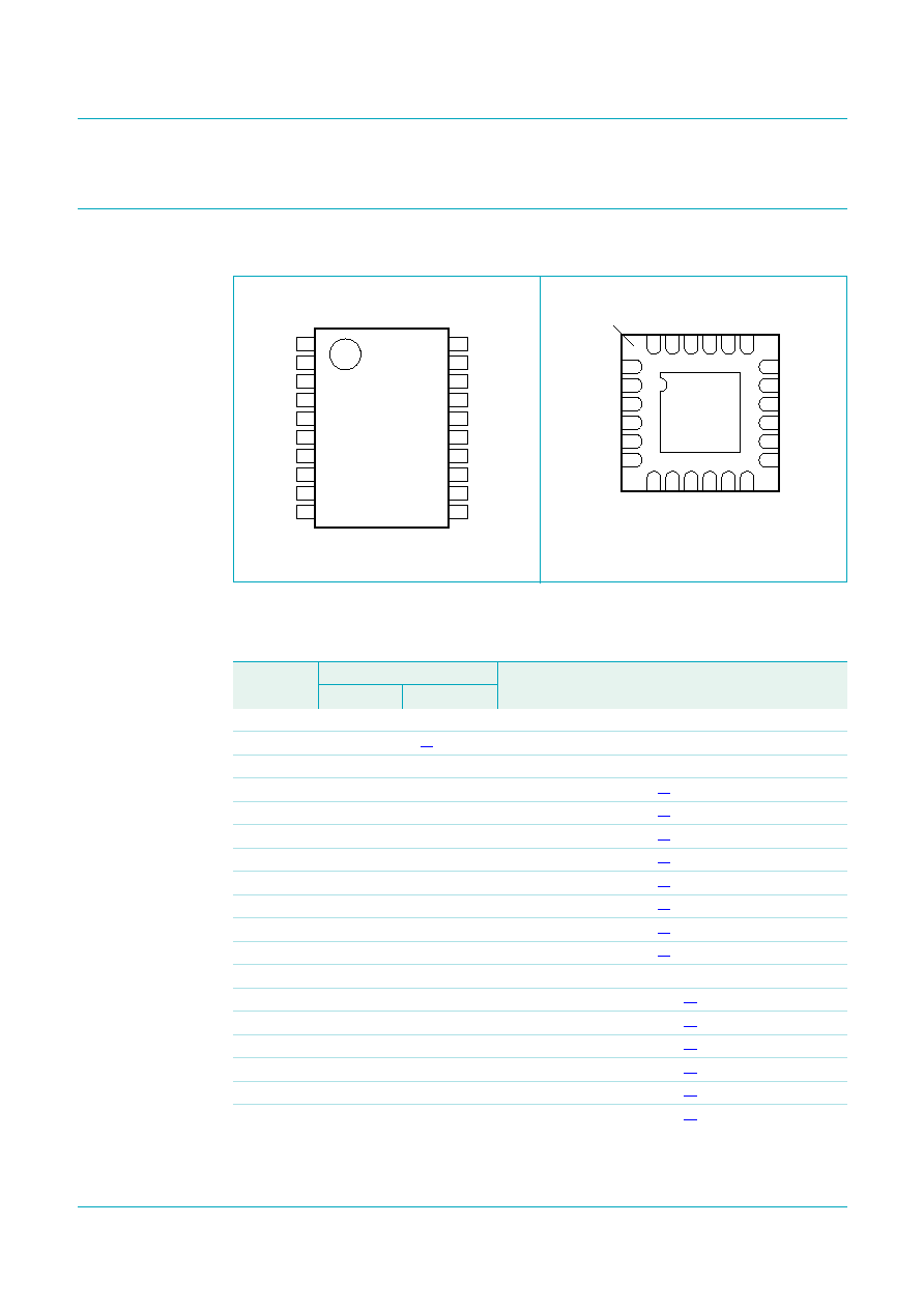
Packages offered: TSSOP20, HVQFN24
3.
Ordering information
4.
Functional diagram
Table 1.
Ordering information
Type number Topside
mark
Package
Name
Description
Version
PCA9519PW
PCA9519
TSSOP20
plastic thin shrink small outline package; 20 leads; body width 4.4 mm SOT360-1
PCA9519BS
9519
HVQFN24
plastic thermal enhanced very thin quad flat package; no leads;
24 terminals; body 4
�
4
�
0.85 mm
SOT616-1
Fig 1.
Functional diagram of PCA9519
002aab643
V
CC(A)
PCA9519
A1
A2
A8
EN
B1
B2
B8
V
CC(A)
V
CC(B)
GND
1 mA
V
CC(A)
1 mA
V
CC(A)
1 mA
PCA9519_1
� Koninklijke Philips Electronics N.V. 2006. All rights reserved.
Objective data sheet
Rev. 01 -- 22 June 2006
3 of 17
Philips Semiconductors
PCA9519
4-channel level translating I
2
C-bus/SMBus repeater
5.
Pinning information
5.1 Pinning
5.2 Pin description
Fig 2.
Pin configuration for TSSOP20
Fig 3.
Pin configuration for HVQFN24
PCA9519PW
EN
V
CC(B)
B1
A1
B2
A2
B3
A3
B4
A4
B5
A5
B6
A6
B7
A7
B8
A8
GND
V
CC(A)
002aab640
1
2
3
4
5
6
7
8
9
10
12
11
14
13
16
15
18
17
20
19
002aab641
PCA9519BS
Transparent top view
B7
A6
A7
B6
A5
B5
A4
B4
A3
B3
A2
B2
A8
n.c.
n.c.
V
CC(B)
EN
B8
A1
V
CC(A)
GND
n.c.
n.c.
B1
terminal 1
index area
6
13
5
14
4
15
3
16
2
17
1
18
7
8
9
10
11
12
24
23
22
21
20
19
Table 2.
Pin description
Symbol
Pin
Description
TSSOP20
HVQFN24
EN
1
11
enable input (active HIGH)
GND
10
22
[1]
ground (0 V)
V
CC(A)
11
23
port A power supply
A1
19
24
A1 port (low voltage side)
[2]
A2
18
1
A2 port (low voltage side)
[2]
A3
17
2
A3 port (low voltage side)
[2]
A4
16
3
A4 port (low voltage side)
[2]
A5
15
4
A5 port (low voltage side)
[2]
A6
14
5
A6 port (low voltage side)
[2]
A7
13
6
A7 port (low voltage side)
[2]
A8
12
7
A8 port (low voltage side)
[2]
V
CC(B)
20
10
port B power supply
B8
9
12
B8 port (SMBus/I
2
C-bus side)
[2]
B7
8
13
B7 port (SMBus/I
2
C-bus side)
[2]
B6
7
14
B6 port (SMBus/I
2
C-bus side)
[2]
B5
6
15
B5 port (SMBus/I
2
C-bus side)
[2]
B4
5
16
B4 port (SMBus/I
2
C-bus side)
[2]
B3
4
17
B3 port (SMBus/I
2
C-bus side)
[2]

PCA9519_1
� Koninklijke Philips Electronics N.V. 2006. All rights reserved.
Objective data sheet
Rev. 01 -- 22 June 2006
4 of 17
Philips Semiconductors
PCA9519
4-channel level translating I
2
C-bus/SMBus repeater
[1]
HVQFN package die supply ground is connected to both the GND pin and the exposed center pad. The
GND pin must be connected to supply ground for proper device operation. For enhanced thermal, electrical,
and board-level performance, the exposed pad needs to be soldered to the board using a corresponding
thermal pad on the board, and for proper heat conduction through the board thermal vias need to be
incorporated in the PCB in the thermal pad region.
[2]
Port A and port B can be used for either SCL or SDA.
6.
Functional description
Refer to
Figure 1 "Functional diagram of PCA9519"
.
The PCA9519 enables I
2
C-bus or SMBus translation down to V
CC(A)
as low as 1.0 V
without degradation of system performance. The PCA9519 contains 8 bidirectional
open-drain buffers specifically designed to support up-translation/down-translation
between the low voltage and 3.3 V SMBus or 5 V I
2
C-bus. Port B I/Os are over-voltage
tolerant to 5.5 V even when the device is unpowered.
The PCA9519 includes a power-up circuit that keeps the output drivers turned off until
V
CC(B)
is above 2.5 V and the V
CC(A)
is above 0.8 V. V
CC(B)
and V
CC(A)
can be applied in
any sequence at power-up. After power-up and with the EN pin HIGH, a LOW level on the
port A (below approximately 0.15 V) turns the corresponding port B driver (either SDA or
SCL) on and drives the port B down to about 0 V. When port A rises above approximately
0.15 V, the port B pull-down driver is turned off and the external pull-up resistor pulls the
pin HIGH. When the port B falls first and goes below 0.3V
CC(B)
, the port A driver is turned
on and the port A pulls down to 0.2 V (typical). The port B pull-down is not enabled unless
the port A voltage goes below V
ILc
. If the port A low voltage goes below V
ILc
, the port B
pull-down driver is enabled until the port A rises above approximately 0.15 V (V
ILc
), then
the port B, if not externally driven LOW, will continue to rise being pulled up by the
external pull-up resistor.
Remark: Ground offset between the PCA9519 ground and the ground of devices on
port A of the PCA9519 must be avoided.
The reason for this cautionary remark is that a CMOS/NMOS open-drain capable of
sinking 3 mA of current at 0.4 V will have an output resistance of 133
or less (R = E / I).
Such a driver will share enough current with the port A output pull-down of the PCA9519
to be seen as a LOW as long as the ground offset is zero. If the ground offset is greater
than 0 V, then the driver resistance must be less. Since V
ILc
can be as low as 90 mV at
cold temperatures and the low end of the current distribution, the maximum ground offset
should not exceed 50 mV.
Bus repeaters that use an output offset are not interoperable with port A of the PCA9519
as their output LOW levels will not be recognized by the PCA9519 as a LOW. If the
PCA9519 is placed in an application where the V
IL
of the port A of the PCA9519 does not
B2
3
18
B2 port (SMBus/I
2
C-bus side)
[2]
B1
2
19
B1 port (SMBus/I
2
C-bus side)
[2]
n.c.
-
8, 9, 20, 21
not connected
Table 2.
Pin description
...continued
Symbol
Pin
Description
TSSOP20
HVQFN24
PCA9519_1
� Koninklijke Philips Electronics N.V. 2006. All rights reserved.
Objective data sheet
Rev. 01 -- 22 June 2006
5 of 17
Philips Semiconductors
PCA9519
4-channel level translating I
2
C-bus/SMBus repeater
go below its V
ILc
it will pull the port B LOW initially when the port A input transitions LOW
but port B will return HIGH, so it will not reproduce the port A input on port B. Such
applications should be avoided.
Port B is interoperable with all I
2
C-bus slaves, masters, and repeaters.
6.1 Enable
The EN pin is active HIGH and allows the user to select when the repeater is active. This
can be used to isolate a badly behaved slave on power-up until after the system power-up
reset. It should never change state during an I
2
C-bus operation because disabling during
a bus operation will hang the bus and enabling part way through a bus cycle could
confuse the I
2
C-bus parts being enabled.
The enable pin should only change state when the bus and the repeater port are in an idle
state to prevent system failures.
6.2 I
2
C-bus systems
As with the standard I
2
C-bus system, pull-up resistors are required to provide the logic
HIGH levels on the buffered bus (standard open-collector configuration of the I
2
C-bus).
The size of these pull-up resistors depends on the system. Each of the port A I/Os has an
internal pull-up current source and does not require the external pull-up resistor. The
port B is designed to work with Standard mode and Fast mode I
2
C-bus devices in addition
to SMBus devices. Standard mode I
2
C-bus devices only specify 3 mA output drive; this
limits the termination current to 3 mA in a generic I
2
C-bus system where Standard mode
devices and multiple masters are possible. Under certain conditions higher termination
currents can be used.
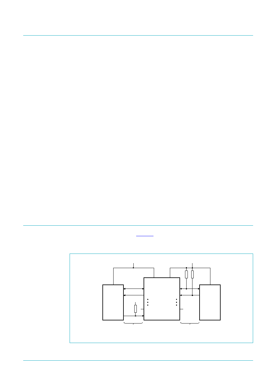
7.
Application design-in information
A typical application is shown in
Figure 4
. In this example, the CPU is running on a 1.1 V
I
2
C-bus while the master is connected to a 3.3 V bus. Both buses run at 400 kHz. Master
devices can be placed on either bus.
Fig 4.
Typical application
002aab642
V
CC(B)
V
CC(A)
PCA9519
A1
B1
A2
B2
EN
10 k
10 k
SDA
SCL
CPU
MASTER
400 kHz
SDA
SCL
bus A
bus B
3.3 V
A8
B8
1.1 V
10 k
1.1 V