 | –≠–ª–µ–∫—Ç—Ä–æ–Ω–Ω—ã–π –∫–æ–º–ø–æ–Ω–µ–Ω—Ç: PCD6001 | –°–∫–∞—á–∞—Ç—å:  PDF PDF  ZIP ZIP |
Document Outline
- 1 FEATURES
- 2 APPLICATION SUMMARY
- 3 GENERAL DESCRIPTION
- 4 ORDERING INFORMATION
- 5 BLOCK DIAGRAM
- 6 PINNING INFORMATION
- 6.1 Pinning
- 6.2 Pin description
- 6.3 Pin types
- 7 FUNCTIONAL DESCRIPTION
- 7.1 Architecture
- 7.2 I/O summary
- 7.3 Overview of functional description
- 8 POWER SUPPLY, RESET AND START-UP
- 8.1 Power supply
- 8.2 Reset and start-up
- 9 TICB - GENERATION AND SELECTION OF SYSTEM CLOCKS
- 9.1 Microprocessor, DSP, CODEC and IOM clock generation
- 9.2 System clocks
- 9.3 Real-Time Clock generation
- 10 THE MICROCONTROLLER
- 10.1 Microcontroller architecture
- 10.2 Memory mapping
- 10.3 SFR mapping
- 10.4 Microcontroller interrupts
- 10.5 Interface to DSP
- 10.6 Interface to Real-Time Clock (RTC)
- 10.7 Interface to the Memory Control Block (MCB)
- 10.8 The test registers CDTRx, PMTRx and TCTRL
- 10.9 Interface to Timing and Control Block (TICB)
- 10.10 Power and Interrupt Control Register (PCON)
- 10.11I2 C-bus
- 10.12 MSK modem
- 10.13 LE control
- 11 DSP I/O REGISTERS
- 12 EXTERNAL MEMORY INTERFACE
- 12.1 Supported flash memories
- 12.2 DTAM external interface during target debugging
- 13 THE CODECs
- 13.1 Definitions
- 13.2 CODEC architecture
- 14 ANALOG VOLTAGE REFERENCE (AVR)
- 14.1 Bandgap reference
- 14.2 Analog Voltage Source (AVS)
- 15 IOM
- 15.1 Features
- 15.2 Pin description
- 15.3 Functional description
- 15.4 IOM data buffers
- 15.5 IOM Control Register (IOMC)
- 15.6 Timing
- 16 EXTERNAL I/O INTERFACES
- 16.1 External analog interfaces
- 16.2 External digital Interfaces
- 17 ELECTRICAL CHARACTERISTICS
- 17.1 Limiting values
- 17.2 Supply characteristics
- 17.3 Digital I/O
- 17.4 Analog supplies and general purpose ADC and DAC
- 17.5 CODECs
- 18 APPLICATION DIAGRAMS
- 19 PACKAGE OUTLINE
- 20 SOLDERING
- 21 DATA SHEET STATUS
- 22 DEFINITIONS
- 23 DISCLAIMERS
- 24 PURCHASE OF PHILIPS I2C COMPONENTS
DATA SHEET
Product specification
Supersedes data of 2001 Feb 05
File under Integrated Circuits, IC17
2001 Apr 17
INTEGRATED CIRCUITS
PCD6001
Digital telephone answering
machine chip

2001 Apr 17
2
Philips Semiconductors
Product specification
Digital telephone answering machine chip
PCD6001
CONTENTS
1
FEATURES
2
APPLICATION SUMMARY
2.1
Metalink emulation
3
GENERAL DESCRIPTION
4
ORDERING INFORMATION
5
BLOCK DIAGRAM
6
PINNING INFORMATION
6.1
Pinning
6.2
Pin description
6.3
Pin types
7
FUNCTIONAL DESCRIPTION
7.1
Architecture
7.2
I/O summary
7.3
Overview of functional description
8
POWER SUPPLY, RESET AND START-UP
8.1
Power supply
8.2
Reset and start-up
9
TICB - GENERATION AND SELECTION OF
SYSTEM CLOCKS
9.1
Microprocessor, DSP, CODEC and IOM clock
generation
9.2
System clocks
9.3
Real-Time Clock generation
10
THE MICROCONTROLLER
10.1
Microcontroller architecture
10.2
Memory mapping
10.3
SFR mapping
10.4
Microcontroller interrupts
10.5
Interface to DSP
10.6
Interface to Real-Time Clock (RTC)
10.7
Interface to the Memory Control Block (MCB)
10.8
The test registers CDTRx, PMTRx and TCTRL
10.9
Interface to Timing and Control Block (TICB)
10.10
Power and Interrupt Control Register (PCON)
10.11
I
2
C-bus
10.12
MSK modem
10.13
LE control
11
DSP I/O REGISTERS
11.1
Interface to CODEC
12
EXTERNAL MEMORY INTERFACE
12.1
Supported flash memories
12.2
DTAM external interface during target
debugging
13
THE CODECs
13.1
Definitions
13.2
CODEC architecture
14
ANALOG VOLTAGE REFERENCE (AVR)
14.1
Bandgap reference
14.2
Analog Voltage Source (AVS)
15
IOM
15.1
Features
15.2
Pin description
15.3
Functional description
15.4
IOM data buffers
15.5
IOM Control Register (IOMC)
15.6
Timing
16
EXTERNAL I/O INTERFACES
16.1
External analog interfaces
16.2
External digital Interfaces
17
ELECTRICAL CHARACTERISTICS
17.1
Limiting values
17.2
Supply characteristics
17.3
Digital I/O
17.4
Analog supplies and general purpose ADC and
DAC
17.5
CODECs
18
APPLICATION DIAGRAMS
19
PACKAGE OUTLINE
20
SOLDERING
20.1
Introduction to soldering surface mount
packages
20.2
Reflow soldering
20.3
Wave soldering
20.4
Manual soldering
20.5
Suitability of surface mount IC packages for
wave and reflow soldering methods
21
DATA SHEET STATUS
22
DEFINITIONS
23
DISCLAIMERS
24
PURCHASE OF PHILIPS I
2
C COMPONENTS

2001 Apr 17
3
Philips Semiconductors
Product specification
Digital telephone answering machine chip
PCD6001
1
FEATURES
∑
Excellent speech quality at average:
2.6, 3.2 or 5.2 kbits/s compression rate
∑
Excellent background noise suppression for speech
quality improvement
∑
Speech compression rate selection: 2.6, 3.2 or
5.2 kbits/s
∑
Speech decompression rate selection: 2.6, 3.2 or
5.2 kbits/s
∑
Variable playback speed: 50%, 100% and 200% of real
time
∑
Voice prompt playback
∑
Philips International Language Library (PILL) support
tools available; coding at 2.6, 3.2 or 5.2 kbits/s
∑
Voice operated start message recording (VOX)
∑
Call progress detection by busy tone detection and
programmable silence detection
∑
Recording time of minimum 20 minutes in 4-Mbit flash
memory (at 3.2 kbits/s)
∑
Excellent true full-duplex handsfree performance
provided by Philips `phlux' algorithm
∑
On-hook caller ID detection according to Bell 202 and
V.23 standards, as well as DTMF caller ID support
∑
Caller Alerting Signal (CAS) - caller ID level 2
∑
Dual tone generation for DTMF, melody tones and
information tones
∑
Optional dial tone detection, and optional ringing
detection using hardware Caller Identification (CID)
interface
∑
DTMF detection (for remote control function) with local
echo canceller for high reliability
∑
Digital volume control
∑
Mixed digital/analog adaptive limit and/or level control of
audio input signals
∑
Programmable analog CODEC gain for easy interfacing
∑
Internal 80C51 microcontroller can operate as system
controller; with selectable operating frequencies
between 1 and 21 MHz
∑
Internal 80C51 microcontroller emergency operation
down to 2.2 V eliminates the need for external diallers in
telephone answering machine applications
∑
Standard 80C51 development tools allow fast design of
Man-Machine-Interface (MMI) features
∑
On-board Minimum Shift Keying (MSK) modem for
CT0/CT1 applications
∑
Two integrated differential bit stream Analog-to-Digital
Converters (ADCs) for high quality audio input
∑
Two integrated differential bitstream Digital-to-Analog
Converters (DACs) for high quality audio output
∑
Software selectable auxiliary CODEC input channel
∑
Up to 38 general purpose digital I/O lines (most of them
bidirectional) including I
2
C-bus, available for connection
to keyboard, display, line interface, etc.
∑
On-chip 2-channel time multiplexed 8-bit general
purpose ADC for e.g. parallel set detection and battery
voltage measurement
∑
On-chip 8-bit general purpose DAC for e.g. speaker
amplifier volume control
∑
Day and time stamp possibility using built-in Real-Time
Clock
∑
Flexible speech memory interface for connection of
several types of speech flash memory (serial, CAD or
parallel) and DRAM
∑
I
2
C master/slave bus for peripheral control or I
2
C-bus
speech memory access
∑
Extensive power management support for battery and
emergency operation, also allowing portable (voice
memo) applications
∑
Digital IOM A/u-law interface for Slave or Master mode
operation at various bit rates
∑
Emergency operation from telephone line power only;
microprocessor and DTMF generator continue to
operate in this mode
∑
On-chip software switchable supply voltage for electret
microphone
∑
Single low supply voltage (2.2 to 2.8 V)
∑
Built-in single low-frequency, low-power, crystal or
ceramic resonator oscillator and on-chip PLL to reduce
EMI
∑
Stand-alone operation with low cost PAL, NTSC and
DTMF crystals
∑
API providing flash memory management functions
such as speech, telephone or CID data storage
∑
Pin and software compatible with the PCD6002
OTP-device (see Application note for restrictions).

2001 Apr 17
4
Philips Semiconductors
Product specification
Digital telephone answering machine chip
PCD6001
2
APPLICATION SUMMARY
The PCD6001 can be used in various applications, some
of which are listed below. Refer to Chapter 18 for the
corresponding outline application diagrams.
∑
Stand-alone digital answering machine; with handsfree
∑
Feature phone with integrated digital answering
machine and full-duplex handsfree
∑
Dual-line digital answering machines
∑
Analog cordless applications such as CT0/1 base
stations; with handsfree and MSK modem function for
RF digital data transmission
∑
Portable voice memo recorders
∑
Automotive applications - car status announcements for
example
∑
Low-cost desktop video conferencing
∑
IOM master/slave interface to connect directly to digital
systems like ISDN and DECT.
2.1
Metalink emulation
Metalink emulation is supported with the standard
package.
3
GENERAL DESCRIPTION
The PCD6001 integrates all the digital and analog speech
management and processing functions required for a
feature-phone with integrated digital answering machine,
or a stand-alone digital answering machine into a single
low-cost chip.
Key hardware features which give the chip distinct
advantages in performance and application over
competitive solutions include:
∑
The flexibility to change the MMI
∑
An easy-to-program standard 80C51 microcontroller
with 32-kbyte internal ROM memory
∑
High 80C51 microprocessor power for system controller
functions of CT0/CT1 system control functions
∑
Up to 38 general purpose I/O lines for peripheral control
∑
I
2
C-bus interface
∑
Flexible flash memory control to interface to several
types of serial and parallel flash memory
∑
Two integrated 16-bit bitstream audio CODECs for true
full-duplex handsfree operation or dual-line stand-alone
answering machine operation
∑
Internal Digital Speech Processor (DSP) for excellent
`HARMONY' sinusoidal speech compression,
decompression and variable playback speed
∑
Embedded DTMF detection, call progress detection,
voice operated recording (VOX)
∑
High quality caller ID FSK demodulation and Caller
Alerting Signal (CAS) detection for CID level 2
∑
Two channel telephone line input for caller ID FSK and
audio interfacing.
Philips provides a sophisticated API running on the
internal 80C51, allowing product developers to design
their MMIs quickly to suit particular applications. The API
takes care of all flash memory and DSP management
tasks and can be enhanced on request.
For the pre-recorded voice prompts, the Philips
International Language Library (PILL) tools are available
for a standard multimedia PC platform under Windows 95.
These tools provide a way to compile a range of
multi-lingual voice prompts for efficient storage in the
speech (flash) memory. The PILL tools support various
languages and their grammar adaptations.
4
ORDERING INFORMATION
TYPE
NUMBER
PACKAGE
TEMPERATURE
RANGE (
∞
C)
NAME
DESCRIPTION
VERSION
PCD6001H
QFP80
plastic quad flat package; 80 leads (lead length 1.95 mm);
body 14
◊
20
◊
2.8 mm
SOT318-2
-
25 to +70
PCD6001U
U/10
sawn wafer on Film Frame Carrier (delivery as Known
Good Dies)
-
-
25 to +70

2001 Apr 17
5
Philips Semiconductors
Product specification
Digital telephone answering machine chip
PCD6001
5
BLOCK DIAGRAM
handbook, full pagewidth
MGT427
32 KBYTE
ROM
AND
EXTERNAL
INTERFACE
P4
I
2
C-
BUS
MCB
P2
P0
MICROCONTROLLER
80C51
PSEN
ALE, RDN, WRN
P4.3
3
2
11 to 4
80 to 73
72 to 65
62
1
64
63
ALE
EA
MA7 to MA0
P2.7 to P2.0
P0.7 to P0.0
P4.3
PSEN
WR
RD
55
RSTIN
54
TST
MSK
IOM
MICM
WATCHDOG
CODEC 2
(ANALOG)
CODEC 2
(DIGITAL)
MAIN and
AUX RAM
56
P4.0/LE
57
P4.1/FSK
58
P4.2/FSO
59
P4.4/FSI
60
P4.5/GPC
P1
14 to 18
P1.0/EX2 to
P1.4/EX6
19
P1.5
20
P1.6/SCL
21
P1.7/SDA
52
P3.7/
MIN/
DI
MA
P3
51
P3.6/
MOUT2/
FSC
50
P3.5/
T1
49
P3.4/
T0
48
P3.3/
EX1N
47
P3.2/
EX0N
46
P3.1/
MOUT1/
DCK
45
26
SPKRM
24
MICP
25
VMIC
ANALOG
VOLTAGE
REFERENCE
and SUPPLY
27
VBGP
29
VREF
30
DAOUT
GENERAL
PURPOSE
A/D and D/A
33
AD1IN
32
AD0IN
31
SPKRP
23
LIFMIN2
CODEC 1
(ANALOG)
CODEC 1
(DIGITAL)
36
LIFPIN
35
LIFMIN1
37
LIFPOUT
39
LIFMOUT
38
P3.0/
MOUT0/
DO
XTAL1
OSCILLATOR
and PLL
TICB
PCD6001
idle
events
µ
C_CLK
DMI
RSTANA
CLK
main bus
wake-up
DSPCLK
DSP
plus
ROM,
RAM
42
XTAL2
41
VSSA
VSSPLL
WAKE-UP
28
VDDA
VDDPLL
34
43
40
53
12
44
VSS3V1
VDD3V1
VSS3V2
VDD3V2
13
61
22
VSS3V3
VDD3V3
Fig.1 Block diagram.
2001 Apr 17
6
Philips Semiconductors
Product specification
Digital telephone answering machine chip
PCD6001
6
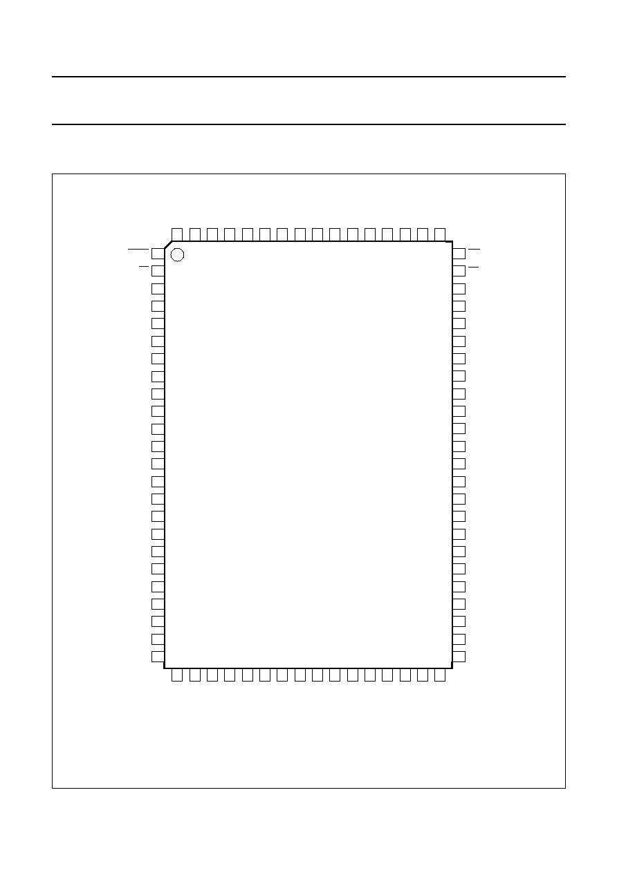
PINNING INFORMATION
6.1
Pinning
handbook, full pagewidth
PCD6001
MGT428
1
2
3
4
5
6
7
8
9
10
11
12
13
14
15
16
17
18
19
20
60
59
58
57
56
64
63
62
61
55
54
53
52
51
50
49
48
47
46
45
44
43
42
41
P4.5/GPC
P4.4/FSI
P4.2/FSO
P4.1/FSK
P4.0/LE
WR
RD
P4.3
VSS3V2
RSTIN
TST
VDD3V1
P3.7/MIN/DI
P3.6/MOUT2/FSC
P3.5/T1
P3.4/T0
P3.3/EX1N
P3.2/EX0N
P3.1/MOUT1/DCK
P3.0/MOUT0/DO
VDD3V3
VDDPLL
XTAL1
XTAL2
MA1
MA2
MA3
MA4
MA5
PSEN
EA
ALE
MA0
MA6
MA7
VDD3V2
VSS3V1
P1.0/EX2
P1.1/EX3
P1.2/EX4
P1.3/EX5
P1.4/EX6
P1.5
P1.6/SCL
P1.7/SDA
VSS3V3
SPKRP
SPKRM
21
22
23
24
25
26
27
28
29
30
31
32
33
34
35
36
37
38
39
40
MICP
MICM
V
MIC
V
SSA
V
BGP
V
REF
AD0IN
AD1IN
DAOUT
V
DDA
LIFPIN
LIFMIN2
LIFMIN1
LIFMOUT
LIFPOUT
V
SSPLL
P2.7
P2.6
P2.5
P2.4
P2.3
P2.2
P2.1
P2.0
P0.7
P0.6
P0.5
P0.4
P0.3
P0.2
P0.1
P0.0
80
79
78
77
76
75
74
73
72
71
70
69
68
67
66
65
Fig.2 Pin configuration.

2001 Apr 17
7
Philips Semiconductors
Product specification
Digital telephone answering machine chip
PCD6001
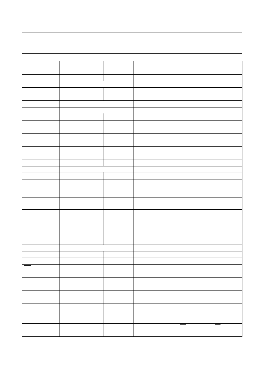
6.2
Pin description
Table 1
QFP80 package
SYMBOL
PIN
I/O
RESET
STATE
PIN TYPE
(1)
DESCRIPTION
PSEN
1
O
H
ucp4mthuwh
program store enable (80C51)
EA
2
I
Z
ucp4mthuwh
external access NOT (80C51)
ALE
3
O
H
ucp4mthuwh
address latch enable signal (80C51)
MA0
4
O
L
ops10c
general purpose output; EA = 1; add_low; EA = 0
MA1
5
O
L
ops10c
general purpose output; EA = 1; add_low; EA = 0
MA2
6
O
L
ops10c
general purpose output; EA = 1; add_low; EA = 0
MA3
7
O
L
ops10c
general purpose output; EA = 1; add_low; EA = 0
MA4
8
O
L
ops10c
general purpose output; EA = 1; add_low; EA = 0
MA5
9
O
L
ops10c
general purpose output; EA = 1; add_low; EA = 0
MA6
10
O
L
ops10c
general purpose output; EA = 1; add_low; EA = 0
MA7
11
O
L
ops10c
general purpose output; EA = 1; add_low; EA = 0
V
DD3V2
12
power supply
positive supply 2 (3.0 V) for digital circuitry
V
SS3V1
13
power supply
ground supply 1 for digital circuitry
P1.0/EX2
14
I/O
H
ucp4mthuwh
80C51 port pin/EX2 input
P1.1/EX3
15
I/O
H
ucp4mthuwh
80C51 port pin/EX3 input
P1.2/EX4
16
I/O
H
ucp4mthuwh
80C51 port pin/EX4 input
P1.3/EX5
17
I/O
H
ucp4mthuwh
80C51 port pin/EX5 input
P1.4/EX6
18
I/O
H
ucp4mthuwh
80C51 port pin/EX6 input
P1.5
19
I/O
H
ucp4mthuwh
80C51 port pin
P1.6/SCL
20
I/O
Z
I
2
C400k
80C51 port pin/I
2
C-bus clock
P1.7/SDA
21
I/O
Z
I
2
C400k
80C51 port pin/I
2
C-bus data
V
SS3V3
22
power supply
ground supply 3 for digital circuitry
SPKRP
23
O
Z
ana
positive output to speaker from CODEC2 (handsfree)
SPKRM
24
O
Z
ana
negative output to speaker from CODEC2 (handsfree)
MICP
25
I
0.625 V
ana
positive input from microphone to CODEC2 (handsfree)
MICM
26
I
0.625 V
ana
negative input from microphone to CODEC2 (handsfree)
V
MIC
27
O
Z
ana
positive microphone supply voltage (2 V)
V
SSA
28
power supply
ground supply voltage for analog circuits
V
BGP
29
O
1.25 V
band gap output voltage (V
BGP
)
V
REF
30
O
2.00 V
ana
reference voltage (V
REF
)
AD0IN
31
I
-
ana
analog input channel 1 for general purpose ADC
AD1IN
32
I
-
ana
analog input channel 2 for general purpose ADC
DAOUT
33
O
0.5V
DDA
ana
analog output channel for general purpose D/A converter
V
DDA
34
power supply
positive supply (2.5 V) for analog circuits
LIFPIN
35
I
0.625 V
ana
positive analog input of CODEC1 (line CODEC)
LIFMIN2
36
I
0.625 V
ana
negative analog input 2 of CODEC1 (line CODEC)
LIFMIN1
37
I
0.625 V
ana
negative analog input 1 of CODEC1 (line CODEC)
LIFMOUT
38
O
Z
ana
negative analog output of CODEC1 (line CODEC)
2001 Apr 17
8
Philips Semiconductors
Product specification
Digital telephone answering machine chip
PCD6001
LIFPOUT
39
O
Z
ana
positive analog output of CODEC1 (line CODEC)
V
SSPLL
40
power supply
ground supply for XTAL clock and PLL circuitry
XTAL2
41
O
running
ana
crystal oscillator output
XTAL1
42
I
-
ana
crystal oscillator input
V
DDPLL
43
power supply
positive supply (2.5 V) for XTAL clock and PLL circuitry
V
DD3V3
44
power supply
positive supply 3 (3.0 V) for digital circuitry
P3.0/MOUT0/DO
45
I/O
H
ucp4mthuwh
80C51 port pin/MSK output 0/IOM data output
P3.1/MOUT/DCK
46
I/O
H
ucp4mthuwh
80C51 port pin/MSK output 1/IOM DCK signal
P3.2/EX0N
47
I/O
H
ucp4mthuwh
80C51 port pin/EX0N input
P3.3/EX1N
48
I/O
H
ucp4mthuwh
80C51 port pin/EX1N input
P3.4/T0
49
I/O
H
ucp4mthuwh
80C51 port pin/Timer 0 input
P3.5/T1
50
I/O
H
ucp4mthuwh
80C51 port pin/Timer 1 input
P3.6/MOUT2/FSC
51
I/O
H
ucp4mthuwh
80C51 port pin/MSK output 2/IOM FSC signal
P3.7/MIN/DI
52
I/O
H
ucp4mthuwh
80C51 port pin/MSK input/IOM data input
V
DD3V1
53
power supply
positive supply 1 (2.5 V) for digital circuitry
TST
54
I
-
iptd
test input (recommended to be connected to ground)
RSTIN
55
I
-
ipth
reset in
P4.0/LE
56
I/O
L
ucp4mthuwh
general purpose I/O/LCD enable, configured as OD after
reset
P4.1/FSK
57
I/O
Z
ucp4mthuwh
general purpose I/O/Flash Serial Clock, configured
as OD after reset
P4.2/FSO
58
I/O
Z
ucp4mthuwh
general purpose I/O/Flash Serial Out, configured as OD
after reset
P4.4/FSI
59
I/O
Z
ucp4mthuwh
general purpose I/O/Flash Serial In, configured as OD
after reset
P4.5/GPC
60
I/O
L
ucp4mthuwh
general purpose I/O/GP clock output (crystal clock or
microcontroller clock), configured as OD after reset
V
SS3V2
61
power supply
negative supply 2 (ground) for digital circuitry
P4.3
62
I/O
Z
ucp4mthuwh
general purpose I/O, configured as OD after reset
RD
63
O
Z
ucp4mthuwh
80C51 read NOT, configured as OD after reset
WR
64
O
Z
ucp4mthuwh
80C51 write NOT, configured as OD after reset
P0.0
65
I/O
Z
uceda4mtuwh 80C51 Port 0 input/output
P0.1
66
I/O
Z
uceda4mtuwh 80C51 Port 0 input/output
P0.2
67
I/O
Z
uceda4mtuwh 80C51 Port 0 input/output
P0.3
68
I/O
Z
uceda4mtuwh 80C51 Port 0 input/output
P0.4
69
I/O
Z
uceda4mtuwh 80C51 Port 0 input/output
P0.5
70
I/O
Z
uceda4mtuwh 80C51 Port 0 input/output
P0.6
71
I/O
Z
uceda4mtuwh 80C51 Port 0 input/output
P0.7
72
I/O
Z
uceda4mtuwh 80C51 Port 0 input/output
P2.0
73
O
L
ucp4mthuwh
general purpose output, EA = 1; add_high; EA = 0
P2.1
74
O
L
ucp4mthuwh
general purpose output, EA = 1; add_high; EA = 0
SYMBOL
PIN
I/O
RESET
STATE
PIN TYPE
(1)
DESCRIPTION

2001 Apr 17
9
Philips Semiconductors
Product specification
Digital telephone answering machine chip
PCD6001
Note
1. The pin type codes are explained in Section 6.3.
P2.2
75
O
L
ucp4mthuwh
general purpose output, EA = 1; add_high; EA = 0
P2.3
76
O
L
ucp4mthuwh
general purpose output, EA = 1; add_high; EA = 0
P2.4
77
O
L
ucp4mthuwh
general purpose output, EA = 1; add_high; EA = 0
P2.5
78
O
L
ucp4mthuwh
general purpose output, EA = 1; add_high; EA = 0
P2.6
79
O
L
ucp4mthuwh
general purpose output, EA = 1; add_high; EA = 0
P2.7
80
O
L
ucp4mthuwh
general purpose output, EA = 1; add_high; EA = 0
SYMBOL
PIN
I/O
RESET
STATE
PIN TYPE
(1)
DESCRIPTION
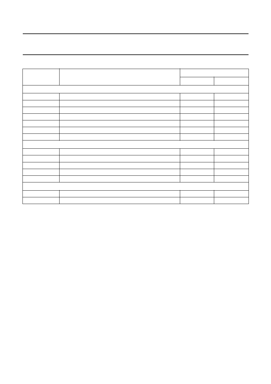
6.3
Pin types
6.3.1
P
OWER SUPPLY PINS
There are 6 different power supply domains (see Fig.3):
∑
Digital core circuit (2.5 V): V
DD3V1
/V
SS3V1
∑
Digital periphery circuit (3.0 V): V
DD3V2
/V
SS3V2
and
V
DD3V3
/V
SS3V3
∑
PLL circuits and crystal oscillator (2.5 V): V
DDPLL
and
V
SSPLL
∑
Analog circuits (2.5 V): V
DDA
and V
SSA
.
All V
SS
pins must be connected to the same ground plane
on the Printed-Circuit Board (PCB). All 2.5 V V
DD
pins
must be connected to the same power supply. All V
DD
pins
have to be separately decoupled, according to Chapter 18.
6.3.2
A
NALOG PINS
∑
ana: full ESD protected analog I/O pad (double
protection diode).
6.3.3
D
IGITAL PINS
∑
ucp4mthuwh: 4 mA 80C51 I/O pins
∑
uceda4mtuwh: 4 mA 80C51 I/O pins with input enable
∑
iptd: input pad buffer; pull-down
∑
ipth: input pad buffer with Schmitt trigger
∑
ops10c: output pad; push-pull; 4 mA output drive; 10 ns
slew control
∑
I
2
C400k: bidirectional open-drain I
2
C-bus compatible
pad.
handbook, halfpage
MGT429
VDD3V1
VSS3V1
VDD3V2
VSS3V2
VDD3V3
VSS3V3
VDDPLL
VSSPLL
VDDA
VSSA
Fig.3 PCD6001 chip supply rails with protection diodes.

2001 Apr 17
10
Philips Semiconductors
Product specification
Digital telephone answering machine chip
PCD6001
7
FUNCTIONAL DESCRIPTION
7.1
Architecture
The PCD6001 architecture is based on an embedded 8-bit
80C51 microcontroller, a Philips `REAL' DSP core, two
high quality AD/DA CODECs and a 32-kbyte ROM
microcontroller memory. Refer to the block diagram in
Chapter 5.
The most important DSP peripherals are the:
∑
CODECs
∑
DSP program ROM
∑
DSP RAM
∑
IOM interface.
The most important microcontroller peripherals are the:
∑
Memory Control Block (MCB)
∑
Watchdog Timer
∑
General purpose ports
∑
I
2
C-bus interface
∑
MSK block (used for digital data transfer and analogue
cordless applications).
The MCB, through Ports P0, P2, P4 and Memory
Address (MA) can interface to various types of flash
memory including serial, parallel or multiplexed
command/address/data. Most of the peripherals are
controlled via microcontroller special function registers.
The microcontroller initializes and controls the:
∑
DSP via the DSP to Microcontroller Interface (DMI)
∑
Speech flash memory via the Memory Control
Block (MCB), and P0/P4 port pins
∑
Clock and power settings via the Timing and Control
Block (TICB)
∑
Analog section via its Special Function Registers (SFR).
7.2
I/O summary
All digital I/O for peripherals such as keyboard, display,
line interface and others are handled by the
microcontroller via ports P0, P1, P2, P3, P4, and MA.
Port 2 and MA provide 16 general purpose output-only
lines (not bit-addressable, push-pull, 4 mA) to drive
peripherals. These ports can be used for peripheral control
if EA is logic 1. The 4 mA driving level should be adequate
to drive a low power LED directly if required.
In addition to these 16 output-only lines, 16 general
purpose I/O lines are provided by Ports 1 and 3. Port 1
can handle 5 external interrupts (P1.0 to P1.4) that are
also HIGH/LOW interrupt level programmable. Port 1 also
contains the I
2
C-bus. Port 3 can handle an additional
2 external interrupts (P3.2 and P3.3) which are active
LOW only. The Timer 0 and Timer 1 inputs are available
on Port 3 as for the standard 80C51. Ports 1 and 3 are
80C51 weak pull-up I/O lines with a 4 mA sink capability,
with the exception of the I
2
C-bus lines P1.6 and P1.7
which are open-drain. If the P3 alternate port function for
the MSK modem is chosen then the standard I/O is not
available on pins P3.0, P3.1, P3.6 and P3.7.
Port 4 lines are 6 more general purpose I/O. They will be
configured as open-drain after reset. These open-drains
can be connected via pull-up resistors to the telephone
system supply or to the mains AC supply. If a flash
memory with a different supply voltage (V
DD_FLASH
up
to 3.3 V) is connected, P4.3 can be pulled-up to this
voltage. This is required such that the Chip Enable
Not (CEN) input of a flash device is equal to V
DD_FLASH
to
reduce the standby power consumption. All other Port 4
pins should not be pulled up to a voltage higher than
V
DD_DTAM
.
In case a CAD flash is used, P4.4 and P4.5 are free
bit-addressable ports.
All P4 pins also can be configured to push-pull via the
register P4CFG. This brings the total of I/O lines to 38 (of
which 16 are output only).
In case an I
2
C-bus LCD driver is used, P4.0, at which
a Latch Enable (LE) function is provided for 68xxx family
microcontroller peripherals, is an additional free
bit-addressable open-drain I/O port.
The analog interfacing for the PCD6001 consists of the
analog audio I/O of the 2 CODECs and 2 additional
general purpose analog-to-digital inputs and a general
purpose digital-to-analog output for voltage measurement
and control respectively. Furthermore a stabilized
microphone supply output V
MIC
is provided which can be
switched on/off for power control.
One audio CODEC is dedicated for the PSTN line
communication (CODEC1). This line CODEC has a
differential low ohmic analog output which consists of
LIFPOUT and LIFMOUT. In case only one of the
differential outputs is used, LIFPOUT should be chosen,
since the Emergency mode DTMF signal is also available.

2001 Apr 17
11
Philips Semiconductors
Product specification
Digital telephone answering machine chip
PCD6001
The line CODEC has 3 inputs which are configurable as
2 single-ended inputs LIFMIN1 and LIFMIN2 that can be
selected by software control, while LIFPIN is AC coupled
to ground. It is also possible to use one of the LIFMIN
inputs (leaving the other unconnected) in conjunction with
the LIFPIN input as a differential input, in case a high
CMRR is required.
The second CODEC is dedicated for a local microphone
and loudspeaker connection (CODEC2). This handsfree
CODEC has a differential low ohmic analog output which
consists of SPKRP and SPKRM. This output can be used
either differential or single ended. The speaker output
impedance and driving level is not suitable to directly
connect a speaker. The handsfree CODEC has a
differential microphone input which consists of MICP and
MICM. This differential input features a fixed 16 dB
microphone preamplifier.
Both the line and handsfree CODEC outputs have on-chip
filtering for out of band signals such that no external filters
are required.
There are 2
◊
8-bit analog-to-digital inputs AD0IN and
AD1IN for voltage measurements which can be used for
parallel set detection algorithms or battery control. An 8-bit
DAC output DAOUT can provide an analog peripheral
control signal.
7.3
Overview of functional description
The detailed functional description is divided into separate
chapters covering the major functional blocks, as follows:
Chapter 8 "Power supply, reset and start-up"
Chapter 9 "TICB - generation and selection of system
clocks"
Chapter 10 "The microcontroller"
Chapter 11 "DSP I/O registers"
Chapter 12 "External memory interface"
Chapter 13 "The CODECs"
Chapter 16 "External I/O interfaces".
8
POWER SUPPLY, RESET AND START-UP
8.1
Power supply
The PCD6001 core circuitry is supplied by three 3 V supply
pairs. The crystal oscillator and PLL are supplied with a
separate pair of supply pins to provide a `clean' supply
voltage required for low jitter. The following supplies exist:
V
DD3V1
and V
SS3V1
: digital core supply 1 (2.5 V)
V
DD3V2
and V
SS3V2
: digital supply 2 (3.0 V)
V
DD3V3
and V
SS3V3
: digital supply 3 (3.0 V)
V
DDA
and V
SSA
: analog supply (2.5 V)
V
DDPLL
and V
SSPLL
: crystal clock and PLL supply (2.5 V).
8.2
Reset and start-up
After applying the power supply voltage, the chip will need
an external Power-on reset via pin RSTIN. RSTIN should
remain active (logic 1) until V
trh
and has to become active
again before the power supply drops below V
trl
.
The reset via RSTIN is one of 3 possible ways to perform
a reset. The following reset conditions exist:
∑
Wake-up from system off (crystal is off, but power is on)
by an external interrupt
∑
RSTIN, reset in from pin RSTIN
∑
Watchdog Timer expires.
After a Power-on reset and after a wake-up from system
off, a counter is activated, which guarantees that the first
instruction fetch of the microcontroller is delayed by at
least 4096 clock cycles.
To reduce power consumption during reset, the following
reset strategy is used. If the DSP function is not required,
it can be switched off by the microcontroller. The DSP
reset will then be delayed (until it is switched on again), in
order to avoid a large (reset) power consumption.

2001 Apr 17
12
Philips Semiconductors
Product specification
Digital telephone answering machine chip
PCD6001
9
TICB - GENERATION AND SELECTION OF
SYSTEM CLOCKS
The TICB generates the clocks for all digital chip blocks,
and controls the on/off switching of these blocks by using
clock gating. The TICB is controlled via the microcontroller
SFR registers SYMOD, CKCON and SPCON. The TICB
contains:
∑
An input section to adapt to different input clock rates
∑
A clock generation section
∑
A clock selection section
∑
The Real-Time Clock for a 1 minute interrupt generation
∑
The microcontroller interrupt timers (FS_event and
TIME_event) and the DSP interrupt timer (FS1) to
respectively synchronize the microcontroller and DSP
processes.
9.1
Microprocessor, DSP, CODEC and IOM clock
generation
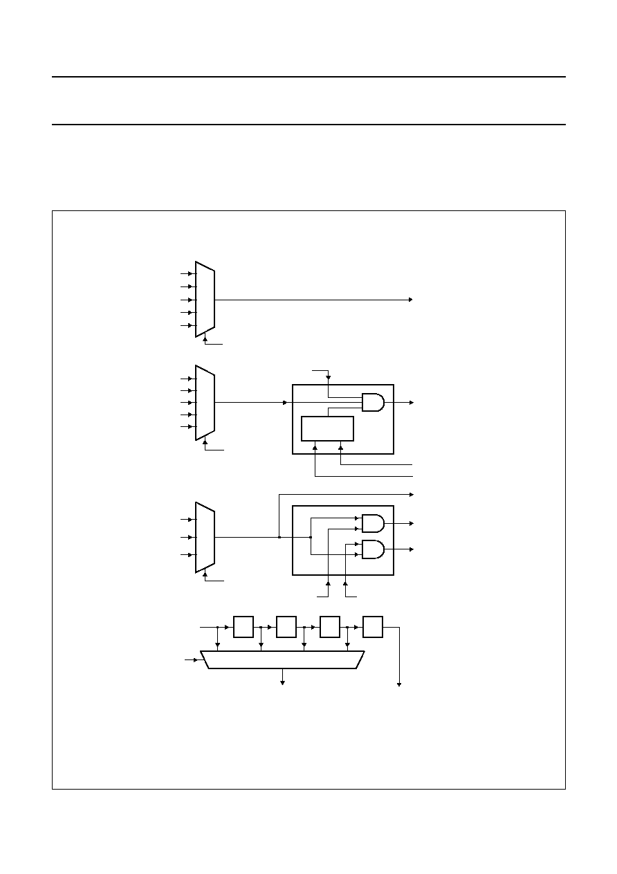
Figure 4 shows the TICB input section and the clock
generation section.
The clock generation section contains a PLL to generate
the clock rates which are higher then the input clock rate.
With the input section, a wider variety of input clock
frequencies can be adapted to the input frequency values
needed by the PLL (3.456 or 3.580 MHz).
In order to save power the PLL can be switched off. This
should however only be done when the chip is in the
Emergency mode. When switching on the PLL, it takes
40
µ
s (173 emergency clock periods) until the clock
frequencies are derived from the PLL output.
Table 2 gives a description of the signals and their values
for a crystal frequency of 3.456 and 3.580 MHz.
The clock generation section also contains logic to
synchronize the CODEC timing signals and the DSP and
microcontroller interrupt timers to an external Frame
Sync. (FSC). This synchronization is only activated when
using the IOM in Slave mode. If the IOM is activated in
Master mode, the TICB generates the DCK and
FSC signals from CLK28.
Some of the clock signals can be made available as
general purpose clock, for various peripherals needing a
clock source such as an PCA1070 line interface. This
general purpose clock (GPC) signal is an alternative
output of P4.5 and can be turned on with ALTP bit 3. With
ALTP bit 2, the source for GPC can be defined. The GPC
source is EMG_CLK (normally 3.58 MHz) when bit 2 is
logic 0 and the GPC source is
µ
C_CLK when bit 2 is set to
logic 1. As a spike-free GPC is not guaranteed when
switching between these clocks, it is recommended to first
set the clock source before switching on the GPC. The
ALTP register is described in more detail in Section 16.2.

2001 Apr 17
13
Philips Semiconductors
Product specification
Digital telephone answering machine chip
PCD6001
handbook, full pagewidth
MGT430
˜
2
˜
2
˜
6
˜
24
˜
3
˜
4
˜
192
DCK
GENERATOR
CLK3GEN
control and synchronization
CODEC timing signals
CLK_21
CLK_3
CDCCNTRL
EMG_CLK
PLL
◊
24
on
CLK_IN
SYMOD[5]
PLL_ON
CLK_28
CLK_21
CLK_14
0
1
CLK_7
CLK_1
CLK3_EMG
FSC
DCK
CLK_3
FS1
˜
2
CLK_42
˜
2
˜
4
SYMOD[5]
PLL_ON
SYMOD[6 or 7]
PLL_IN
20.736 MHz
for a 3.456 MHz
PLL input clock
CLK3_CORR
CLK3_OUT
CKCON[6 or 7]
Fig.4 TICB input section and clock generation.
2001 Apr 17
14
Philips Semiconductors
Product specification
Digital telephone answering machine chip
PCD6001
Table 2
Descriptions and frequency values for signals shown in Fig.4
Notes
1. These values are only valid if the RTC mode bit CKCON.6 has been set according to the PLL_IN frequency used
(see also Table 6).
2. If the IOM Slave mode is activated, these clock signals are synchronized to the externally applied FSC.
3. Proper IOM functionality is only guaranteed at DSP clock frequencies of 28 and 42 MHz. If the IOM Slave mode is
activated, the externally applied DCK and FSC signals are used.
4. These master frequencies do not comply to IOM specification. For 3.58 MHz crystal operation, proper IOM
functionality is therefore only guaranteed in Master mode.
SIGNAL
FUNCTION
VALUE (MHz)
PLL_IN 3.456
PLL_IN 3.580
Microprocessor and DSP clock signals
EMG_CLK
emergency clock
3.456
3.580
CLK_42
DSP selectable clock frequency
41.472
42.960
CLK_28
DSP selectable clock frequency
27.648
28.640
CLK_21
microcontroller selectable clock frequency
20.736
21.480
CLK_14
microcontroller selectable clock frequency
13.824
14.320
CLK_7
DSP and microcontroller selectable clock frequency
6.912
7.160
CLK_1
DSP and microcontroller selectable clock frequency
1.152
1.193
CODEC clock signals
CLK_21
input clock for phase corrected CLK3_OUT
20.736
21.480
CLK3_EMG
EMG_CLK input to CLK_3 multiplexer
3.456
3.580
CLK3_CORR
frequency corrected CODEC clock (24/25
◊
3.58 MHz)
-
3.437
(1)(2)
CLK3_OUT
phase corrected 3.456 MHz CODEC clock
3.456
(1)(2)
-
CLK14_CODEC
input clock for CODECs
13.824
14.320
IOM clock/timing signals
DCKmaster
the IOM master clock signal DCK generated by the TICB
1.536
(1)(3)
1.527
(1)(3)(4)
FSCmaster
the IOM master frame sync FSC generated by the TICB
8 kHz
(1)(3)
7.955 kHz
(1)(3)(4)
2001 Apr 17
15
Philips Semiconductors
Product specification
Digital telephone answering machine chip
PCD6001
9.2
System clocks
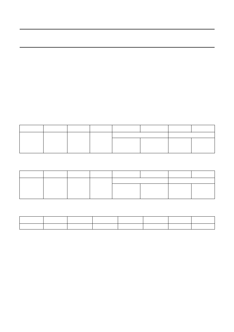
Figure 5 shows the multiplexers with their input and control signals for the DSP processor clock, the microcontroller
clock, the CODEC clock (CLK_3) and the chip input clock frequency. The functional position of the CODEC clock
multiplexer is shown in Fig.4.
handbook, full pagewidth
MGT431
R
S
Q
FF
CLK_3_DRT2
CLK_3_DRT1
CLK_3
CDCCNTRL_CLK
DSP_IDLE
DSP_WAKEUP
DSP_CLK
µ
C_CLK
DSP_CLK_IN
EMG_CLK
EMG_CLK
EMG_CLK
CLK_1
CLK_7
CLK_14
CLK_21
CLK_1
CLK_7
CLK_42
CLK_28
CLK3_CORR
CLK3_OUT
CKCON[2, 3 or 7]
CKCON[4, 5 or 7]
CKCON[6 or 7]
CKCON[0 or 1]
SPCON[0 or 1]
SPCON[2 or 3]
SPCON[4]
˜
4
˜
2
˜
2
˜
5
FS1
FS_event
TIME_event
3
2
1
0
Fig.5 Clock and event rate selection.
2001 Apr 17
16
Philips Semiconductors
Product specification
Digital telephone answering machine chip
PCD6001
9.2.1
S
ELECTION OF SYSTEM CLOCKS
Selection of system clocks involves:
∑
Selection of the crystal input clock in conjunction with
PLL on/off selection (SYMOD register)
∑
Selection of clocks for the DSP, microcontroller and
CODEC, together with microcontroller timing interrupt
rates (CKCON register)
∑
Activation, deactivation of individual clocks or
deactivation of the whole TICB in order to get an
optimum power consumption (SPCON register).
SYMOD, SPCON and CKCON are SFR registers in the
digital section which can be directly accessed by the
microcontroller. Sections 9.2.2 to 9.2.4 summarize the
control registers and settings used for system clock
selection.
The activation of the DSP, and the digital part of both
CODECs is controlled via the SPCON SFR.
The clock rates of the DSP and microcontroller, and the
microcontroller timing interrupt rates are set via the
CKCON SFR.
9.2.2
A
NALOG
S
YSTEM
M
ODE
R
EGISTER
(SYMOD)
Table 3
Analog System Mode Register (SFR address C5H); reset state 00H
9.2.3
S
YSTEM
P
OWER AND
C
LOCK
C
ONFIGURATION
R
EGISTER
(SPCON)
Table 4
System Power and Clock Configuration Register (SFR address 99H); reset state 00H
9.2.4
C
LOCK
C
ONTROL
R
EGISTER
(CKCON)
Table 5
Clock Control Register (SFR address 9AH); reset state 00H
7
6
5
4
3
2
1
0
input clock 1 input clock 0 PLL off/on
V
MIC
off/on
CODEC2; analog
CODEC1; analog
D/A
(loudspeaker)
off/on
A/D
(microphone)
off/on
D/A
(to_line)
off/on
A/D
(from_line)
off/on
7
6
5
4
3
2
1
0
system off
spare
spare
DSP on
CODEC2; digital
CODEC1; digital
D/A
(loudspeaker)
off/on
A/D
(microphone)
off/on
D/A
(to_line)
off/on
A/D
(from_line)
off/on
7
6
5
4
3
2
1
0
EMG mode
RTC mode
DSP clock 1
DSP clock 0
micro clock 1
micro clock 0
FS_event 1
FS_event 0

2001 Apr 17
17
Philips Semiconductors
Product specification
Digital telephone answering machine chip
PCD6001
Table 6 shows the input clock selection in the analog
section of the chip. Note that for 3.456 and 3.58 MHz
crystal input clock, no clock division is done prior to
inputting it to the PLL. After reset the input clock division
rate is by default 1. This means that applications using an
input clock frequency other than 3.456 or 3.580 MHz, will
have to set the proper division rate, after system start-up.
Otherwise proper functionality of the analog blocks is not
guaranteed.
Table 7 shows the microcontroller clock frequencies. In
Emergency mode (bit 7 of CKCON reset), the EMG_CLK
is input directly to the microcontroller. The values of
CKCON bits 2 and 3 are then irrelevant. Note that
Emergency mode operation is only designed for start-up
and POTS mode condition. Peripheral blocks (such as the
CODECs and the IOM block) are not guaranteed to work
when CKCON bit 7 is reset.
Table 6
Input clock selection
Note
1. The PCD6001 timing system is based on the 3.456 MHz (or multiples) input clock frequency. In order to be able to
use the low cost 3.58 MHz crystal or ceramic resonator, a clock frequency correction is needed for some blocks
(RTC, CODEC and IOM). IOM will only operate in Master mode.
Table 7
Microcontroller clock selection
Notes
1. 6 clocks/cycle.
2. If the PLL is switched off when not in Emergency mode, the selected clock would not be available. The micro would
hang up. Before CKCON.7 is set to logic 1, SYMOD.5 must be set to logic 1 to activate the PLL.
CKCON.6
(RTC MODE)
SYMOD.7
(input clock 1)
SYMOD.6
(input clock 0)
INPUT CLOCK
DIVISION RATIO
CHIP INPUT CLOCK
FREQUENCY (MHz)
0
0
0
1
3.456
1
0
0
1
3.580
(1)
0
0
1
2
6.912
0
1
0
4
13.824
CKCON.7
(EMG mode)
CKCON.3
(micro clock 1)
CKCON.2
(micro clock 0)
SYMOD.5
PLL on/off
MICROCONTROLLER
CLOCK FREQUENCY
(1)
0
X
X
X
EMG_CLK
1
X
X
0
do not use
(2)
1
0
0
1
CLK_1
1
0
1
1
CLK_7
1
1
0
1
CLK_14
1
1
1
1
CLK_21

2001 Apr 17
18
Philips Semiconductors
Product specification
Digital telephone answering machine chip
PCD6001
Table 8 shows the DSP clock frequency settings. Setting
the DSP frequency to the correct value according to the
operation mode of the DSP is done by the Application
Programming Interface (API). Please refer to the API
specification for more details.
Table 9 shows CLK_3 selection (CKCON.6/CKCON.7
according to Fig.4). The selection depends on the type of
crystal which is connected (determined by RTC mode
setting according to Table 6). The setting of CKCON [6:7],
thus determines the selection of the CLK_3 source (see
Table 2 and Fig.4). If CKCON.7 = 0 to denote Emergency
mode - CLK_3 will be derived from the EMG_CLK, as
shown in the following tables.
The TICB provides two periodic outputs to the
microcontroller: FS_event and TIME_event. FS_event is
programmable to 4 different rates. Both outputs are
derived from and therefore synchronized to FS1. The
outputs are connected to an interrupt input of the
microcontroller and called `Time_event interrupt' and
`FS_event interrupt' respectively. The selection of the
FS_event interrupt rate is done via the CKCON SFR, see
Section 9.2.4. Figure 8 shows the generation of these
interrupts. Table 10 shows the selection of the FS_event
rate. The FS1 clock is provided by the CDCCNTRL block
shown in Fig.4.
Table 8
DSP clock selection
Table 9
CODEC clock selection
Note
1. A phase corrected CLK_3 clock is not available in Emergency mode (CKCON.7 = 0). For a CLK_3 phase correction
(CKCON.6 = 1), CLK_21 must be available.
Table 10 FS_event rate selection
CKCON.7
(EMG mode)
CKCON.5
(DSP clock 1)
CKCON.4
(DSP clock 0)
SYMOD.5
(PLL on/off)
DSP CLOCK
FREQUENCY
0
X
X
X
EMG_CLK
1
X
X
0
no clock active
1
0
0
1
CLK_1
1
0
1
1
CLK_7
1
1
0
1
CLK_42
1
1
1
1
CLK_28
CKCON.7
(EMG mode)
CKCON.6
(RTC mode)
CLK_3 SOURCE
0
X
EMG_CLK
(1)
1
1
CLK3_CORR
1
0
CLK3_OUT
CKCON.1
(FS_event 1)
CKCON.0
(FS_event 0)
FS_event INTERRUPT RATE
0
0
FS1/16
500 Hz
2 ms
0
1
FS1/8
1 kHz
1 ms
1
0
FS1/4
2 kHz
500
µ
s
1
1
FS1
8 kHz
125
µ
s

2001 Apr 17
19
Philips Semiconductors
Product specification
Digital telephone answering machine chip
PCD6001
9.3
Real-Time Clock generation
The Real-Time Clock (RTC) divider provides a 1 minute
timing signal which is available as an interrupt to the
microcontroller. The RTC_CLK input clock is always
active, whether the PLL is active or not. Thus the complete
chip can be set into Power-down mode (but not System-off
mode), where the microcontroller can be woken up by the
RTC to maintain the values for date and time. The
RTC_CLK is directly derived from the EMG_CLK input
clock signal.
Figure 6 shows the RTC clock generation. To divide a
3.456 or a 3.580 MHz clock into a 1 minute RTC signal a
28 bit counter is required to count 60
◊
3.456
◊
10
6
clock
periods. To determine the number of most significant bits
of this counter required for an accurate RTC, the maximum
allowed time deviation per month and the crystal accuracy
need to be taken into account. The LSB of the 28 counter
has an accuracy of 1/(60
◊
3.456
◊
10
6
) = 0.005
parts-per-million (ppm). Since a normal crystal accuracy is
about 10 ppm it is tolerable to have only the 17 MSB of the
counter available (10/0.005 = 2000, which implies that the
11 LSB can be disregarded), as shown in Fig.6.
If one month is set to 30
◊
24
◊
60
◊
60 = 2.6
◊
106
seconds, 10 ppm deviation equals 26 seconds per month
or about 5 minutes per year.
Since there are 2 possible RTC_CLK values, 3.580 and
3.456 MHz, there are 2 comparators selectable for the
RTC; COMP_3.580 and COMP_3.456. The nominal value
of these comparators are (11 LSB are set to logic 0):
COMP_3.580: CCD2800H (RTCON = A5H)
COMP_3.456: C5C1000H (RTCON = 82H).
In Section 9.2 the conditions for the RTC_MODE signal
are described.To allow connection of various crystals or
ceramic resonators, as well as to provide adjustment of the
RTC clock according to the crystal tolerance, 8 of the 17
most significant bits of the comparators are programmable
via the SFR register RTCON. The binary values of the
comparators are then as shown in Table 11.
Since the accuracy of Q11 is 10 ppm, with the adjustment
of the RTC via RTCON an accuracy of
±
5 ppm can be
achieved. For an RTC pulse every 1 minute the outer limits
of the crystal frequency inputs which can be connected
are:
COMP_3.580 (max): CCFF800H
3.582600 MHz
COMP_3.580 (min): CC80000H
3.573897 MHz.
COMP_3.456 (max): C5FF800H
3.460267 MHz
COMP_3.456 (min): C580000H
3.451563 MHz.
The default value of RTCON for an input frequency
3.58 MHz is A5H and for an input frequency of 3.456 MHz
is 82H.
Table 11 Comparator contents
Q27
Q18
Q11
COMP_3.580
1
1
0
0
1
1
0
0
1
x
x
x
x
x
x
x
x
COMP_3.456
1
1
0
0
0
1
0
1
1
x
x
x
x
x
x
x
x
bit 7
RTCON
bit 0
handbook, full pagewidth
MGM770
17
17
17
Q11 to Q27
EMG_CLK
Q10
Q0
28 BIT
RIPPLE
COMP_3.456
COMP_3.580
0
1
RTC_MODE
0: RTC_CLK = 3.456 MHz
1: RTC_CLK = 3.580 MHz
synch_reset
RTC_event
Fig.6 Real-Time Clock (RTC) generation.

2001 Apr 17
20
Philips Semiconductors
Product specification
Digital telephone answering machine chip
PCD6001
10 THE MICROCONTROLLER
The embedded MS80C51 microcontroller controls the
Digital Telephone Answering Machine (DTAM) chip by
means of Special Function Registers (SFRs). SFRs are
defined for the blocks MCB, TICB, PCON, DSP, I
2
C-bus,
ports P1, P3 and P4, MA, MSK and ANA (the analog
blocks). All of these (except SFR PCON) are shown in the
block diagram in Fig.1. The architecture of the
microcontroller itself and the interface to these blocks are
described in this chapter.
10.1
Microcontroller architecture
The microcontroller architecture and its environment is
shown in Fig.7.
The microcontroller has some application-specific
peripherals such as the I
2
C-bus, Watchdog Timer (WD),
P1, P3, P4, MCB, External Interface with MA port, SFRs of
the DSP block, the TICB and the ANA block. Most of these
functions and SFRs are located in the Application Specific
Function block (ASF), see Fig.7.
The 80C51 core contains the 80C51 standard functions
such as Timer 0 and Timer 1, power-down/idle states and
a 15 vector dual-level interrupt controller INT15L2.
Furthermore, the microcontroller contains the Metalink
enhanced hooks protocol which enables Metalink
emulation via ALE, PSEN, EA, P0 and P2. The external
program memory access is done via the standard Ports P0
and P2. Connection of external flash memory is done via
the P4, P0 and P2 I/O pads. The microcontroller Clock
Driver (CD) has no clock divider, which means that the
microcontroller operates on 6 microcontroller_CLK clocks
per machine cycle.
The 80C51 has a few basic modes of operation: Reset,
Normal, Metalink, Test (various) Idle and Power-down.
Entering the Metalink mode can be done via inputs ALE
and EA during a reset.
The Idle mode can be entered by setting the IDL bit in the
PCON register. Leaving the Idle mode can be done via a
master reset (RSTIN), any external interrupt, a
DSP_event, TIME_event or RTC_event, Timer 0 and
Timer 1, I
2
C-bus interrupt, MSK_event or FS_event; if
these interrupts are enabled.
The Power-down mode can be entered by setting the
PD bit in PCON. The power-down logic of the
microcontroller will turn all microcontroller clocks off.
The TIME_event, DSP_event, RTC_event and
EX2 to EX6 are mixed with EX0 (see Fig.10) and therefore
make use of the standard wake-up circuitry of the 80C51.
These interrupts should be active for more than 6 clocks
(read, modify, write of IRQ1 takes 1 instruction) to
guarantee the interrupt for the microcontroller.
Setting the PD bit of PCON after setting the system-off bit
of SPCON, will trigger the analog section to turn off the
oscillator and therefore the whole chip. In order to keep
static supply currents minimal, it is advised to switch off the
digital-to-analog part of the CODECs before going in this
system-off mode. Wake-up from system-off can be done
via a RSTIN or an external interrupt EX0 to EX6 (if the EX0
interrupt is enabled) or EX1 (if the EX1 interrupt is
enabled). A wake-up from system-off will always reset the
PCD6001. The EX interrupt condition should last more
than 4096 + 64 + 4 clocks to be sure that the interrupt is
handled when entering the normal mode. If the interrupt is
shorter the microcontroller will only enter the normal mode
after the reset is gone.
10.2
Memory mapping
The memory map of the 80C51 is shown in Fig.8.
In addition to all the SFRs, the microcontroller has
128 bytes of directly addressable (DATA) memory,
128 bytes of indirectly addressable (IDATA) memory and
512 bytes of AUX RAM, the on-chip `MOVX' addressable
(XDATA) memory. On-chip XDATA memory access can
be disabled by setting the ARD bit in PCON to logic 1. The
internal 32-kbyte ROM of microcontroller program (CODE)
memory can be accessed when EA is set to logic 1.
Via Ports P0, MA, P2 and P4 it is possible to access up to
512 kbytes of external speech data memory stored in a
parallel flash memory. A CAD flash memory can also be
mapped in this area. A serial (SPI or Microwire compatible)
flash memory can be connected to P4 which is controlled
by the MCB. Up to 64 kbytes of program (CODE) memory
can be connected to the P0, P2 and PSEN pads. This can
be any external program memory (like the MON51 target
debug ROM) if EA is logic 0.
When the EAM SFR bit (P4CFG.5) is logic 0 (default after
reset), the XRAM-mapped control registers can only be
accessed if P4.3 is logic 1. Otherwise, XRAM addressing
is independent of the value of the P4.3 SFR bit.

2001 Apr 17
21
Philips Semiconductors
Product specification
Digital telephone answering machine chip
PCD6001
handbook, full pagewidth
MGT432
IRQ1/IX1
GROUP
IF
MSK
TICB
ANA
ANALOG
FUNCTIONS
DSP
I/O PADS
P1, P3
RD,WR
FLASH
I
2
C-BUS
FLASH
CAD
FLASH
PARALLEL
FLASH
MICROWIRE/
SPI
EXTERNAL
64-kbyte
SRAM
I/O PADS
P4
DSP
CD
MSEL
PORT1
WD
WDRST
PORT3
MODE
CONTROL
RAMIF
CPU
XMEMU
PORT4
I PAD
RST_IN
I PAD
RST_ANA
O PAD
MRST
O PAD
DIS_XTAL
I
2
C-BUS
I
2
C-bus_int
ARD
PCON.2
to
PCON.7
MCB
I/O PADS
P0, P2
PSEN
EA
ALE
SF
GROUP INT.
TIMER 0
TIMER 1
PCON.0
to
PCON.1
INT15L2
SRAM
MAIN/AUX
RAM
256/512
BYTES
APPLICATION
SPECIFIC
FUNCTIONS
EX0 to EX6
DSP_req
MSK_INT
ROMIF
INTERNAL
32 KBYTE
ROM
µ
CMS 80C51 CORE
µ
C_CLK
MRST
osc_off
pad_ale
pad_ea_n
TICBIF
SPCON[7]
DSP_event
TIME_event
RTC_event
FS_event
TICB
DRAM
ARAM
Fig.7 Microcontroller (MS 80C51) architecture and environment.

2001 Apr 17
22
Philips Semiconductors
Product specification
Digital telephone answering machine chip
PCD6001
handbook, full pagewidth
MGT433
External program
memory
External data
memory
Internal XDATA
memory
Internal ROM
AUX RAM
ConfReg
MA
P2
EA = 1
XDATA
IDATA
Main RAM
SFR
DATA
128
255
48
32
0
BIT
ADDRESSABLE
SPACE
REGISTER
BANKS 0 TO 3
P4.3 = X
ARD = X
P4.3 = 0
ARD = 1
XDATA
ARD = 0
P4.3 = X
ARD = 1
CODE
CODE
64K
32K
518
515
512
EA = 1
XDATA-mapped registers
P4.3 = 1, EAM = 0, ARD = X
or ARD = 0, EAM = 1, EA = 1
Fig.8 Microcontroller memory map.
2001 Apr 17
23
Philips Semiconductors
Product specification
Digital telephone answering machine chip
PCD6001
10.3
SFR mapping
The SFR mapping for the microcontroller is shown in Table 12. All SFRs and their reset states are described in Table 13.
Table 12 SFR mapping
Notes
1. SFRs in this column are both bit and byte-addressable.
2. Complies to 80C51 family architecture specification.
3. These registers are read only (all other SFRs are read/write).
4. Reserved register, used for testing purposes. Writing of reserved or undocumented bits might lead to unexpected
behaviour of the device (see Section 10.8).
SFR
ADDRESS
(HEX)
SPECIAL FUNCTION REGISTERS 8 BITS EACH
ADDRESSABLE
(1)
ONLY BYTE ADDRESSABLE
F8 to FF
IP1
(2)
-
-
-
-
-
-
WDT
(2)
F0 to F7
B
(2)
-
-
-
-
-
-
WDTKEY
E8 to EF
IEN1
(2)
IX1
-
-
-
-
-
-
E0 to E7
ACC
(2)
-
-
-
-
-
-
-
D8 to DF
S1CON
(2)
S1STA
(2)(3)
S1DAT
(2)
S1ADR
(2)
-
-
-
-
D0 to D7
PSW
(2)
-
-
-
-
-
-
-
C8 to CF
MCON
MBUF
MSTAT
-
-
-
-
-
C0 to C7
IRQ1
INTC
GPADR
(3)
GPADC
GPDAR
SYMOD
-
DTCON
B8 to BF
IP0
(2)
XWUD
V
REFR
CDVC1
CDVC2
CDTR1
(4)
-
TCTRL
(4)
B0 to B7
P3
(2)
-
-
-
-
PMTR1
(4)
PMTR2
(4)
CDTR2
(4)
A8 to AF
IEN0
(2)
MCSC
MCSD
ALTP
-
-
-
-
A0 to A7
-
-
DTM0
(3)
DTM1
(3)
DTM2
(3)
MTD0
MTD1
MTD2
98 to 9F
P4
SPCON
CKCON
RTCON
-
CDTR1
(4)
-
P4CFG
90 to 97
P1
(2)
-
-
-
-
-
-
-
88 to 8F
TCON
(2)
TMOD
(2)
TL0
(2)
TL1
(2)
TH0
(2)
TH1
(2)
-
-
80 to 87
-
SP
(2)
DPL
(2)
DPH
(2)
-
-
-
PCON

2001 Apr 17
24
Philips Semiconductors
Product specification
Digital telephone answering machine chip
PCD6001
Table 13 Microcontroller register list
NAME
ADDRESS (HEX)
DESCRIPTION
RESET STATE
(1)
ACC
E0
accumulator
0000 0000
ALTP
AB
LE and GPC control
X
000 0000
A
-
accumulator
0000 0000
B
F0
B register for multiply, divide or scratch
0000 0000
CKCON
9A
Clock Control Register
0000 0000
CDVC1
BB
CODEC digital volume control for CODEC1
00
XX
0
XXX
CDVC2
BC
CODEC digital volume control for CODEC2
00
XX
0
XXX
CDTR1
BD
CODEC Test Register 1; see note 1
00
XX
0
XXX
CDTR2
B7
CODEC Test Register 2; see note 2
00
XX
0
XXX
DTCON
C7
line selection and alternative gain control register
XX
00
X
00
X
DPL
82
data pointer low
0000 0000
DPH
83
data pointer high
0000 0000
DTM0
A2
DSP to Microcontroller Communication Register 0 (read only)
0000 0000
DTM1
A3
DSP to Microcontroller Communication Register 1 (read only)
0000 0000
DTM2
A4
DSP to Microcontroller Communication Register 2 (read only)
0000 0000
GPADC
C3
automatic analog-to-digital conversion, channel select, request
confirm
XXXX X
000
GPADR
C2
digital value of analog input (read only)
0000 0000
GPDAR
C4
digital value of analog output
1000 0000
IEN0
A8
Interrupt Enable Register 0
0000 0000
IEN1
E8
Interrupt Enable Register 1
0000 0000
INTC
C1
Interrupt Control Register
XXXX XX
00
IP0
B8
Interrupt Priority Register 0
X
000 0000
IP1
F8
Interrupt Priority Register 1
0000 0000
IRQ1
C0
Interrupt Request Flag Register
0000 0000
IX1
E9
Interrupt Polarity Register
XXX
0 0000
MCSD
AA
Memory Control Serial Data Register
0000 0000
MCSC
A9
Memory Control Serial Command Register
XXXX
0000
MTD0
A5
microcontroller to DSP communication register 0
0000 0000
MTD1
A6
microcontroller to DSP communication register 1
0000 0000
MTD2
A7
microcontroller to DSP communication register 2
0000 0000
MCON
C8
MSK Control Register
0000 0000
MBUF
C9
MSK Data Buffer Register
XXXX XXXX
MSTAT
CA
MSK Status Register
0X00 0000
P1
90
general purpose digital I/O
1111 1111
P3
B0
general purpose digital I/O
1111 1111
P4
98
P4 can be used to control flash memory
XX
01 1110
P4CFG
9F
P4 configuration and addressing mode register
0000 0000
PCON
87
Power and Interrupt Control Register
X
000 0000
PMTR1
B5
Power Management Test Register 1; see note 2
0000 0000

2001 Apr 17
25
Philips Semiconductors
Product specification
Digital telephone answering machine chip
PCD6001
Notes
1. All SFR bits with reset state `X' are either `spare' (i.e. have a memory bit in this position with reset state `0') or `-' (i.e.
do not have a physical memory bit in this position). All `spare' bits can be addressed and used as additional general
purpose bits. All bits marked `-' cannot be addressed by the user. To see which bits are `spare' or `-' refer to the
respective SFR layouts.
2. Reserved registers, used for testing purposes. Writing of undocumented or reserved bits might lead to unexpected
behaviour of the device (see Section 10.8).
PMTR2
B6
Power Management Test Register 2; see note 2
0000 0000
PSW
D0
Program Status Word
0000 0000
RTCON
9B
Real-Time Clock control
0000 0000
S1CON
D8
I
2
C-bus Serial Control Register
0000 0000
S1ADR
DB
I
2
C-bus own slave address register
0000 0000
S1DAT
DA
I
2
C-bus Data Shift Register
0000 0000
S1STA
D9
I
2
C-bus Status Register (read only)
1111 1000
SYMOD
C5
analog system mode control
0000 0000
SPCON
99
system power and clock configuration
0
XX
0 0000
SP
81
Stack Pointer
0000 0111
TCON
88
Timer/counter Control Register
0000 0000
TMOD
89
Timer/counter Mode Control Register
0000 0000
TL0
90
Timer Low Register 0
0000 0000
TL1
91
Timer Low Register 1
0000 0000
TH0
92
Timer High Register 0
0000 0000
TH1
93
Timer High Register 1
0000 0000
VREFR
BA
Voltage Reference Register
1010 0000
WDT
FF
Watchdog Timer
0000 0000
WDTKEY
F7
Watchdog Key Register
0000 0000
XWUD
B9
external wake-up disable
0000 0000
NAME
ADDRESS (HEX)
DESCRIPTION
RESET STATE
(1)

2001 Apr 17
26
Philips Semiconductors
Product specification
Digital telephone answering machine chip
PCD6001
10.4
Microcontroller interrupts
The microcontroller has 15 interrupt sources, shown
below, which can be programmed to have a low or high
priority. If enabled these interrupts sources result in jump
to the addresses shown in Table 14.
∑
EX2 to EX6 asynchronous external interrupts via
P1.0 to P1.4
∑
EX0 and EX1 asynchronous external interrupts via
P3.2 (INT0N) and P3.3 (INT1N)
∑
DSP_event
∑
FS_event
∑
TIME_event
∑
I
2
C-bus interrupt
∑
RTC_event
∑
Timer 0 and Timer 1 interrupt
∑
MSK interrupt.
The external interrupt configuration of P1 is shown in
Fig.9. Pins P1.5, P1.6 and P1.7 cannot be used as
external interrupts. The IX1 SFR determines the polarity of
the external interrupt sources of P1. Clearing the `global
enable' bit in IEN0 disables all interrupt sources. Using
IEN0 (and IEN1) each individual external interrupt can be
enabled or disabled.
The IRQ1 SFR stores all external interrupts. So if an
external interrupt with a low priority is detected during
execution of another (high or low priority) interrupt it will be
handled just after the return of this interrupt.
The interrupt service routine for an external interrupt must
clear the right IRQ1 flag to indicate that it has serviced the
interrupt request. Notice that during the interrupt routine
this flag can be set again immediately after clearing the
IRQ1 flag if the interrupt source is (still) HIGH.
The complete interrupt system is shown in Fig.10. All
15 interrupts are allocated and can be given a low or high
priority according to the setting of IP0 and IP1.
Each interrupt source can be individually enabled by
means of IEN0 and IEN1.
The IRQ1 and IX.7 registers are clocked (a clock which is
active during Idle) and can be set by P1.0 to P1.4, the
TIME_event, the DSP_event, the FS_event and the
RTC_event. These flags can only be cleared by software.
Only TCON.1, TCON.3, TCON.5 and TCON.7 flags are
cleared by the interrupt controller hardware. All other flags
must be cleared by software.
The polling of a potential interrupt goes from a high priority
to a low priority interrupt. Within a high (or low) priority
interrupt level the EX0 (if set to high priority) will be polled
first followed by the next high priority interrupt.
The interrupt SFRs IP0, IP1, IEN0, IEN1, IRQ1 and IX1 are
defined in Sections 10.4.1 to 10.4.6. A flag set to logic 1 in
IP0 or IP1 (Tables 15 and 16) causes the corresponding
interrupt to have high priority.

2001 Apr 17
27
Philips Semiconductors
Product specification
Digital telephone answering machine chip
PCD6001
Table 14 Allocation of interrupt sources
Notes
1. For some C-compilers `1' has to be added to this number.
2. The interrupt controller supports up to 15 interrupt sources, each with a 2-level (high or low) priority. High priority
interrupt is always serviced before a low priority interrupt, but within the high and low levels, interrupts are serviced
in the order shown in this column.
VECTOR
SOURCE
NUMBER
(1)
PRIORITY
(2)
DESCRIPTION
IENx/IPx
0003
EX0
0
1
external interrupt 0
IEN0.0/IP0.0
000B
T0
1
4
Timer 0 interrupt
IEN0.1/IP0.1
0013
EX1
2
7
external interrupt 1
IEN0.2/IP0.2
001B
T1
3
10
Timer 1 interrupt
IEN0.3/IP0.3
0023
MSK_event
4
13
MSK RI or TI interrupt
IEN0.4/IP0.4
002B
TIME_event
5
2
TIME interrupt
IEN0.5/IP0.5
0033
FS_event
6
5
FS interrupt
IEN0.6/IP0.6
003B
EX2
7
8
external interrupt 2
IEN1.0/IP1.0
0043
EX3
8
11
external interrupt 3
IEN1.1/IP1.1
004B
EX4
9
14
external interrupt 4
IEN1.2/IP1.2
0053
EX5
10
3
external interrupt 5
IEN1.3/IP1.3
005B
EX6
11
6
external interrupt 6
IEN1.4/IP1.4
0063
I
2
C-bus
12
9
I
2
C-bus interrupt
IEN1.5/IP1.5
006B
DSP_event
13
12
DSP interrupt
IEN1.6/IP1.6
0073
RTC_event
14
15
RTC interrupt
IEN1.7/IP1.7
handbook, full pagewidth
MGM773
P1.7
P1.6
P1.5
P1.4
P1.3
P1.2
P1.1
P1.0
IX1
IEN1
RTC
FS
TIME
EX6
EX5
EX4
EX3
EX2
IRQ1
RTC_event
DSP_event
TIME_event
Fig.9 Port 1 external interrupt configuration.
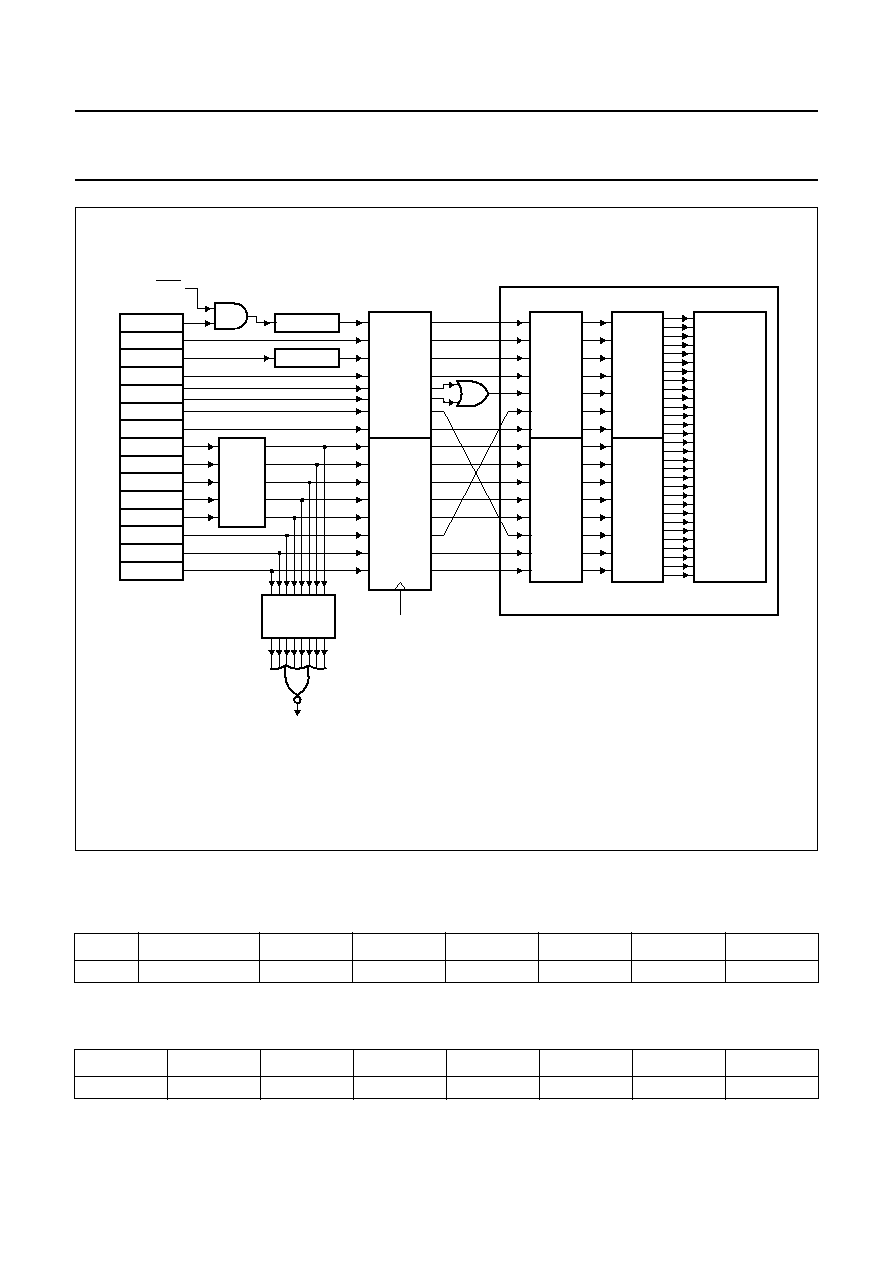
2001 Apr 17
28
Philips Semiconductors
Product specification
Digital telephone answering machine chip
PCD6001
10.4.1
I
NTERRUPT
P
RIORITY
R
EGISTER
0 (IP0)
Table 15 Interrupt Priority Register 0 (SFR address B8H); reset state 00H
10.4.2
Interrupt Priority Register 1 (IP1)
Table 16 Interrupt Priority Register 1 (SFR address F8H); reset state 00H
7
6
5
4
3
2
1
0
-
priority FS_event
priority TIME
priority MSK
priority T1
priority EX1
priority T0
priority EX0
7
6
5
4
3
2
1
0
priority RTC
priority DSP
priority I
2
C
priority EX6
priority EX5
priority EX4
priority EX3
priority EX2
handbook, full pagewidth
MGM774
TIME_event
FS_event
DSP_event
RTC_event
EX6
EX5
EX4
EX3
EX2
IX.4
IX.3
IX.2
IX.1
IX.0
MSK
T1
EX1
T0
EX0
I
2
C-BUS
TCON.0
TCON.1
IEN0.0
IEN0.1
IEN0.2
IEN0.3
IEN0.4
IEN0.5
IEN0.6
IEN1.0
IEN1.1
IEN1.2
IEN1.3
IEN1.4
IEN1.5
IEN1.6
IEN1.7
TCON.5
TCON.3
TCON.7
MSTAT.0
MSTAT.1
S1CON.3
INTC.0
IRQ1.0
IRQ1.1
IRQ1.2
IRQ1.3
IRQ1.4
IRQ1.5
IRQ1.6
IRQ1.7
clocks
EXP1N
XWUD.0
to
XWUD.7
XWUD
EDGE/LEVEL
SOURCE
FLAGS
ENABLE
TCON.2
IP0.0
IP0.1
IP0.2
IP0.3
IP0.4
IP0.5
IP0.6
IP1.0
IP1.1
IP1.2
IP1.3
IP1.4
IP1.5
IP1.6
IP1.7
PRIORITY
INTERRUPT
SCANNING
INTERRUPT CONTROLLER
EXP1N
+
XWU
POLARITY
Fig.10 PCD6001/80C51 interrupt system.
2001 Apr 17
29
Philips Semiconductors
Product specification
Digital telephone answering machine chip
PCD6001
10.4.3
I
NTERRUPT
E
NABLE
R
EGISTER
0 (IEN0)
Table 17 Interrupt Enable Register 0 (SFR address A8H); reset state 00H
10.4.4
I
NTERRUPT
E
NABLE
R
EGISTER
1 (IEN1)
Table 18 Interrupt Enable Register 1 (SFR address E8H); reset state 00H
10.4.5
I
NTERRUPT
R
EQUEST
F
LAG
R
EGISTER
(IRQ1)
Table 19 Interrupt Request Flag Register 1 (SFR address C0H); reset state 00H; note 1
Note
1. The flags of IRQ1 will be set to logic 1 by hardware if the interrupt occurs. They must be cleared by software in the
interrupt service routine.
10.4.6
I
NTERRUPT
P
OLARITY
R
EGISTER
(IX1)
Table 20 Interrupt Polarity Register (SFR address E9H); reset state 00H; note 1
Note
1. A polarity bit set to logic 1 in IX1 will cause the external interrupt to be active HIGH.
10.4.7
I
NTERRUPT
C
ONTROL
R
EGISTER
(INTC)
Table 21 Interrupt Control Register (SFR address C1H); reset state 00H
10.4.8
E
XTERNAL
W
AKE
-
UP
D
ISABLE
R
EGISTER
(XWUD)
Table 22 External Wake-up Disable Register (SFR address B9H); reset state 00H
7
6
5
4
3
2
1
0
global
enable
enable
FS_event
enable TIME
enable
MSK_event
enable T1
enable EX1
enable T0
enable EX0
7
6
5
4
3
2
1
0
enable RTC
enable DSP
enable I
2
C
enable EX6
enable EX5
enable EX4
enable EX3
enable EX2
7
6
5
4
3
2
1
0
RTC flag
DSP flag
TIME flag
EX6 flag
EX5 flag
EX4 flag
EX3 flag
EX2 flag
7
6
5
4
3
2
1
0
spare
spare
spare
polarity EX6
polarity EX5
polarity EX4
polarity EX3
polarity EX2
7
6
5
4
3
2
1
0
spare
spare
spare
spare
spare
spare
extended
wake-up;
XWU
FS flag
7
6
5
4
3
2
1
0
RTC XWU
disable
DSP XWU
disable
TIME XWU
disable
EX6 XWU
disable
EX5 XWU
disable
EX4 XWU
disable
EX3 XWU
disable
EX2 XWU
disable

2001 Apr 17
30
Philips Semiconductors
Product specification
Digital telephone answering machine chip
PCD6001
10.5
Interface to DSP
The DSP to Microcontroller Interface (DMI) can be used for
the following purposes:
∑
Transferring compressed speech data from
microcontroller to DSP
∑
Transferring compressed speech data from DSP to
microcontroller
∑
Transferring DSP parameters (DSP mode, tone
frequency etc.) from microcontroller (API) to the DSP
∑
Transferring DSP events (Caller ID, Ring Detect, VOX,
Call Progress etc.) to the microcontroller.
The microcontroller and the DSP can communicate by
means of 6 SFRs (MTD0, MTD1 and MTD2 and DTM0,
DTM1 and DTM2) and 4 DSP I/O registers (DTMC,
DTMD, MTDC and MTDD), see Fig.11. The DTMC and
MTDC registers are used for communication and control
and the DTMD and MTDD registers for transferring data.
The Micro Transmit (MT), DR (DSP receive) and DT (DSP
Transmit), Micro Receive (MR) ensure that either the old
data is read or new data is read although the DSP and
microcontroller operate on different clocks. This can be
achieved by means of simple handshake circuitry in either
direction. The DR state machine ensures that the DSP will
never read new MTDC control data and old MTDD speech
data. In order to guarantee proper transitions of the
DR state machine the DSP always has to read the DTMC
first and afterwards the DTMD IO register.
The TICB generates the DSP_event interrupt when it
receives a dsp_uc_req signal. The dsp_uc_req cannot be
generated by the microcontroller because the dsp_event
interrupt must be able to wake-up the microcontroller from
Power-down.
MTD0/1/2 are written by the microcontroller. After each
write to MTD0 the contents of MTD0/1/2 are transferred to
the 16-bit register MTDD and the 8-bit register MTDC (the
MSB is set to 00H), which can be read by the DSP via the
DSP I/O bus. In this way the DSP always receives a valid
control byte and a valid 16-bit data word. If MTD0 is written
while the DSP is turned off the MTD0 value will be
transferred to the MTDC IO-register as soon as the DSP is
turned on.
The MTDC and MTDD registers are continuously and
immediately read by the DSP after every FS1 interrupt.
The microcontroller can write a new word to MTD0/1/2 but
has to wait for at least 125
µ
s to be sure that the DSP has
read the previous value.
DTM0/1/2 are read by the microcontroller as SFRs. The
contents of the DTMD and DTMC registers are transferred
to the DTM0/1/2 SFRs when the DSP writes the DTMC
register. At this time an interrupt signal called DSP_event
is generated to the microcontroller, which triggers the
microcontroller to read the DTM0/1/2 SFRs. In this way
DSP events and speech data can be transferred easily to
the microcontroller. The DSP will transfer a maximum of
3 bytes, one command byte and two data bytes, for
example; every 125
µ
s to the microcontroller. Thus one
write to DTMC takes place every 125
µ
s.
Similarly, the microcontroller can transfer a maximum of
3 bytes every 125
µ
s to the DSP. Thus one write to MTD0
takes place every 125
µ
s. The default rate for the
FS_event interrupt will be FS1/8 resulting in a data transfer
rate of 10 words every 10 ms which equals 16 kbits/s.
In case a higher rate is needed the FS_event interrupt rate
can be switched to FS1/4.
10.6
Interface to Real-Time Clock (RTC)
When the RTC_event interrupt is enabled in IEN1 and the
`global enable' bit in IEN0 is set and the PCD6001 is not in
Emergency mode (CKCON.7 = 1), the microcontroller will
get an RTC_event interrupt every 1 minute. The RTC
interrupt service routine must clear the RTC flag. The
RTC_event interrupt will also wake-up the microcontroller
when it is in the Power-down or in the Idle state. Under
power saving conditions this will allow the user to switch off
the microcontroller and still maintain an accurate real time
clock.

2001 Apr 17
31
Philips Semiconductors
Product specification
Digital telephone answering machine chip
PCD6001
handbook, full pagewidth
MGM775
LSB
DTMC
LSB
MTDC
DR
MTDC/D write
rd_MTDD
rd_MTDC
MT
DT
DTMC write
µ
c_dsp_ack
dsp_
µ
c_req
µ
c_dsp_req
dsp_
µ
c_ack
dsp_
µ
c_req
dsp_clk
µ
C_CLK
DSP_event
DTM0,
DTM1 or DTM2
FS1
interrupt
FS_event
MR
LSB
DTMD
MSB
MTD0 write
LSB
MTDD
MSB
DTM0
MTD0
DTM1
DTM2
MTD1
MTD2
RD16010
MICRO-
CONTROLLER
80C51
DSP
IO
TICB
µ
CMS 80C51
SFR
Fig.11 DSP to Microcontroller Interface (DMI).

2001 Apr 17
32
Philips Semiconductors
Product specification
Digital telephone answering machine chip
PCD6001
10.7
Interface to the Memory Control Block (MCB)
The MCB is a 3-wire serial interface designed to interface
with a versatile range of serial flash memories (both
Microwire and SPI mode 0/3 compatible slave devices) in
parallel with program OTP/external ROM and even
external data SRAM.
The 3-wire serial interface consists of a serial data output
(FSO) serial data input (FSI) and a serial clock signal
(FSK). FSK, FSO and FSI are alternative functions of the
general purpose I/O pins P4.1, P4.2 and P4.4. The serial
interface is controlled via the MCSC and MCSD SFRs. The
FSK and FSO outputs are both open-drain and must be
pulled to 3 V with external resistors R
FSK
and R
FSO
. The
recommended value for both resistors at high FSK speeds
(>1 MHz) is 1 k
. The MCSC SFR is defined in
Section 10.7.1.
Turning the MCB on by setting bit MCSC.3, will switch the
FSK and FSO pins to logic 0. A write to MCSD will
generate the appropriate FSK/FSO signal. A read from
MCSD will only generate 8 FSK pulses and will shift-in the
next byte. The shifting and the FSK/FSO signal can be
suppressed by setting bit 2 of MCSC. This can be used for
reading the last byte out of the serial flash memory during
a read sequence. The FSK shift off operation however is
not necessary if the MCB is already turned off when
reading the MCSD SFR for the last time.
If a serial flash memory is chosen the FSK master clock
rate can be selected with bits 0 and 1, as shown in
Table 24. The MCB is always master, which means that
the FSK clock is always generated by the PCD6001.
Depending on the FSK clock rate, the shifting can continue
for 8
◊
32 microcontroller_CLK periods. During this period,
the microcontroller should not be put in a power saving
mode (Idle, Power-down and System-off), otherwise the
shifting will stop.
Data coming from or going to the serial flash memory can
be accessed by means of the MCSD SFR. This is simply
an 8-bit serial shift register. The first FSO and FSI bits are
always the most significant bits of MCSD. The first read of
the MCSD SFR will only serially load the MCSD SFR with
valid data. Therefore, the first read operation must always
be followed with another read operation which reads the
actual received data out of the MCSD SFR.
The serial shifting of bits into and out of MCSD is done at
the same moment: 1 microcontroller clock before the
falling edge of FSK (t
SF
). When the FSK speed is
programmed at the highest speed (microcontroller_CLK/4)
this shifting will be done in the middle of the FSK HIGH
level time. The most time-critical situation is when FSK is
only 2 clocks wide and has a frequency of 3.5 MHz
(14 MHz/4). In this case make sure that t
r(FSK)
, which can
be controlled by the value of R
FSK
, is greater than the hold
time requirement of the slave device.
Figure 12 shows how a Microwire compatible device can
be accessed with an FSK speed of microcontroller_CLK/4.
A SPI mode 0/3 device requires an additional FSK clock
falling edge to trigger the slave device to generate valid
data on the FSI line. The SPI mode 3 can be achieved by
starting with FSK high when the device is turned on (turn
MCB on after asserting the chip enable of the slave device)
and by ending with FSK. The SPI mode 0 can be achieved
by generating an additional FSK pulse (by turning the MCB
off and on again, see Fig.12) between the last write to
MCSD and the first read of MCSD.
A variety of serial flash memory driver software packages
is included in the API software for the microcontroller that
is provided with the chip.
An application note is available to help implementation of
the software for the SPI.
10.7.1
M
EMORY
C
ONTROL
S
ERIAL
C
OMMAND
R
EGISTER
(MCSC)
Table 23 Memory Control Serial Command Register (SFR address A9H)
Table 24 Selection of FSK clock rate
7
6
5
4
3
2
1
0
spare
spare
spare
spare
MCB on
shift off
FSK rate 1
FSK rate 0
MCSC.1
MCSC.0
FSK CLOCK RATE
0
0
microcontroller_CLK/4
0
1
microcontroller_CLK/8
1
0
microcontroller_CLK/16
1
1
microcontroller_CLK/32

2001 Apr 17
33
Philips Semiconductors
Product specification
Digital telephone answering machine chip
PCD6001
Table 25 MCB timing
Notes
1. N depends on the chosen FSK clock rate and can be 4, 8, 16 and 32.
2. The rise time of FSK and FSO depends on the externally connected pull-up resistor and the capacitive load.
SYMBOL
PARAMETER
VALUE
T
FSK
FSK period
N
◊
t
micro_clock
; note 1
t
su(FSO)
FSO setup time with respect to the rising edge of FSK
(N/2 + 1)
◊
t
micro_clock
-
t
r(FSO)
t
h(FSO)
FSO hold time with respect to the rising edge of FSK
(N/2
-
1)
◊
t
micro_clock
-
t
r(FSK)
t
r(FSK)
FSK rise time
note 2
t
r(FSO)
FSO rise time
note 2
t
su(FSI)
FSI setup time with respect to the internal shift clock
(N/2 + 1)
◊
t
micro_clock
-
t
V(FSI)
t
h(FSI)
FSI hold time with respect to the internal shift clock
>t
micro_clock
t
V(FSI)
FSI valid time with respect to the falling edge of FSK
depending on the used flash memory
handbook, full pagewidth
FSO
FSI
FSK
FSO
O2
O1
O0
O5
O4
DATA OUT
DATA IN
O3
O6
O7
FSI
FSK
I7
I6
th(FSO)
tr(FSO)
MGM776
MCB
ON
MCSD
WRITE
MCSD
READ
slave shift in
slave shift out
slave shift out
MCB
SHIFT OFF
MCSD
READ
MCB
OFF
tr(FSK)
tV(FSI)
th(FSI)
TFSK
tsu(FSO)
tsu(FSI)
Fig.12 MCB timing for a Microwire compatible device.
2001 Apr 17
34
Philips Semiconductors
Product specification
Digital telephone answering machine chip
PCD6001
10.7.2
P
ARALLEL FLASH INTERFACE
If a parallel (4-Mbit) flash memory is chosen Table 26 is
valid.
Table 26 Using P4 with 4-Mbit parallel flash memory
Since parallel flash memory has a much larger addressing
range than the 64 kbytes addressing capability of the
80CL51, additional addressing is done by means of the
P4 SFR and the P4 I/O pad. The P4 SFR is connected to
Port P4 as shown in Table 27.
One pin is necessary to enable and disable the flash
memory to reduce power consumption. Four pins of P4
are necessary to connect various types of flash memories:
∑
A parallel flash: P4.0 to P4.2, P4.3, RD and WR are
connected to MA[16:18], CEN, OEN and WN
∑
A serial flash: FSO, FSI, FSC and P4.3 are connected
to DI, DO, SK and CEN pins
∑
A CAD flash: P4.1 to P4.3, RD, WR are connected to
CLE, ALE, CEN, REN and WEN pins.
RD and WR are available as separate pins. If an access is
done to the AUX RAM (ARD bit of PCON equals logic 0)
the RD and WR will be logic 1 on these pins.
Bits 1, 2 and 4 of Port 4 are set to FSI, FSK and FSO when
a serial flash is selected in the MCSC SFR.
The P4 SFR is defined in Table 28. Bits P4.6 and P4.7 are
not available as addressable bits or port pins.
P4 pin behaviour and configuration is described in more
detail in Section 16.2.
P4.2
P4.1
P4.0
ADDRESS
0
0
0
Bank 0: 00000H to 0FFFFH
0
0
1
Bank 1: 10000H to 1FFFFH
0
1
0
Bank 2: 20000H to 2FFFFH
0
1
1
Bank 3: 30000H to 3FFFFH
1
0
0
Bank 4: 40000H to 4FFFFH
1
0
1
Bank 5: 50000H to 5FFFFH
1
1
0
Bank 6: 60000H to 6FFFFH
1
1
1
Bank 7: 70000H to 7FFFFH
Table 27 P4 pin behaviour (alternative pin functions)
Note
1. The alternative outputs (GPC, FSI, FSO, FSK and LE) are connected with the general purpose outputs via an AND
logic gate. Therefore when using the alternative functions the corresponding port bits have to be set to a logic 1.
10.7.2.1
Port 4 Register (P4)
Table 28 Port 4 Register (SFR address 98H); reset state 1EH
7
6
5
(1)
4
3
2
1
0
-
-
P4.5/GPC
P4.4/FSI
P4.3
P4.2/FSO
P4.1/FSK
P4.0/LE
7
6
5
4
3
2
1
0
P4.7
P4.6
P4.5
P4.4
P4.3
P4.2
P4.1
P4.0
2001 Apr 17
35
Philips Semiconductors
Product specification
Digital telephone answering machine chip
PCD6001
10.8
The test registers CDTRx, PMTRx and TCTRL
The special function registers CDTR1, CDTR2, PMTR1, PMTR2 and TCTRL can put the DSP or CODECs into various
test modes. In these test modes normal operation is not guaranteed. The output behaviour of P3 can be changed and
the DSP test modes can lead to a higher current consumption and to malfunction of the DSP. Three bits however are
accessible by the user: CDTR2.0, PMTR2.0 and PMTR2.2. See Tables 29 and 30 for detailed description.
Table 29 CDTR2 (98H) bit assignment; reset state 00H
Table 30 PMTR2 (98H) bit assignment; reset state 00H
Notes
1. For minimum current consumption in POTS mode (telephone line supplied operation), two bits of these registers
have to be set (PMTR2.0 = 1, CDTR2.0 = 1).
2. For best noise performance of the Sigma Delta AD, chopping has to be enabled (PMTR2.2 = 1).
10.9
Interface to Timing and Control Block (TICB)
The interface to the TICB consists of the special function registers SPCON, CKCON and RTCON and the signals
microcontroller_CLK_EN, microcontroller_CLK, FS_event, Time_event and RTC_event. The signals are described in
Section 10.1.
10.10 Power and Interrupt Control Register (PCON)
Table 31 Power and Interrupt Control Register (SFR address 87H); reset state 00H
Table 32 Description of PCON bits
7
6
5
4
3
2
1
0
reserved
reserved
reserved
reserved
reserved
reserved
reserved
avo_off
(1)
7
6
5
4
3
2
1
0
reserved
reserved
reserved
reserved
reserved
atc_chop_en
(2)
reserved
avb_off
(1)
7
6
5
4
3
2
1
0
spare
ARD
spare
WLE/EW
GF1
GF0
PD
IDL
BIT
SYMBOL
DESCRIPTION
7
-
Spare, may be used as general purpose bit.
6
ARD
AUX-RAM Disable. If ARD = 1, then the access of a MOVX instruction to the 512 bytes
of the AUX-RAM is disabled. If ARD = 1, then a MOVX operation can access the lower
512 bytes of the external memory. The upper part of the external memory can always
be accessed independently of the setting of the ARD bit.
5
-
Spare, may be used as general purpose bit.
4
WLE/EW
Watchdog Load Enable. This flag must be set by software prior to loading the
Watchdog Timer. The flag is reset when the timer is loaded. See Section 10.10.3
3
GF1
General Purpose Flag 1.
2
GF0
General Purpose Flag 0.
1
PD
Power-down mode select. Setting this bit activates the Power-down mode; see
Section 10.10.2.
0
IDL
Idle mode select. Setting this bit activates the Idle mode; see Section 10.10.2.

2001 Apr 17
36
Philips Semiconductors
Product specification
Digital telephone answering machine chip
PCD6001
10.10.1 I
DLE MODE
In the Idle state Timer 0 and Timer 1 and the I
2
C-bus
controller are still clocked. The CPU status along with all
SFRs, main RAM and AUX RAM registers are preserved.
Leaving the Idle state can be done by any enabled
interrupt or reset. The microcontroller hardware will clear
the Idle flag and start executing the interrupt. When the
interrupt is serviced (RETI instruction) the microcontroller
will execute the next instruction following the instruction
that put the microcontroller in the idle state.
10.10.2 P
OWER
-
DOWN MODE
In the Power-down state the clock of the entire
microcontroller with its peripherals is off. The CPU status
along with all SFRs, main RAM and AUX RAM registers
are preserved. Leaving the Power-down state can be done
by any active enabled interrupt source or reset.
The microcontroller hardware will clear the PD flag and
start executing the interrupt. When the interrupt is serviced
(RETI instruction) the microcontroller will execute the
instruction following the instruction that put the
microcontroller in the PD state.
Toggling of the ALE signal (for enhanced EMC
performance) is not supported.
10.10.3 T
HE
W
ATCHDOG CIRCUITRY
The purpose of the watchdog is to reset the microcontroller
if it enters erroneous states caused by EMI or bugs in the
software that cannot be detected or eliminated.
When enabled the watchdog circuitry will generate a reset
if the user program fails to reload the Watchdog Timer
within a specified length of time known as the watchdog
interval.
The watchdog interval is calculated as follows:
The programmer should implement the following protocol:
1. Write the key value 55H to the WDTKEY SFR to
disable the watchdog.
2. Set the WLE/EW bit to logic 1 to initially enable the
watchdog. WLE/EW now functions as a WLE bit. Only
a reset can clear the EW bit.
3. Enable the Watchdog Timer by writing a value not
equal to 55H to the WDTKEY SFR. This is only
necessary if the previous value of the WDTKEY
register was 55H. The value after reset is 00H.
4. Enable the load of the WDT SFR by setting the WLE
bit to logic 1.
5. Load the watchdog interval by writing the required
value into the WDT SFR. After the load the WLE bit is
set to logic 0 again by the watchdog hardware. The
value of WDT is 00H after reset.
6. Write a value not equal to 55H to the WDTKEY SFR to
enable the watchdog.
7. Repeat steps 4 and 5 in the user software before the
Watchdog Timer expires.
Note in Metalink emulation mode the watchdog cannot be
used, the watchdog reset will reset the entire chip.
T
WD
256
WDT
≠
(
)
12 287
microcontroller_CLK
------------------------------------------------------
◊
=
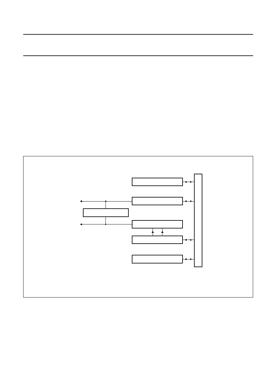
2001 Apr 17
37
Philips Semiconductors
Product specification
Digital telephone answering machine chip
PCD6001
10.11 I
2
C-bus
The serial port I
2
C-bus is a simple bidirectional 2-wire bus
for efficient inter IC data exchange. The I
2
C-bus consists
of a data line (SDA) and a clock line (SCL). These lines
also function as I/O Port P1.7 and P1.6 respectively.
The system is unique because data transport, clock
generation, address recognition and bus arbitration are all
controlled by hardware. The I
2
C-bus serial I/O has
complete autonomy in byte handling and supports all four
I
2
C-bus operating modes:
∑
Master transmitter
∑
Master receiver
∑
Slave transmitter
∑
Slave receiver.
The I
2
C-bus block contains 4 SFR registers. The mode of
operation is controlled by the S1CON register. S1STA is
the status register whose contents may also be used as a
vector to various service routines. S1DAT is the data shift
register and S1ADR is the slave address register. Slave
address recognition is performed by hardware.
An application note is available to help implementation of
the software for the I
2
C-bus.
handbook, full pagewidth
MGM777
S1ADR
DATA SHIFT REGISTER
S1DAT
SDA
BUS ARBITRATION LOGIC
SCL
BUS CLOCK GENERATOR
MICROCONTROLLER ASF GROUP INTERFACE
S1CON
SERIAL CONTROL REGISTER
STATUS REGISTER
OWN ADDRESS REGISTER
S1STA
Fig.13 I
2
C-bus serial I/O.
2001 Apr 17
38
Philips Semiconductors
Product specification
Digital telephone answering machine chip
PCD6001
10.11.1 S
ERIAL
C
ONTROL
R
EGISTER
(S1CON)
Two bits are affected by the I
2
C-bus hardware, the SI bit is set to logic 1 when a serial interrupt is requested, and the
STO bit is set to logic 0 (cleared) when a STOP condition is present on the I
2
C-bus. The STO bit is also cleared when
ENS1 = 0. When the I
2
C-bus block is in the Master mode the serial clock frequency is determined by the clock rate bits
CR[2:0].
Table 33 Serial Control Register (SFR address D8H)
Table 34 Description of S1CON bits
7
6
5
4
3
2
1
0
CR2
ENS1
STA
STO
SI
AA
CR1
CR0
BIT
SYMBOL
DESCRIPTION
7
CR2
Clock rate. This bit along with bits CR1 and CR0 determines the serial clock frequency
when I
2
C-bus is in Master mode, see Table 35.
6
ENS1
When this bit is set to logic 0 the I
2
C-bus is disabled, outputs SDA and SCL are in the
high-impedance state, and P1.6 and P1.7 function as open-drain ports. With this bit set
to logic 1 the I
2
C-bus is enabled. The P1.6 and P1.7 port latch must be set to logic 1.
5
STA
Start flag. When the STA bit is set to logic 1 in Slave mode, the I
2
C-bus hardware
checks the status of the I
2
C-bus and generates a START condition if the bus is free. If
STA is set to logic 1 while the I
2
C-bus is in Master mode, the I
2
C-bus transmits a
repeated START condition.
4
STO
Stop flag. With this bit set to logic 1 while in Master mode a STOP condition is
generated. When a STOP condition is detected on the bus, the I
2
C-bus hardware clears
the STO flag. In the Slave mode, the STO flag may also be set to logic 1 to recover from
an error condition. In this case no STOP condition is transmitted to the I
2
C-bus.
However, the I
2
C-bus hardware behaves as if a STOP condition has been received and
releases SDA and SCL. The I
2
C-bus then switches to the `not addressed' receiver
mode. The STO flag is automatically cleared by hardware.
3
SI
I
2
C-bus interrupt flag. When this flag is set to logic 1, an acknowledge is returned (i.e.
an interrupt is generated) after any one of the following conditions:
∑
A start condition is generated in Master mode
∑
Own slave address received during AA = 1
∑
General call address received while S1ADR[0] = 1and AA = 1
∑
Data byte received or transmitted in Master mode (even if arbitration is lost)
∑
Data byte received or transmitted as selected slave
∑
Stop or start condition received as selected slave receiver or transmitter.
2
AA
Assert Acknowledge. When set to logic 1 an acknowledge will be returned during the
acknowledge clock pulse on SCL when:
∑
Own slave address is received
∑
General call address is received while S1ADR[0] = 1
∑
Data byte is received while device is a selected slave.
With AA = 0 no acknowledge will be returned. Consequently, no interrupt is requested
when the `own slave address' or general call address is received.
1
CR1
Clock rate. These 2 bits along with the CR2 bit determine the serial clock frequency
when I
2
C-bus is in Master mode, see Table 35.
0
CR0
2001 Apr 17
39
Philips Semiconductors
Product specification
Digital telephone answering machine chip
PCD6001
Table 35 I
2
C-bus bit frequencies in Master mode
Note that any I
2
C-bus device tolerates a maximum and sometimes a minimum SCL frequency. The correct setting of bits
CR2, CR1 and CR0 using a specific microcontroller clock frequency is therefore important.
10.11.2 S
TATUS
R
EGISTER
(S1STA)
S1STA is an 8-bit read-only register. Its contents may be used as a vector to a service routine. This optimizes the
response time of the software and consequently the I
2
C-bus.
Table 36 Status Register (SFR address D9H); reset state F8H
10.11.3 D
ATA
S
HIFT
R
EGISTER
(S1DAT)
S1DAT contains the serial data to be transmitted or data that has just been received. Bit 7 is transmitted or received first.
Table 37 Data Shift Register (SFR address DAH); reset state 00H
10.11.4 A
DDRESS
R
EGISTER
(S1ADR)
This 8-bit `own address register' may be loaded with the 7-bit address to which the controller will respond when
programmed as a slave receiver/transmitter. The LSB bit GC is used to determine whether the general CALL address is
recognized.
Table 38 Address Register (SFR address DBH); reset state 00H
CR2
CR1
CR0
f
microcontroller_clk
DIVIDED BY
I
2
C-BUS BIT FREQUENCY (kHz) at f
microcontroller_clk
0.9 MHz
3.58 MHz
7.16 MHz
14.32 MHz
21 MHz
0
0
0
10
90
358
-
-
-
0
0
1
20
45
179
358
-
-
0
1
0
30
30
119
239
-
-
0
1
1
40
22
90
179
358
-
1
0
0
80
11
45
89.5
179
269
1
0
1
120
7.5
30
59.7
119
179
1
1
0
160
5.6
22
44.8
89.5
134
1
1
1
-
-
-
-
-
-
BIT
SYMBOL
DESCRIPTION
7 to 3
SC[4:0]
contains the status code defined by the I
2
C protocol
2 to 0
-
not used, all bits are 0
BIT
SYMBOL
DESCRIPTION
7 to 0
S1DAT[7:0]
I
2
C-bus serial data
BIT
SYMBOL
DESCRIPTION
7 to 1
SLA[6:0]
own I
2
C-bus address
0
GC
0: general CALL address is not recognized
1: general CALL address is recognized

2001 Apr 17
40
Philips Semiconductors
Product specification
Digital telephone answering machine chip
PCD6001
10.12 MSK modem
The MSK modem is used for in-band signalling between
handset and base in analog cordless telephone systems
CT0, CT1 and CT1+. The MSK modems receiver and
transmitter can be enabled separately. Receive and
transmit interrupts can wake-up the microcontroller during
its power saving Idle mode. The baud rates are
programmable between 1200 and 4800 baud. Figure 14
shows the functional diagram of the MSK modem.
The MIN input is the alternative input of P3.7 and
MOUT[2:0] is the alternative output of P3.0, P3.1 and
P3.6. The RX and TX mute can be done in software by any
pin of MA, P1, P3 and P2. The MTI and MRI interrupts are
OR-ed together to a single interrupt called msk_int. So the
msk_in interrupt handler should investigate the status of
the MRI and MTI bit in the MCON SFR.
The MOUT[2:0] outputs and the MIN input are alternative
functions of P3.0, P3.1, P3.6 and P3.7. The MOUT[2 :0]
outputs are `111' when the MSK transmitter is disabled
(default after reset). Therefore, P3.0, P3.1, P3.6 and P3.7
can still be used as general purpose I/O ports. Setting bit 7
of MSTAT will invert the MIN polarity.
The modem has the following features:
∑
Full-duplex operation via 8-bit parallel interface; the
message is fully Manchester coded/decoded
∑
Automatic detection of 16 bit Manchester preamble
pattern
∑
The last received 4 bits of the preamble pattern are
programmable
∑
Receiver full, transmitter empty indication bits
∑
Manchester coding and decoding for clock recovery and
early error detection
∑
Programmable input polarity
∑
Baud rate selection from 1200, 2400, 3600
and 4800 baud with internal modem timer
∑
Receiver and transmitter off-states with no power
consumption.

2001 Apr 17
41
Philips Semiconductors
Product specification
Digital telephone answering machine chip
PCD6001
handbook, full pagewidth
MGT434
MPOL
RECEIVER
TRANSMITTER
MOUT0
MOUT1
MOUT2
R2
R1
R0
RF
RF
SLICER
MIN
VOUT
MSTAT
MPR
MCLK
MRI
IBD7 to IBD0
AN7 to AN0
MSK_INT
MTI
MB0
MB1
MREN
MTEN
MBUF
MCON
TIMER
MSK MODEM
80C51 CORE
earpiece
mouthpiece
RX_MUTE
TX_MUTE
Fig.14 MSK modem functional diagram.

2001 Apr 17
42
Philips Semiconductors
Product specification
Digital telephone answering machine chip
PCD6001
10.12.1 80C51
MICROCONTROLLER INTERFACE
.
The modem block interfaces to the microcontroller via the interrupt signal MSK_INT and via the control and data SFRs
MCON, MSTAT and MBUF. The MSK modem receive and transmit registers are both accessed via the SFR MBUF.
Writing to MBUF loads the transmit register and reading MBUF accesses a physically separate receive register.
10.12.1.1 MSK Modem Control Register (MCON)
Table 39 MSK Modem Control Register (SFR address C8H)
Table 40 Description of MCON bits
Note
1. If both the transmitter and the receiver are disabled (MTEN = 0 and MREN = 0), the clock of the MSK modem is
switched off. It is advised to use this state for power saving.
Table 41 Selection of the modem's baud rates
10.12.1.2 MSK Modem Status Register (MSTAT)
Table 42 MSK Modem Status Register (SFR address CAH), reset state 00H
7
6
5
4
3
2
1
0
MPR3
MPR2
MPR1
MPR0
MB1
MB0
MTEN
MREN
BIT
SYMBOL
DESCRIPTION
7 to 4
MPR[3:0]
Preamble pattern. These 4 bits define the modems preamble pattern.
3 to 2
MB[1:0]
RX/TX frequency. These 2 bits define the modem transmit/receive frequency; see
Table 41.
1
MTEN
Modem Transmitter Enable. If set the transmitter is active and MOUT[2:0] will get the
value <100> if no data is transmitted. If reset, MOUT[2:0] will get the value <111> to
zero the currents in the resistive DAC; see note 1.
0
MREN
Modem Receiver Enable. If set the modem receiver is active and scans for Manchester
data; see note 1.
MB1
MB0
MODEM BAUD RATE
0
0
1200 baud
0
1
2400 baud
1
0
3600 baud
1
1
4800 baud
7
6
5
4
3
2
1
0
MPOL
-
MRF
MRE
MRP
MRL
MTI
MRI

2001 Apr 17
43
Philips Semiconductors
Product specification
Digital telephone answering machine chip
PCD6001
Table 43 Description of MSTAT bits
10.12.1.3 MSK Modem Data Buffer (MBUF)
Table 44 MSK Modem Data Buffer (SFR address C9H)
Table 45 Description of MBUF bits
BIT
SYMBOL
DESCRIPTION
7
MPOL
MIN polarity switch. If MPOL = 1, the value of the MIN pin is inverted before being
applied to the MSK block.
5
MRF
Modem receiver full flag. This bit is set when MBUF holds a newly received byte. MRF
is reset if the receiver is disabled (MREN = 0) or by reading MBUF. This bit is read-only.
Writing to it will have no effect.
4
MRE
Modem Receiver Error flag. Indicates the reception of a non-Manchester bit. This bit is
set by hardware and is reset by reading MBUF, by disabling the receiver (MREN = 0) or
by resetting MRI. This bit is read-only. Writing to it will have no effect.
3
MRP
Modem Receiver Preamble flag. This bit is set by hardware when the modem
recognized the programmed preamble pattern (AAAH, MPR3 to MPR0) after locking the
receiver clock (MRL = 1). MRP is reset by hardware if the receiver is disabled
(MREN = 0) or if non-Manchester data is received (MRE = 1). This bit is read-only.
Writing to it will have no effect.
2
MRL
Modem Receiver Clock Locked flag. This bit is set when the clock of the receiver is
locked, i.e. when the receiver has detected Manchester data but has not found the
preamble pattern yet. MRL is reset when the receiver detects a non-Manchester bit or
when the receiver is disabled. This bit is read-only. Writing to it will have no effect.
1
MTI
Modem Transmit Interrupt flag. Indicates MBUF is empty to accept a new byte for
transmission. This bit is reset by writing to MBUF or by writing a 0 to it. Writing a 1 to
MTI will set the bit. This allows to generate a hardware interrupt by software.
0
MRI
Modem Receive Interrupt flag. Indicates:
Modem Receiver Full (MRF = 1) or
Modem Receiver Error (MRE = 1) or
Modem Receiver Preamble (MRP = 1) or
Modem Receiver Clock Locked (MRL = 1)
This bit is reset by reading MBUF or by writing a logic 0 to MRI. A reset of MRI will also
reset MRE. Writing a logic 1 to MRI will have no effect.
7
6
5
4
3
2
1
0
D7
D6
D5
D4
D3
D2
D1
D0
BIT
SYMBOL
DESCRIPTION
7 to 0
D7 to D0
Writing to MBUF will load the data in the transmit buffer and automatically start a
transmission at MOUT if the transmitter is enabled (MTEN = 1). A new byte can be
loaded after MTI is set. If a new byte is loaded before the setting of MTI then the
previous byte will be lost. After data has been received at MIN, indicated by MRI, the
received byte can be read from MBUF.
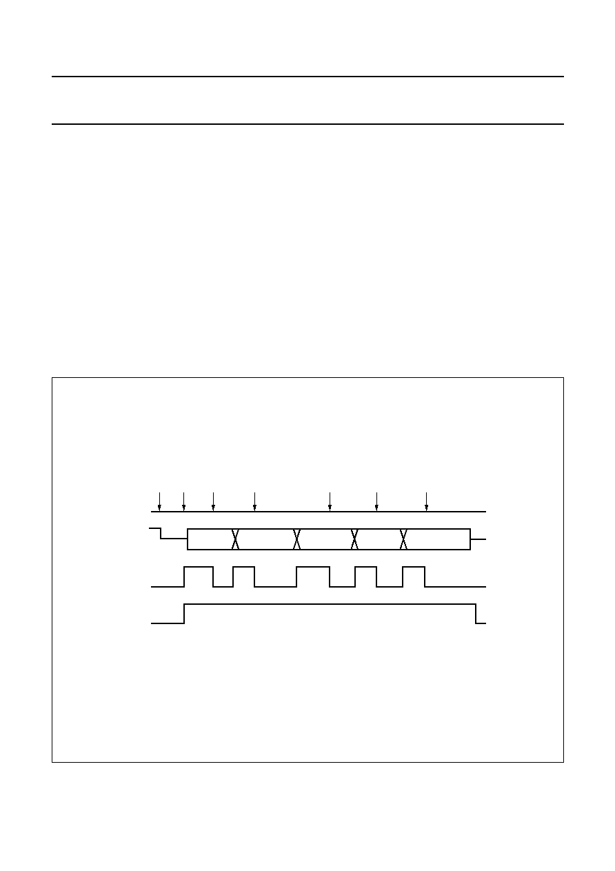
2001 Apr 17
44
Philips Semiconductors
Product specification
Digital telephone answering machine chip
PCD6001
10.12.2 D
ATA TRANSMISSION
Data transmission is enabled if bit MTEN in register MCON
is set to logic 1. If MTEN is logic 0 data transmission is
disabled and MOUT[2:0] is set to <111> to zero the
currents in the resistive DAC. Setting MTEN to logic 1 sets
MOUT[2:0] to the Idle value <100>. This results in a value
close to 0.5V
DD
on the output signal of the external DAC.
Transmission is started by loading the first byte into
register MBUF. All bytes are transmitted starting with the
MSB.
A message is transferred in a block of 3 or more bytes, the
first two bytes being the programmed Manchester
preamble pattern. In order to insert the preamble pattern,
the first two bytes AAH and AxH (with x being the
MPR[3:0] values programmed in the receiver MSK
modem) have to be written to MBUF by software. After
this, the first byte of the message is written to MBUF.
As soon as MBUF is ready to accept new input, signal MTI
is set. A new byte written to MBUF automatically clears
MTI. The time between two MTI interrupts is:
(e.g. for 1200 baud, T = 6.7 ms).
If no new byte is written to MBUF at the end of a byte
transmission, the modem transmitter stops transmission
and MOUT[2:0] is set to the Idle state <100>. In this case
MTI must be cleared explicitly. If MTEN is reset during
transmission, the transmitter will finish the transmission of
the current byte and then will set MOUT[2:0] to the off state
<111>. No interrupt on MTI will be generated at the end of
the transmission.
During reception, a digital PLL re-synchronizes on the
active transition of every bit. This allows a continuous
transmission of long messages. Figure 15 shows a
possible timing diagram of data transmission.
T
8
1
baud rate
------------------------
◊
=
handbook, full pagewidth
MGM779
data ADH
data AAH
data AAH
data 55H
data 55H
write
MBUF
55H
write
MBUF
55H
80C51
access
MOUT
MTI
TX_MUTE
set
MTEN
clear
MTI
write
MBUF
AAH
write
MBUF
AAH
write
MBUF
ADH
Fig.15 Data transmission timing diagram.

2001 Apr 17
45
Philips Semiconductors
Product specification
Digital telephone answering machine chip
PCD6001
10.12.3 D
ATA RECEPTION
A message is received as a block of one or more data
bytes. When enabled, the receiver starts sampling MIN
and tries to detect a Manchester pattern. As soon as
3 consecutive Manchester bits are detected the receiver
clock is locked (MRL = 1) and the receiver starts scanning
the incoming data for the programmed Manchester
preamble pattern. When the modem recognizes the
preamble pattern, bit MRP is set to logic 1. If a
non-Manchester bit is detected before finding the
preamble pattern then MRL is reset and MRE is set to
logic 1. The synchronization process has to restart. If the
preamble pattern has been detected the receiver starts to
Manchester decode the incoming data bits and shifts them
into an internal register. After eight bits the contents of the
internal register are copied to MBUF and MRF bit is set to
logic 1. The received byte can be read from MBUF while
receiving continues in the internal register. If a
non-Manchester bit is received during data reception then
MRE is set to logic 1 and MRL and MRP are reset. The
receiver has to resynchronize before receiving new data.
Whenever one of the bits MRF, MRE, MRP and MRL is set
the MRI bit is also set and an MRI interrupt is generated.
This means that when an MRI interrupt occurs the 4 status
bits have to be polled by software. The bit MRL allows the
software to decide very quickly whether an occupied
channel contains Manchester coded data or not. The MRP
bit is used to find the start of data transmission in a
message that is repeated over and over again. MRE is
used to detect a Manchester error, which is a violation of
the Manchester coding rule that the received level should
change in the middle of a bitcell. The MRF bit indicates that
the data in MBUF is ready to be read by the software.
During data reception the time between two settings of
MRF (each one generating an MRI interrupt) is;
Figure 16 shows an example of the timing diagram of data
reception.
T
8
1
baud rate
------------------------
◊
=
handbook, full pagewidth
MGM780
data
37
data
AA
data
AD
data
1F
data
37
non-Manchester
(speech)
non-Manchester
(speech)
read
MBUF
1F
read
MBUF
37
clear
MRI
clear
MRI
clear
MRI
RX_MUTE should be
generated by microcontroller
upon interrupt
RX_MUTE should be
cleared by microcontroller
at end of message
write
MREN = 1
80C51
access
MIN
MRI
MRF
MRL
MRP
MRE
Fig.16 Data reception timing diagram.
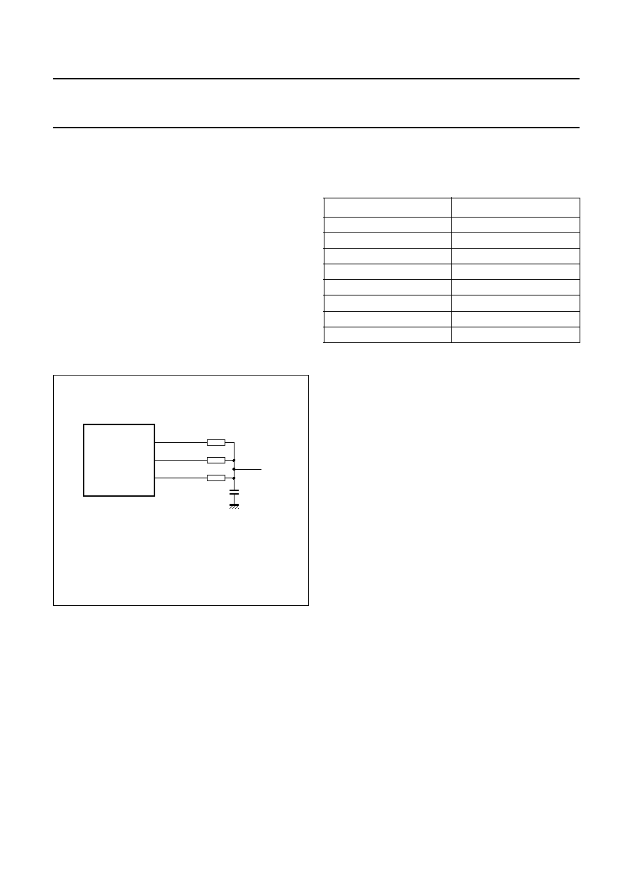
2001 Apr 17
46
Philips Semiconductors
Product specification
Digital telephone answering machine chip
PCD6001
10.12.4 M
ANCHESTER CODING OF DATA
The bits of the data byte written in MBUF are Manchester
encoded as shown in Fig.17. A logic 1 is coded as a
LOW-to-HIGH transition in the middle of a bitcell, a logic 0
is coded as a HIGH-to-LOW transition.The Manchester
encoded signal contains redundancy for early error
detection in received bits. A non-matching 1 and 0 or
0 and 1 pair indicates an error condition.The Manchester
encoded signal has a polarity change in each bitcell.
10.12.5 W
AVEFORM GENERATION WITH
MOUT[2:0]
The 3 digital output pins MOUT[2:0] should be used as an
input to a 3-bit external DAC. The signals can be
connected via external resistors R2, R1 and R0 to a
summation point and then be filtered with an external
capacitor C1. This 3-bit DAC is shown in Fig.17.
Table 46 gives the relationship between MOUT[2:0] and
the voltage VOUT.
Table 46 VOUT as a function of MOUT[2:0]; note 1
Note
1. Resistor values are shown in Fig.17.
Figure 18 shows the possible waveforms that are
produced by the waveform generator. The horizontal axis
shows the sample counter on which the waveform
changes its value. Each bit is built-up out of 2
◊
40
samples (n
◊
3.456 MHz crystal, CKCON.6 = 0) or 2
◊
42
samples (3.58 MHz, CKCON.6 = 1). The vertical axis
shows the values of MOUT[2:0], forming the inputs of the
resistive DAC. The first half of the waveform is determined
by the previous and the current bit, whereas the second
half of the waveform is determined by the current and the
next bit to be transmitted. The count frequency of the
sample counter depends on the programmed baud rate.
If the transmitter is disabled with MTEN set to logic 0,
MOUT[2:0] is <111> to save power in the resistive DAC.
If the transmitter is enabled and no data is transmitted,
MOUT[2:0] has an idle value of <100>, which corresponds
to 0.57V
DD
.
handbook, halfpage
MGM781
R0
WAVEFORM
GENERATOR
MOUT0
R1
MOUT1
VOUT
R2
MOUT2
C1
10 nF
Fig.17 3-bit DAC with MOUT[2:0].
R0 = R
R1 = 0.48
◊
R
R2 = 0.25
◊
R
MOUT[2:0]
VOUT
000
0
001
0.14V
DD
010
0.29V
DD
011
0.43V
DD
100
0.57V
DD
101
0.71V
DD
110
0.86V
DD
111
V
DD

2001 Apr 17
47
Philips Semiconductors
Product specification
Digital telephone answering machine chip
PCD6001
handbook, full pagewidth
MGM787
111
101
011
001
010
3
6
10
30
34 37 40
46
53
61
80
000
100
110
001
53
61
111
101
011
001
010
3
6
10
30
34 37 40
46
80
000
100
110
110
111
101
011
001
010
3
6
10
30
34 37 40 43 46
50
70
74
77 80
000
100
110
111
111
101
011
001
010
19
27
34
40 43 46
50
70
74
77 80
000
100
110
100
111
101
011
001
010
19
27
34
40
46
53
61
80
000
100
110
101
111
101
011
001
010
3
6
10
30
34 37 40 43 46
50
70
74
77 80
000
100
110
000
111
101
011
001
010
19
27
34
40
46
53
61
80
000
100
110
010
43
111
101
011
001
010
19
27
34
40
46
50
70
74
77 80
000
100
110
011
Fig.18 Waveforms with MOUT[2:0] for previous, current and next bits to be transmitted.

2001 Apr 17
48
Philips Semiconductors
Product specification
Digital telephone answering machine chip
PCD6001
10.12.6 S
YNCHRONISATION
When enabled the receiver samples MIN with a frequency
f = 8
◊
baud rate. The sampled values are shifted into an
8-bit shift register. This register is regularly checked
whether it contains samples that fulfil the Manchester
coding rule i.e. whether there is a LOW-to-HIGH or a
HIGH-to-LOW transition in the middle of the bitcell. The
receiver searches for 3 consecutive sets of 8 samples that
fulfil the Manchester coding rule. If these sets have been
found the clock is locked (MRL = 1) and the receiver starts
looking for the Manchester preamble pattern. From this
point on the receiver uses a Phase Locked Loop (PLL) to
adjust the synchronisation after each received Manchester
bit.
10.13 LE control
The LE signal is the alternative output of P4.0 and can be
turned on with ALTP bit 1. The LE signal can be used to
connect to the E input of 68xxx microcontroller compatible
peripherals such as an LCD controller. If these peripherals
have a slow access time the LE signal can be made HIGH
earlier by setting bit 0 of ALTP. Bit 0 of ALTP will be
cleared by hardware after the execution of a MOVX
instruction. The ALTP register is described in more detail
in Section 16.2.
Figure 19 shows the LE signal shapes for early read
and/or write when the P4.0 alternative port function for LE
is selected. In Fig.19, the DTAM WR signal is only shown
for timing reference.
Neither WR nor RD are physically connected to the
display. The display RS and R/W pin can be connected to
Port 2 or MA pins (logic 0 after reset) and controlled by
software. The early LE timing hardware makes it possible
to access LCD drivers (or other peripheral devices with the
same interface) which require a large access time
(>3
◊
microcontroller_CLK).
The display LE pin (P4.0) rising edge is determined by
software, by setting bit 0 and 1 of the ALTP SFR. In order
to latch the Port 0 data at the correct moment, the falling
edge is determined by internal DTAM hardware. This
generates for the LCD write operation an LE falling edge
at 0.5 of a microcontroller clock before the falling edge of
WR, such that the LCD data hold time (t
h
) requirement is
always fulfilled.
Figure 20 shows the LE signal shape for normal read
and/or write when the P4.0 alternate port function for LE is
selected. Again, the DTAM WR signal is only shown for
timing reference. Both the rising and falling edges of the
display LE pin (P4.0) are determined by hardware if only
bit 1 of the ALTP SFR is set. This generates for the LCD
write operation an LE falling edge at 0.5 of a
microcontroller clock before the falling edge of WR, such
that the LCD data hold time (t
h
) requirement is always
fulfilled.
The normal LE timing is actually the inverted value of
either the RD or WR signal. This timing can be used for
peripheral devices that have an access time of less than
3
◊
microcontroller_CLK.
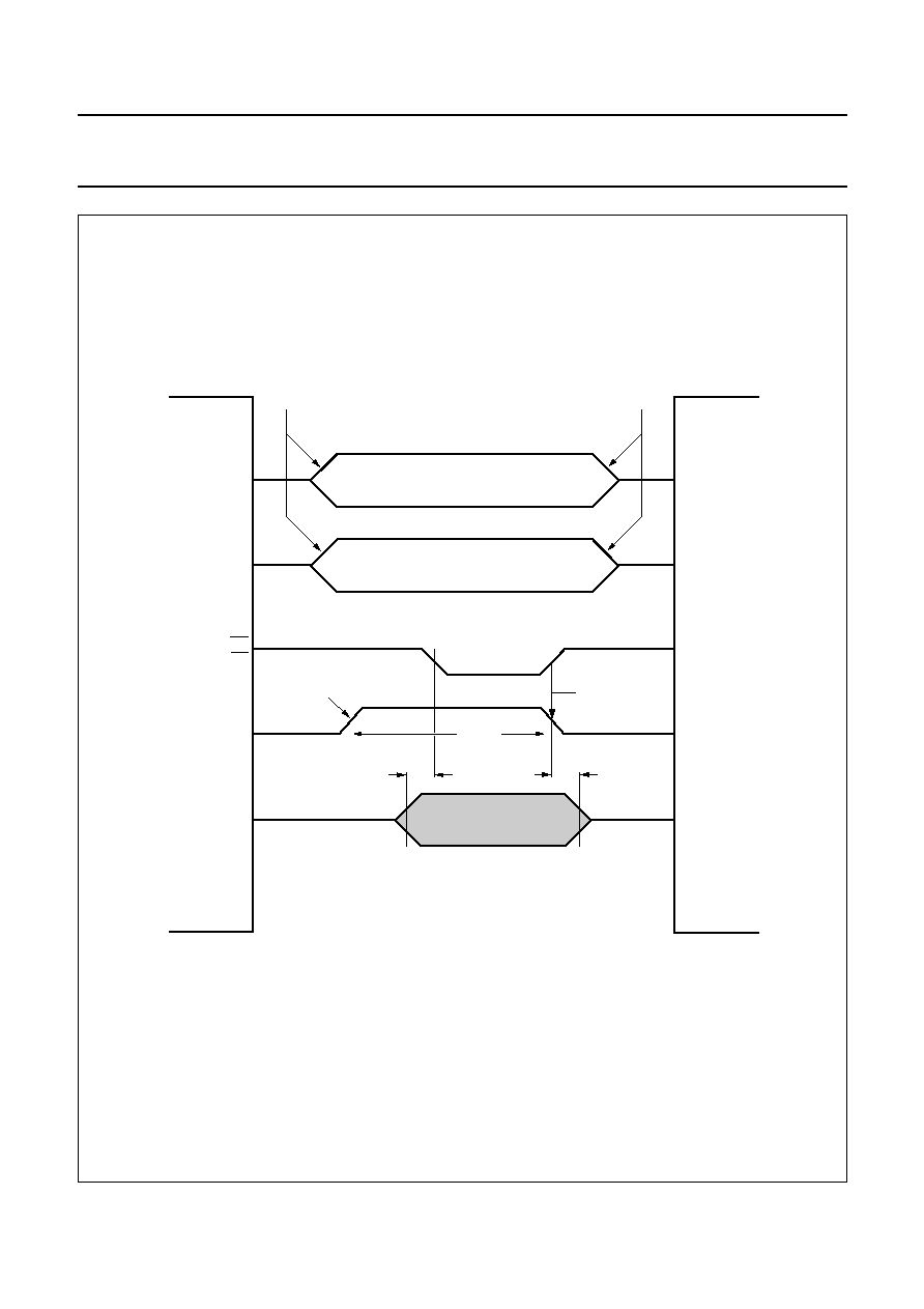
2001 Apr 17
49
Philips Semiconductors
Product specification
Digital telephone answering machine chip
PCD6001
handbook, full pagewidth
MGT435
PCD6001
LCD
MAx
MAy
LE
P00 to P07
RS
R/W
n.c.
E
DB0 to DB7
software controlled
edge timing
software controlled
rising edge timing
hardware controlled
falling edge timing
software controlled
edge timing
command
data
DATA
read
write
>
400 ns
1/2
µ
C_CLK
1
µ
C_CLK
(RD)
WR
Fig.19 Early LE timing.

2001 Apr 17
50
Philips Semiconductors
Product specification
Digital telephone answering machine chip
PCD6001
handbook, full pagewidth
MGT436
PCD6001
LCD
MAx
MAy
LE
P00 to P07
RS
R/W
n.c.
E
DB0 to DB7
software controlled
edge timing
hardware controlled
rising edge timing
hardware controlled
falling edge timing
software controlled
edge timing
command
data
DATA
read
write
1/2
µ
C_CLK
1
µ
C_CLK
(RD)
WR
Fig.20 Normal LE timing.

2001 Apr 17
51
Philips Semiconductors
Product specification
Digital telephone answering machine chip
PCD6001
11 DSP I/O REGISTERS
For the DTAM application, the DSP is connected with
several peripherals as shown in Fig.21. Basically, the DSP
is connected to the analog interfaces CODEC1 and
CODEC2.
The DSP communicates with the peripherals via the
DSP I/O registers. The data transfer is performed by the
16-bit XD data bus. The I/O registers of the different
I/O units are 16 bits wide.
The microcontroller controls the DSP and is the link
between an external speech memory and the DSP. The
TICB provides the FS1 clock, which interrupts the DSP
every 125
µ
s.
11.1
Interface to CODEC
The CODEC data buffers are used to exchange speech
data between the DSP and the CODECs (see Fig.21). The
digital decimation filter DDF writes equidistant in time
16-bit linear PCM samples to the DSP I/O registers
CDC_DI0 to CDC_DI3 (address 01H to 04H for CODEC1
and address 09H to 0CH for CODEC2) at a rate of 32 kHz.
The Digital Noise Shaper (DNS) reads equidistant in time
16-bit linear PCM samples from the DSP I/O registers
CDC_DO0 to CDC_DO3 (address 05H to 08H for
CODEC1 and address 0DH to 10H for CODEC2) at a rate
of 32 kHz. The input registers CDC_DI0 to CDC_DI3 and
the output registers CDC_DO0 to CDC_DO3 are also
called data input/output DIO registers.

2001 Apr 17
52
Philips Semiconductors
Product specification
Digital telephone answering machine chip
PCD6001
handbook, full pagewidth
MGM785
00H DTMC
00H MTDC
IOA4 to IOA0
D15 to D0
MTDD
DTMD
80C51
IOMDI
IOMDO
IOMC
CDC1_DI0
CDC1_DI1
CDC1_DI2
CDC1_DI3
CDC1_DO0
CDC1_DO1
CDC1_DO2
CDC1_DO3
CDC2_DI0
CDC2_DI1
CDC2_DI2
CDC2_DI3
CDC2_DO0
CDC2_DO1
CDC2_DO2
CDC2_DO3
IOSR
I/O CONTROL BLOCK
DNS
DDF
DNS
DDF
DSP_IACK
FSEO
FSC
FSC
DCK
DO
DI
DCK
TICB
REAL 16010
DSP CORE
IOM
OR
DIGITAL CODEC1
(LINE CODEC)
analog
section
CODEC1
DIGITAL CODEC2
(HANDSFREE CODEC)
analog
section
CODEC2
IACK
IORQ
DATA MEMORY
IOC IOA
IOD
Fig.21 DSP I/O architecture.

2001 Apr 17
53
Philips Semiconductors
Product specification
Digital telephone answering machine chip
PCD6001
12 EXTERNAL MEMORY INTERFACE
The external memory interface consists of the interface from the 80C51 microcontroller to external flash memory and
software debugging circuitry such as a Metalink emulator or target debugger. The external memory interface is shown in
Fig.22.
handbook, full pagewidth
MGT456
80C51
MCB
and
P4
EA
ALE
P0_INT
P2_INT
ARD
ALE
RST
P4.3
RD
WR
PSE
P4.1/FSK
P4.2/FSO
P4.4/FSI
P4.0/LE
P4.5/GPC
WNCAD
SCK/CLE
DI/ALE
DO
PSEN
E_LCD
P0
P0
P1
P3
MA
P2
MA
P2
IO7 to IO0
CENFLASH
OENCAD
FLASH
and
LCD
OTP
PCD6001
EXTERNAL
MEMORY
INTERFACE
control
XRAM MAPPED
REGISTERS
Fig.22 External memory interface.

2001 Apr 17
54
Philips Semiconductors
Product specification
Digital telephone answering machine chip
PCD6001
The internal ROM fetching will be activated by making EA
a logic 1. If EA is logic 0 external program memory can be
connected and the internal ROM will be disabled. The
external memory interface block contains the MA and P2
generation logic and registers.
The P2 and MA latches have special enable signals.
Appropriate bits (MAGP and P2GP) in the control register
make P2 and MA available as general purpose output
ports or as the 80C51 address bus. The last option is
necessary for target debugging (EA = 0), external ROM
(EA = 0) or parallel flash memory (MAGP = 1 and
P2GP = 1). In these cases external latches must be
provided if the application needs the P2/MA as general
purpose output ports as well.
The MAGP and P2GP signals are bit 3 and 4 of the
configuration register latch. MA will be a general purpose
output port when MAGP is set to logic 0 by software
(default after reset). If MAGP is set to logic 1 the MA port
operates as the lower 8 bits of the program/data address
bus. P2 will be a general purpose output port when P2GP
is set to logic 0 by software (default after reset). If P2GP is
set to logic 1 the P2 port operates as the higher 8 bits of
the program/data address bus. The accessability of the
P2GP and MAGP bits of the ConfReg register in the
external interface block depends on the value of the EAM
(P4CFG.5) SFR bit: when EAM is logic 0 (default after
reset), the XRAM-mapped control registers can only be
accessed if P4.3 is logic 1 (compatible mode to PCD6002
DTAM device). Otherwise (i.e. when EAM is logic 0),
XRAM addressing is independent of the value of the P4.3
SFR bit, but needs ARD to be logic 0 (only available when
fetching from internal memory, i.e. EA is logic 1).
The latches are used for the configuration, MA and
P2 registers and they are mapped at addresses
200H to 202H of the external data memory map. Refer to
Table 48.
∑
Register ConfReg (2-bit): this is the Configuration
Register. In this register single bits are set to control the
functionality of the external outputs. The content of this
register is given in Table 49. With the bits P2GP
(P2 General Purpose) and MAGP (MA General
Purpose) the output function of MA and P2 is
determined.
With bit P2GP = 0 (reset value) the output P2 is latched
and can be used as a general purpose output for
example to drive LEDs. Data can be written to the
register P2 with a MOVX command. With P2GP = 1 the
internal bus P2_int[7:0] is directly transferred to the
output P2[7:0]. This mode is for example applied when
using parallel flash. Output P2[7:0] delivers then the
high address byte for the parallel flash.
With MAGP = 0 (reset value MAGP = 0) the output
MA[7:0] can be used as a general purpose output.
Otherwise, output MA[7:0] serves as latch (with ALE as
enable signal) for the low address byte provided by a
internal bus.
∑
Register MA (8-bit): If EA = 1 (internal ROM used) and
MAGP = 0 (default after reset) the MA pins will output
the contents of the MA register (0201H) which contains
00H after reset. The state of the MA pins can be
changed by writing a new value to the MA register. This
must be done with a MOVX instruction while the P4.3 bit
or the EAM bit is logic 1.
∑
Register P2 (8-bit): If EA = 1 (internal ROM used) and
P2GP = 0 (default after reset) the P2 pins will output the
contents of the P2 register (0202H) which contains 00H
after reset. The state of the P2 pins can be changed by
writing a new value to the P2 register.This must be done
with a MOVX instruction while the P4.3 bit or the EAM
bit is logic 1.
Table 47 Overview of P0/MA/P2 settings; notes 1, 2, 3, 4 and 5
Notes
1. XA/XD: address and data during a MOVX instruction; PA/PD: address and data during a code fetch; GP: general
purpose port; low: low address byte; high: high address byte.
EA
MAGP
P2GP
FUNCTION P0/MA/P2
0
X
X
P0 = XA_low/XD/PA_low/PD, MA = XA/PA_low and P2 = XA/PA_high
1
0
0
P0 =XD, MA =GP and P2 = GP
1
1
0
P0 = XD, MA = XA_low and P2 = GP
1
0
1
P0 = XD, MA = GP and P2 = XA_high
1
1
1
P0 = XD, MA = XA_low and P2 = XA_high

2001 Apr 17
55
Philips Semiconductors
Product specification
Digital telephone answering machine chip
PCD6001
2. Writing MAGP/P2GP is independent of the setting of the P4.3 SFR bit if P4CFG.5 (EAM) is set to logic 1, otherwise
(EAM logic 0) P4.3 must be logic 1.
3. The WR/RD pins are always active when doing a MOVX. They can be turned inactive for MOVX below 200H by
setting the ARD bit in PCON in case the EAM Bit is set to logic 1.
4. P0/P2 are standard 80C51 ports. An external latch is not needed since the demultiplexing of P0 is taken over by the
MA port.
5. The MA/P2/ConfReg registers are part of the auxiliary RAM address space and can be disabled by setting the ARD
bit in PCON in case the EAM Bit is set to logic 1.
Table 48 External memory control registers
Table 49 Configuration Register (ConfReg); reset state 00H
12.1
Supported flash memories
Table 50 shows the ports that are available in an application using various flash memories.
For all types of flash memory shown in Table 50 (except for the parallel flash memory) at least 34 general purpose
I/O pins can be used for the application (display, line interface, keypad and LEDs; for example). P0 can also be used for
the application to connect memory mapped peripherals such as an LCD controller or keypad. P0 pins have no output
latch, so data written to this port will not remain here.
There are many different types of flash memories manufactured, and the PCD6001 will work with many of them. Table 51
explains the most important characteristics of a few of the commercially available flash memories which can be
connected to the PCD6001 directly.
Table 50 Ports available for the application
Note
1. P0 can be used as a data bus for other peripherals if not conflicting with the flash memory.
EXTERNAL MEMORY CONTROL
REGISTERS
ADDRESS P2/P0
(P4.3 = 1, EAM = 0
or ARD = 0, EAM = 1, EA = 1)
RESET VALUE
ACCESS
ConfReg
0200H
00H
R and W
MA
0201H
00H
R and W
P2
0202H
00H
R and W
7
6
5
4
3
2
1
0
-
-
-
P2GP
MAGP
-
-
-
FLASH
MEMORY
PORTS USED BY FLASH
PORTS AVAILABLE FOR APPLICATION
I/O
I
O
I/O
I/O
O
CAD
P0
-
P4.1, P4.2 and P4.3
P1, P3, P4.0,
P4.4 and P4.5
P0
(1)
MA and P2
SPI/Microwire
-
P4.4
P4.1, P4.2 and P4.3
P1, P3,
P4.0 and P4.5
P0
MA and P2
I
2
C-bus
P1.6 and P1.7
-
-
P1, P3 and P4
(except P4.3)
P0
(1)
MA, P2 and P4.3
Parallel
P0
-
MA, P2, P4.0, P4.1,
P4.2 and P4.3
P1, P3,
P4.4 and P4.5
P0
(1)
-

2001
Apr
17
56
Philips Semiconductors
Product specification
Digital telephone ans
w
e
r
ing machine chip
PCD6001
Table 51 Selection of supported flash devices
Notes
1. Supported by Philips PCD6001 API 1.x software (not all are necessarily supported in parallel at runtime, check actual Philips API specification for
details).
2. Expected to be available from Q2/01. Please check with your local sales organization.
3. With the aid of the internal flash data memory buffers.
Table 52 Memory access time requirement
The delay parameters are defined by the delay (capacitive load) of the address bus, data bus, RD and PSEN pins, the power supply voltage and the
internal delay in the digital memory interface section. As shown in Table 52 there is a trade-off between power consumption and memory speed
requirement.
FLASH
MEMORY TYPE
NUMBER
MADE BY
INTERFACE
TYPE
SIZE
(Mbit)
MIN. WRITE
SIZE
(bytes)
MIN. READ
SIZE
(bytes)
MIN. ERASE
SIZE
(bytes)
t
ACC
(ns)
SUPPLY
(V)
TYP. STAND-BY
CURRENT
(
µ
A)
OM48101
(1)(2)
Philips
SPI
4
32
1
2K
-
2.5
2
AT45DB041A
(1)
ATMEL
SPI
4
1
(3)
1
264
-
2.7
8
AT45DB081
(1)
ATMEL
SPI
8
1
(3)
1
264
-
3
2
AT45DB161
(1)
ATMEL
SPI
16
1
(3)
1
528
-
3
3
AT45DB321
ATMEL
SPI
32
1
(3)
1
528
-
3
3
KM29W040
Samsung
mux CAD
4
32
1
4K
100
3
10
TC58A040F
Toshiba
Microwire
4
32
32
4K
-
5
50
NM29A040
National Semiconductors Microwire
4
32
32
4K
-
5
5
AM29LV004
AMD
parallel 8
4
1
1
64K
100
3
1
AM29LV400
AMD
parallel 8/16
4
1
1
64K
100
3
1
MBM29LV004
Fujitsu
parallel 8
4
1
1
64K
100
3
5
M29V040
SGS Thomson
parallel 8
4
1
1
64K
120
3
25
CASE
MEMORY TYPE
CEN CONNECTION
OEN OPERATION
t
ACC
REQUIREMENT
1
ROM/OTP
V
SS
PSEN
t
ACC
< (5/2
◊
T
microcontroller_CLK
)
-
delay
2
CAD/PF
V
SS
RD
t
ACC
< (5
◊
T
microcontroller_CLK
)
-
delay
3
ROM/OTP
ALE
PSEN
t
ACC
< (2
◊
T
microcontroller_CLK
)
-
delay
4
CAD/PF
ALE
RD
t
ACC
< (9/2
◊
T
microcontroller_CLK
)
-
delay
5
ROM/OTP
PSEN
V
SS
t
ACC
< (3/2
◊
T
microcontroller_CLK
)
-
delay
6
CAD/PF
RD AND WR
RD
t
ACC
< (3
◊
T
microcontroller_CLK
)
-
delay
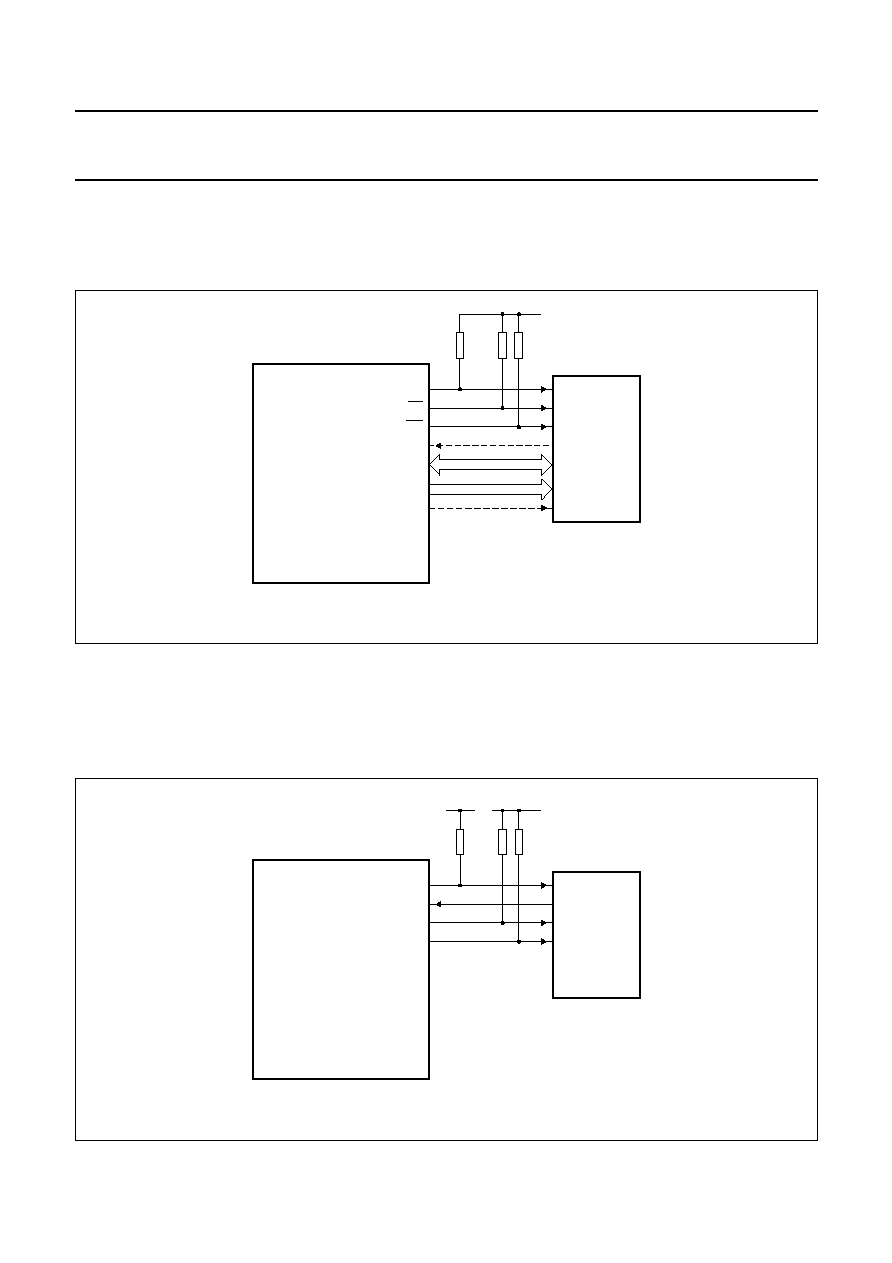
2001 Apr 17
57
Philips Semiconductors
Product specification
Digital telephone answering machine chip
PCD6001
12.1.1
DTAM
EXTERNAL MEMORY USING A PARALLEL FLASH
A parallel flash memory can be connected to the PCD6001 chip as shown in Fig.23. The MAGP and P2GP bits in the
XRAM-mapped Configuration Register (ConfReg) must be set. Clearing P4.3 will enable the flash memory.
12.1.2
DTAM
EXTERNAL MEMORY INTERFACE USING A
4-
WIRE SERIAL FLASH
A 4-wire serial flash memory (like SPI or Microwire flash memory) can be connected to the PCD6001 chip as shown in
Fig.24. P4.3 must be level shifted when using a 5 V serial flash memory. P4.1 and P4.2 must be pulled to 3 V with a
resistor. When using a 5 V flash memory the DO output of the flash must be level-shifted to 3 V with 2 resistors
(1 and 1.5 k
).
handbook, full pagewidth
MGT437
1 k
P4.3
1 k
CEN
RD
OEN
WR
WN
RY/BYN
P3.x
P1.x
P2, MA7 to MA0 and P4.0 to P4.2
VDD3V
P0
IO7 to IO0
A18 to A0
A19
PCD6001
4/8 MBIT
FLASH
Fig.23 Parallel flash memory connection.
handbook, full pagewidth
MGT438
1 k
P4.3
1 k
CEN
P4.4/FSI
DO
P4.2/FSO
DI
SK
P4.1/FSK
VDD3V
VDD3V/VDD5V
PCD6001
SERIAL
FLASH
Fig.24 Serial flash memory connection.
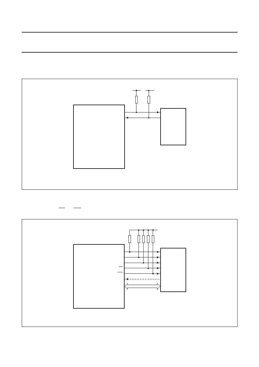
2001 Apr 17
58
Philips Semiconductors
Product specification
Digital telephone answering machine chip
PCD6001
12.1.3
DTAM
EXTERNAL MEMORY INTERFACE USING AN
I
2
C-
BUS SERIAL FLASH
An I
2
C-bus flash memory can be connected to the PCD6001 chip as shown in Fig.25.
handbook, full pagewidth
MGT439
1 k
P1.6/SCL
1 k
SCL
P1.7/SDA
SDA
VDD3V
VDD3V
PCD6001
I
2
C-BUS
FLASH
Fig.25 I
2
C-bus serial flash memory connection.
12.1.4
DTAM
EXTERNAL MEMORY USING A
CAD
FLASH
A CAD flash memory can be connected to the PCD6001 chip as shown in Fig.26. P4.3 must be pulled up to 3 V with a
resistor. P4.1, P4.2, RD and WR must also be pulled to 3 V with a resistor.
handbook, full pagewidth
MGT440
1 k
P4.3
1 k
CEN
P4.x
CLE
P4.y
ALE
RD
REN
WR
WEN
P1.x
RY/BYN
VDD3V
P0
IO7 to IO0
PCD6001
MUX
CAD
FLASH
Fig.26 Mixed CAD flash memory connection.

2001 Apr 17
59
Philips Semiconductors
Product specification
Digital telephone answering machine chip
PCD6001
12.1.5
DTAM
EXTERNAL MEMORY USING
DRAM
OR
ARAM
A standard DRAM or ARAM memory can be connected to the PCD6001 chip as shown in Fig.27. When WR/RD are not
programmed as push-pull outputs, a 1 k
pull-up resistor has to be connected to V
DD3V
.
handbook, full pagewidth
MGT441
WE
OE
CASN
D[3:0]
A[11:0]
RASN
WR
RD
P3.x
P0[3:0]
MA[7:0]
P2[3:0]
P3.y
PCD6001
ARAM
DRAM
Fig.27 DRAM/ARAM memory connection.
12.2
DTAM external interface during target
debugging
If the DTAM chip is used with the tScope-51 target debug
tool the DTAM chip needs executable SRAM where the
monitor program MON51 can store the program code. This
SRAM is accessible by means of the RD, WR and PSEN
signals. Since connection to parallel flash memory with
XSRAM and ROM is the worst case situation this case is
shown in Fig.28. Since it is not a commercial system
additional logic can be connected to the DTAM chip to
create executable SRAM.
The target debug logic only consists of combinational
logic:
∑
CENROM
P2.7, P2.6 or P2.5
∑
CENFLASH
P4.3
∑
CENXSRAM
(PSEN or not CENROM) and (RD or
not CENFLASH)
∑
OENXSRAM
PSEN and RD
∑
WRXSRAM
WR.
The port restore logic is necessary to make the MA/P2/P0
ports available for the application.
The MON51 program is assumed to be in the lowest
8 kbytes of the ROM. If the flash memory should be
accessed clear P4.3 to logic 0. Now the MON51 program
has no access to the XSRAM with RD so no breakpoints
are allowed in the code area where P4.3 is logic 0. Set
P4.3 to logic 1 again after the flash memory access to
enable MON51 again to access the XSRAM.
Target debugging requires I
2
C-bus and one general
purpose input port. This means that at least 31 I/O ports
are available for the application (not using parallel flash)
during target debugging.
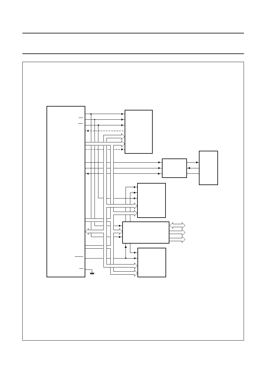
2001 Apr 17
60
Philips Semiconductors
Product specification
Digital telephone answering machine chip
PCD6001
handbook, full pagewidth
MGT443
P4.3
CEN
RD
OEN
WR
WN
RY/BYN
P3.x
P3.z
P1.x
P4.0 to P4.2
P1.6/SCL
P1.7/SDA
P0
P2
EA
PSEN
MA
IO7 to IO0
A18 to A0
A19
DACKN
SCL
SDA
PCD6001
4/8-Mbit
FLASH
KEIL
tScope-51
PC
CEN
P0_R
MA_R
P2_R
TX
RX
GND
OEN
WN
IO7 to IO0
A15 to A0
64-kbyte
XSRAM
CEN
OEN
IO7 to IO0
A15 to A0
MON51
ROM
TARGET DEBUG LOGIC
AND
OTP PORT RESTORE
I
2
C-BUS TO
RS232
CONVERTER
Fig.28 Flash, XSRAM and MON51 ROM memory connection.

2001 Apr 17
61
Philips Semiconductors
Product specification
Digital telephone answering machine chip
PCD6001
13 THE CODECs
13.1
Definitions
In the description of the CODECs, amplitude units in dB
are used. The following definitions apply:
∑
dBm: used for absolute analog signal power levels.
0 dBm equals 1 mW power dissipation in 600
. A
single sinewave signal with a power level of 0 dBm
corresponds to an RMS voltage value of 774.6 mV.
∑
dBmp: used for absolute analog signal power levels
with psophometric weighting according to
"CCITT
Recommendation G.223". This unit is used to express
analog noise power levels.
∑
dBm0: used for relative digital signal power levels.
0 dBm0 is defined in
"CCITT Recommendation G.711
(Section 4, Table 5)". It follows that the maximum digital
signal power level is 3.14 dBm0 (A-law). Thus
3.14 dBm0 is the RMS value of a sinewave signal whose
peaks just reach the full-scale of the digital code. For the
(internal) bitstream signal (output of ARS and DNS) the
positive full-scale value is a continuous stream of `ones',
whereas the negative full-scale value is a continuous
stream of `zeroes'. For the (internal) digital 14 or 16-bit
words, represented in 2s complement (MSB first) the
positive full-scale value is a `zero' followed by 13 or 15
`ones', whereas the negative full-scale value is a `one'
followed by 13 or 15 `zeroes'.
∑
dBm0p: used for relative digital signal power levels with
psophometric weighting according to
"CCITT
Recommendation G.223".
∑
dB: is used for the signal level gain between any two
nodes within the speech path. As different signal
representations are used within the speech path, the
gain value depends on the used signal definitions.
∑
dBp: is used for the signal level gain between any two
nodes within the speech path with psophometric
weighting according to
"CCITT Recommendation
G.223".
∑
The uniform PCM reference point is the (virtual) signal
node in the DSP at the input of the PCM encoder for the
analog-to-digital speech path and the output of the PCM
decoder for the digital-to-analog speech path.
13.2
CODEC architecture
The PCD6001 is provided with two CODECs that perform
the analog-to-digital and digital-to-analog conversion of
speech signals. In Fig.29, the CODECs are the interface
between the external analog peripherals and the DSP.
CODEC1 is used for the line interface and CODEC2 is
used for the loudspeaker and the microphone.
The DTCON register bit DTCON.4 selects the input to
CODEC1 (LIFMIN1 or LIFMIN2).
The main CODEC functions are (refer to Fig.29):
∑
AMP - Pre-amplifier
∑
ARS - Analog Receive Sigma delta ADC
∑
DDF - Digital Decimation Filter
∑
DNS - Digital Noise Shaper
∑
ATD - Analog Transmit DAC.
For CODEC1 the balanced line interface input is fed to the
ARS block that performs analog-to-digital conversion, the
gain of the input can be set to the amplification steps:
7, 23 and 35 dB (see Section 17.5 for typical/maximum
gain specifications). This programmable range is used by
the microcontroller on command of the DSP to perform
limit or automatic gain control. The analog data is
converted by ARS to a bit stream. The basic sampling
frequency (f
s
) is 8 kHz. The DDF decimates the bit stream
down to 16-bit linear PCM data. The DF has a gain of
3.14 dB (which has to be added to the programmable ARS
gain) to achieve a uniform reference point at the DSP input
for linear PCM data. Finally, the DSP will decimate this
data to 16-bit linear PCM data at a rate of 8 kHz.
The reverse operation is performed in the transmit path.
The DSP produces 16-bit linear PCM to the DNS. The ATD
which is a DAC converts the bit stream into an analog
signal. The converter has a programmable amplification
range of 18 dB. This programmability is
-
12,
-
6, +0 and
+6 dB.
CODEC2 is built-up in a similar manner as CODEC1, the
only difference being the microphone amplifier before the
ADC. This will amplify the balanced analog (microphone)
signal in the receive path with a fixed +15 dB (see
Section 17.5 for exact gain specifications). For direct
connectivity of an external microphone, a software on/off
switchable supply voltage is available.
Several registers are available for the CODECS control:
∑
DTCON: for selecting the input to CODEC1
(DTCON.4 = 0 means LIFMIN1 is selected,
DTCON.4 = 1 means LIFMIN2 is selected) and for
alternative gain settings (see Section 13.2.2)
∑
CDVC1: the volume control register for CODEC1
∑
CDVC2: the volume control register for CODEC2.
∑
CDTRx: test mode control registers for both CODECS
∑
PMTRx: test mode control registers for both CODECS

2001 Apr 17
62
Philips Semiconductors
Product specification
Digital telephone answering machine chip
PCD6001
13.2.1
V
OLUME
C
ONTROL
R
EGISTERS
(CDVC1
AND
CDVC2)
The Volume Control Registers are identical and both are reset to 00H. Table 54 is relevant to both registers.
Table 53 Volume Control Register 1 (SFR address BBH); Volume Control Register 2 (SFR address BCH)
Table 54 Digital-to-analog gain values
Note
1. In these gain values the
-
4 dB digital gain (software DSP output port gain of
-
2 dB and DNS path gain of
-
2 dB) is
not included as in previous PCD600x data sheets.
13.2.2
D
ATA
C
ONTROL
R
EGISTER
(DTCON)
Table 55 Data Control Register (SFR address C7H), reset state 00H
Table 56 Analog-to-digital gain values
Notes
1. The 3.14 dB digital gain of DDF hardware block is not included here. The nominal values given in this table are
rounded for naming convention. See Section 17.5 for exact typical/maximum gain specifications.
2. System application should be such that the maximum line input signal level does not exceed the specified value to
avoid distortion (see Section 17.5 for maximum input level specifications). At a maximum line input level of
-
37 dBm
full-scale control the internal ADC can still be achieved by a maximum gain setting of 35 dB.
3. System application should be such that the maximum differential microphone input signal level does not exceed the
specified value to avoid distortion (see Section 17.5 for maximum input level specifications). At a maximum
microphone input level of
-
52 dBm full-scale control the internal ADC can still be achieved by a maximum gain setting
of 50 dB. The high dynamic range of the ADC allows for additional digital gain up to 30 dB by the DSP.
4. If the HI_GAIN1/LO_GAIN2 bit is set to logic 1, the value of bit 3 of CDVC1/2 and AMP_EN is overruled and the gain
will be +35 dB for CODEC1 and +7 dB for CODEC2.
7
6
5
4
3
2
1
0
D/A.1
D/A.0
spare
spare
A/D
spare
spare
spare
CDVC1[7:4]/CDVC2[7:4]
DIGITAL-TO-ANALOG GAIN FOR CODEC1 AND CODEC2
(1)
00XX
-
12 dB
01XX
-
6 dB
10XX
0 dB
11XX
+6 dB
7
6
5
4
3
2
1
0
spare
spare
HI_GAIN1
LINESEL
spare
AMP_ENA
LO_GAIN2
spare
CODEC1 analog-to-digital gain and channel selection
CODEC2 analog-to-digital gain
CDVC1[3:0]/CDVC2
[3:0]
ANALOG-TO-DIGITAL GAIN
(1)
CODEC1 (LINE)
(2)
CODEC2 (MIC)
(3)
HI_GAIN1 (LINE)/LO_GAIN2 (MIC)
AMP_ENA = 0 AMP_ENA = 1
0XXX
7 dB
23 dB
38 dB
HI_GAIN1/LO_GAIN2 = 0
(4)
1XXX
23 dB
35 dB
50 dB
XXXX
35 dB
7 dB
HI_GAIN1/LO_GAIN2 = 1
(4)
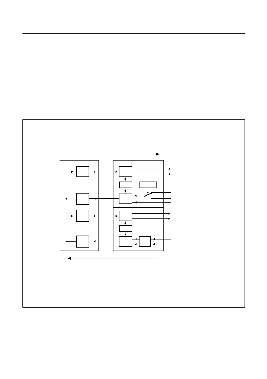
2001 Apr 17
63
Philips Semiconductors
Product specification
Digital telephone answering machine chip
PCD6001
The analog and digital parts of both CODECs can be
independently activated by the SYMOD register; see
Section 9.2.2. Bit 4 of SYMOD is used to activate the
microphone supply voltage, if the bit is logic 0 the supply is
off.
The balanced microphone input has a minimum differential
input resistance of R
MICDM
, and the balanced line interface
input has a minimum differential input resistance of
R
LIFINDM
.
The output resistance of the balanced CODEC outputs is
R
LIFOUT
for CODEC1 and R
SPKR
for CODEC2 at a
differential output level of 1350 mV (RMS). For exact
measurement conditions and specified values see
Section 17.5.
handbook, full pagewidth
MGT442
DTCON.4
CDVC1
ARS1
ATD1
DDF1
DNS1
DT1
DR1
LIFMOUT
line interface
output
line interface
input
loudspeaker
output
microphone
input
receive path
LIFPOUT
LIFMIN1
LIFMIN2
LIFPIN
CDVC2
ARS2
AMP
ATD2
DDF2
DNS2
DT2
DR2
transmit path
MICP
MICM
SPKRP
SPKRM
CODEC1
CODEC2
DSP
Fig.29 Block diagram of CODECs.

2001 Apr 17
64
Philips Semiconductors
Product specification
Digital telephone answering machine chip
PCD6001
14 ANALOG VOLTAGE REFERENCE (AVR)
14.1
Bandgap reference
The Analog Voltage Reference circuitry (AVR) includes a
bandgap circuit with a nominal output voltage of about
1.25 V. This voltage is used by the power-on reset block
and by the analog voltage source to generate the
reference voltage V
REF
.
Block AVR is always on, even in System-off mode, and will
consume only a few
µ
A of current. The output of AVR is
directly connected to the power-on reset block and it
determines the power-on reset threshold levels accuracy
in first order. The connection from AVR to the analog
voltage source circuitry (AVS, see Section 14.2) is via an
internal series resistor of about 500 k
(typical). The
voltage after this resistor is connected to pin V
BGP
, which
allows an external capacitor (100 nF) to be connected to
filter out any noise from AVR otherwise entering AVS.
With this configuration the noise at pin V
BGP
will be about
-
115 dBmp. The pin also allows a direct measurement of
the bandgap voltage, but no current must be drawn.
In order to guarantee a correct start-up of the bandgap
voltage under all conditions, a supply voltage ramp test is
performed on each device. The bandgap voltage is
compared against specified values at the indicated times
(see Fig.30). The test setup intends to reflect the worst
case start-up conditions which may occur in an application
(for initial power-up and after short power drop). Note that
t
rise
is critical and should not be greater than indicated in a
given application. Other indicated times (t
settle
and t
rise
)
reflect the worst case conditions for the device and
therefore can change in the application.
handbook, full pagewidth
MGT445
tfall
tsettle
trise
t
measure VBGP
VDDA
0 V
0.6 V
2.5 V
tfall = 2 ms
tsettle = 45 ms
trise = 20 ms
Fig.30 Bandgap voltage test setup.

2001 Apr 17
65
Philips Semiconductors
Product specification
Digital telephone answering machine chip
PCD6001
14.2
Analog Voltage Source (AVS)
The analog voltage source generates the following
voltages:
∑
A precise reference voltage V
REF
. The value in register
VREFR determines the V
REF
. In the application this
voltage should be tuned to 2000 mV, since it will
determine the absolute accuracy of the auxiliary
analog-to-digital and digital-to-analog conversion. V
REF
is the direct output of an opamp which can source an
output current, and not sink. An external capacitor
should be connected between V
REF
and V
SSA
for
stability and noise performance. The reference voltage
can also directly supply an external electret microphone
via pin V
MIC
. The switch between V
REF
and V
MIC
is
controlled via bit 4 in the SYMOD special function
register.
∑
An analog output voltage DAOUT. This voltage can be
set between approximately 8 mV (1 LSB = V
REF
/256)
and V
REF
(= 2000 mV) by changing the contents of
register GPDAR. This large range is possible when no
opamp is used.
This causes a relatively high output resistance with a
settling time of about 10 ms. The dynamic switching of
DAOUT causes the output resistance to be dependent
of the actual load on DAOUT. This effect can be
cancelled if an external capacitor larger than 500 pF
between DAOUT and V
SSA
is applied. This will however
result in a slower settling time of the output voltage, to
about 30
µ
s.
∑
The internal analog common mode voltage V
acm
, used
in the CODEC.
∑
The internal voltage V
adc
is used only when an
analog-to-digital conversion is executed.
As mentioned above, for highest analog performance the
reference voltage V
REF
has to be adjusted in the
application to 2000 mV. For this purpose the VREFR SFR
has been defined. The reset state should ensure that the
reference voltage is about 2000 mV on a typical device.
Exact adjustment has to be done under software control
using the VREFR register, where increasing the V
REFR
value will decrease the reference voltage.
14.2.1
V
OLTAGE
R
EFERENCE
R
EGISTER
(VREFR)
Table 57 Voltage Reference Register (SFR address BAH); reset state A0H
7
6
5
4
3
2
1
0
VREF.7
VREF.6
VREF.5
VREF.4
VREF.3
VREF.2
VREF.1
VREF.0

2001 Apr 17
66
Philips Semiconductors
Product specification
Digital telephone answering machine chip
PCD6001
15 IOM
15.1
Features
The IOM block in the PCD6001 is a 4-wire serial interface
performing following functions:
∑
Digital interface with up to two 64 kbits/s channels at a
bit rate of n
◊
256 kbits/s (n = 1, 2, 3, 4 or 8), complying
with the
"IOM-2 specifications" (IOM-2 is a registered
trademark of Siemens AG)
∑
Digital interface with 32 slots/frame and non-doubled
data clock; compatible with the digital interface of some
speech CODEC ICs
∑
Autonomous storing/fetching of data into/from the
DSP I/O registers
∑
Byte or word (16 bits) transfer.
15.2
Pin description
The following pins are used by the IOM interface:
∑
DI: serial data input with a bit rate of n
◊
256 kbits/s
(n = 1, 2, 3, 4 or 8)
∑
DO: serial data output with a bit rate of n
◊
256 kbits/s
(n = 1, 2, 3, 4 or 8)
∑
FSC: 8 kHz frame synchronization input/output
∑
DCK: data clock input/output. Twice the data
transmission frequency on DI and DO, except in the
non-doubled data clock mode (see Section 15.3).
These pins are alternative functions of P3. When
activated, DO is an open-drain pin, as many devices must
be able to write on the same data line in a time-multiplexed
mode. Therefore DO must be externally pulled-up. FSC
and DCK are inputs or push-pull outputs, depending on the
IOM being in Slave or Master mode. Activation of the IOM
alternative functions of P3 and switching between Slave or
Master mode is controlled by the SFR ALTP, bit 6 and 5
respectively (see Section 16.2 for more details).
15.3
Functional description
The digital interface of the PCD6001 can work at several
bit rates, summarized in Table 61. A particular bit rate is
selected by writing the 3-bit code given in the first column
of the table into the IOM control register bits IOMC[15:13].
Choosing the code `000' or `001' deactivates the IOM
interface and stops all the transactions on the IOM bus.
This is the default state after reset.
The PCD6001 IOM can be master or slave. After reset the
IOM is in Slave mode. Switching between Slave or Master
mode is controlled by the SFR ALTP, bit 6 and bit 5
respectively (see Section 16.2.5 for more details). In Slave
mode both FSC and DCK are inputs. In Master mode both
FSC and DCK are outputs. In Master mode FSC and DCK
are generated by the TICB (see Section 9.1). Master mode
should only be used in combination with the bit rate
768 kbits/s. Slave mode should only be used when
operating with a 3.456 MHz (or multiple) crystal. In
general, proper IOM functionality is only guaranteed
at DSP operating frequencies of 28 and 42 MHz.
FSC is an 8 kHz framing signal for synchronizing data
transmission on DI and DO. The rising edge of FSC gives
the time reference for the first bit transmitted in the first slot
of a speech frame. The number of slots per speech frame
depends on the selected data rate. Each slot contains
8 data bits.
DCK is a data clock. Its frequency is twice the selected
data rate in IOM mode. In speech mode, the
DCK frequency is equal to the data rate (2048 kHz for
2048 kbits/s).
DI is the serial data input. Data coming on DI in packets of
8 bits (A-law PCM encoded data) or 16 bits (linear PCM
data) is stored temporarily in an IOM data buffer, from
where it is processed by the on-chip DSP. On the other
hand, data written into the IOM data buffers by the DSP is
shifted out on pin DO.
There are two IOM data buffers, allowing the use of two
8-bit channel. One channel is 64 kbits/s in case of A-law
PCM encoded data and 128 kbits/s if linear PCM data is
transferred, in which case two consecutive slots are used.
The speech mode was implemented to support the Codec
interface of some speech compression ICs. This mode is
very similar to the IOM 32 slots mode, the main difference
being the non-doubled data clock. See Section 15.6 for
timing information.
15.4
IOM data buffers
Table 58 and 59 show the two 16-bit DSP registers used
as data buffers: IOMDI for storing inbound data and
IOMDO for the outbound data. The high bytes store the
data of buffer 1, the low bytes the data of buffer 0.

2001 Apr 17
67
Philips Semiconductors
Product specification
Digital telephone answering machine chip
PCD6001
15.4.1
IOM D
ATA
I
N
R
EGISTER
(IOMDI)
Table 58 IOM Data In Register; reset state 00H
15.4.2
IOM D
ATA
O
UT
R
EGISTER
(IOMDO)
Table 59 IOM Data Out Register; reset state 00H
15.5
IOM Control Register (IOMC)
The bit rates, the selection of active slots on the IOM interface and the logic connection between an IOM slot and an IOM
data buffer are defined in the IOM Control Register. The IOM modes which can be selected are listed in Table 61.
Writing to the IOMC register is done via the Application Programming Interface (API) software. Please refer to the API
specification for more details.
Table 60 IOM Control Register; reset state 00H
Table 61 Selection of IOM modes
Note
1. The Speech mode is similar to the IOM slave 32 slots mode, but with a non-doubled data clock DCK.
15
14
13
12
11
10
9
8
7
6
5
4
3
2
1
0
IOM inbound data buffer 1
IOM inbound data buffer 0
15
14
13
12
11
10
9
8
7
6
5
4
3
2
1
0
IOM outbound data buffer 1
IOM outbound data buffer 0
15
14
13
12
11
10
9
8
7
6
5
4
3
2
1
0
IOM Mode select
IOM buffer 0; slot position
spare
buffer 0
active
buffer 1
active
IOM buffer 1; slot position
IOMC[15:13]
MODE
000 or 001
Inactive (default after reset)
010
IOM Slave mode, 256 kbits/s in 4 slots/speech-frame
011
IOM Slave mode, 512 kbits/s in 8 slots/speech-frame
100
IOM Master/Slave mode, 768 kbits/s in 12 slots/speech-frame
101
IOM Slave mode, 1024 kbits/s in 16 slots/speech-frame
110
Speech Slave mode, 2048 kbits/s in 32 slots/speech-frame
(1)
111
IOM Slave mode, 2048 kbits/s in 32 slots/speech-frame

2001 Apr 17
68
Philips Semiconductors
Product specification
Digital telephone answering machine chip
PCD6001
15.6
Timing
The timing on the 4-wire interface is given in Fig.31 and Table 62 for the IOM mode and in Fig.32 and Table 63 for the
speech mode.
handbook, full pagewidth
MGM794
DCK
FSC
DI/DO
DCK
FSC
DO
DI
bit 7
bit 6
bit 5
tr(DCK)
tf(DCK)
td(F)
tWH
td(DF)
td(DC)
tsu(F)
th(D)
tsu(D)
tw(FH)
tWL
TDCK
bit 7
bit 7
Fig.31 4-wire interface timing in IOM mode.
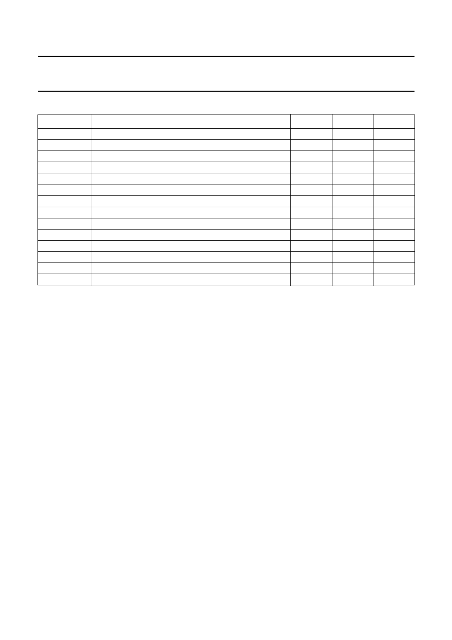
2001 Apr 17
69
Philips Semiconductors
Product specification
Digital telephone answering machine chip
PCD6001
Table 62 Timing parameters in IOM mode
Notes
1. Corresponds to the highest DCK frequency allowed (4.096 MHz) with a 10% margin.
2. Condition C
L
= 150 pF.
SYMBOL
PARAMETER
MIN.
MAX.
UNITS
t
r(DCK)
data clock rise time
-
60
ns
t
f(DCK)
data clock fall time
-
60
ns
T
DCK
data clock period
220
(1)
-
ns
t
WH
data clock HIGH time pulse width
80
-
ns
t
WL
data clock LOW time pulse width
80
-
ns
t
r(FSC)
frame sync rise time
-
60
ns
t
f(FSC)
frame sync fall time
-
60
ns
t
d(FSC)
frame sync delay time
-
t
WL
60
ns
t
su(FSC)
frame sync set-up time
60
-
ns
t
WFH
frame sync HIGH time pulse width
130
-
ns
t
d(DC)
output data to data clock delay time
-
100
(2)
ns
t
d(DF)
output data to frame sync delay time
-
150
(2)
ns
t
su(D)
input data set-up time
t
WH
-
ns
t
h(D)
input data hold time
50
-
ns
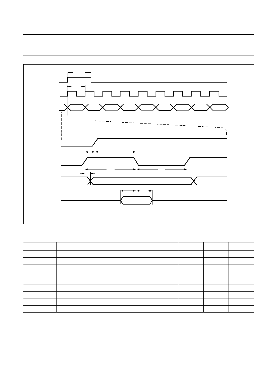
2001 Apr 17
70
Philips Semiconductors
Product specification
Digital telephone answering machine chip
PCD6001
Table 63 Timing parameters in speech mode
Notes
1. Corresponds to the DCK frequency (2.048 MHz) with a 10% margin.
2. Condition C
L
= 150 pF.
SYMBOL
PARAMETER
MIN.
MAX.
UNITS
t
d(FSC)
frame sync (FSC) delay time
-
t
WL
100
ns
t
su(FSC)
frame sync (FSC) set-up time
60
-
ns
t
WFH
frame sync (FSC) high time pulse width
130
-
ns
T
DCK
data clock (DCK) period
440
(1)
-
ns
t
WH
data clock (DCK) high time pulse width
150
-
ns
t
WL
data clock (DCK) low time pulse width
150
-
ns
t
d(DC)
output data (DO) to data clock delay time
-
100
(2)
ns
t
su(D)
input data (DI) set-up time
60
-
ns
t
h(D)
input data (DI) hold time
60
-
ns
handbook, full pagewidth
FSC
DCK
DI/DO
FSC
DCK
DO
B7
B7
B6
DI
B2
B1
B0
B5
B4
B3
B6
B7
tW(FH)
TDCK
tsu(FSC)
th(D)
tsu(D)
tWH
tWL
td(FSC)
td(DC)
MGM795
Fig.32 4-wire interface timing in speech mode.
2001 Apr 17
71
Philips Semiconductors
Product specification
Digital telephone answering machine chip
PCD6001
16 EXTERNAL I/O INTERFACES
16.1
External analog interfaces
16.1.1
G
ENERAL PURPOSE
ADC
AND
DAC
For general use, for instance battery management, parallel
set detection or speaker amplifier volume control, a 2-line
multiplexed 8-bit ADC and an 8-bit DAC are on-chip. The
ADC and the DAC consist of several analog sub-blocks
called AVS and AAD, which are controlled by the digital
block DCA (see Fig.33). Block AVS generates voltages in
a time multiplexed way, and acts as a DAC with the
bandgap voltage V
BGP
as input voltage. Block AAD
contains a comparator that is part of the successive
approximation ADC formed by a combination of AVS, AAD
and DCA. The analog-to-digital conversion can be
performed on two external input signals: AD0IN and
AD1IN.
The whole circuit is active as long as the chip is in
System-on mode. Both the ADC and the DAC can be
controlled by the microcontroller, the SFR mapped
DCA block allowing the user a flexible interface to analog
peripherals.
16.1.2
G
ENERAL PURPOSE
ADC
The on-chip ADC is a two channel multiplexed 8-bit
converter. The control of this converter is done via two bits
in the microcontroller GPADC SFR. One bit selects the
channel and the other bit is the converter request bit. The
request bit is reset by hardware when the converter has
finished its conversion cycle. The ADC (AAD in Fig.33), is
of the successive approximation type.
An internal register contains the value of the slider position
and is changed after each comparison of V
adc
with one of
the two possible analog-to-digital inputs (AD0IN and
AD1IN). After 8 comparisons the conversion is finished
and the contents of the internal register is copied into the
register GPADR. Total analog-to-digital conversion time
(from setting the Request bit until GPADR ready) is less
than 50 ms. This register can in turn be read by the internal
microcontroller.
16.1.2.1
General Purpose ADC Register (GPADC)
Table 64 General Purpose ADC Register (SFR address C3H); reset state 00H
Table 65 Description of GPADC bits
16.1.2.2
General Purpose ADC Result Register (GPADR)
This register holds the 8-bit result value from the conversion. The conversion range is 0 to 2000 mV (V
REF
) with 8 mV
resolution.
Table 66 General Purpose ADC Result Register (SFR address C2H); reset state 00H, read only
7
6
5
4
3
2
1
0
-
-
-
-
-
AADC
CS
REQCOM
BIT
SYMBOL
DESCRIPTION
7 to 3
-
These 5 bits are reserved.
2
AADC
Automatic Analog-to-Digital Conversion. If AADC = 1, then a conversion is
performed every 30 ms, regardless of state of request confirm bit.
1
CS
Channel Select. If CS = 0, analog-to-digital conversion input is on pin AD0IN. If CS = 1,
analog-to-digital conversion input is on pin AD1IN. Switching of the analog-to-digital
channel is only allowed when no analog-to-digital conversion currently is in progress.
Otherwise the resulting value will be corrupt.
0
REQCOM
Request Confirm.
7
6
5
4
3
2
1
0
A/D.7
A/D.6
A/D.5
A/D.4
A/D.3
A/D.2
A/D.1
A/D.0

2001 Apr 17
72
Philips Semiconductors
Product specification
Digital telephone answering machine chip
PCD6001
16.1.3
G
ENERAL PURPOSE
DAC
The on-chip DAC is a single channel 8-bit converter. The control of this converter is done via the GPDAR register. The
value written in this register triggers the conversion which will be present at the output pin after the digital-to-analog
conversion cycle (<25
µ
s). The range from the digital-to-analog output is 0 to 2000 mV (V
REF
).
The conversion principle for both analog-to-digital and digital-to-analog conversion is shown in Fig.34.
16.1.3.1
General Purpose DAC Register (GPDAR)
Table 67 General Purpose DC A Register (SFR address C4H); reset state 80H
7
6
5
4
3
2
1
0
D/A.7
D/A.6
D/A.5
D/A.4
D/A.3
D/A.2
D/A.1
D/A.0
handbook, full pagewidth
MGM796
VACM
RDAC
VADC
AVS
AAD
SYMOD.4 (MIC supply bit)
VMIC
Vref
DAOUT
AD0IN
AD1IN
VREFR
DCA
GPADC
GPDAR
GPADR
GPADC
(channel
request bit)
VBGP
Fig.33 The architecture of the auxiliary DAC and ADC.
handbook, full pagewidth
MGM797
time
pin GPDAR
represents output
GPADC SFR
has been changed
by the microcontroller
GPADC SFR
has been changed
by the micro
HW resets request bit.
Conversion finished.
Result in GPADR SFR
conversion cycle (
<
30
µ
s)
analog-to-digital conversion
conversion cycle (
<
10
µ
s)
digital-to-analog conversion
Fig.34 Analog-to-digital and digital-to-analog conversion principle.
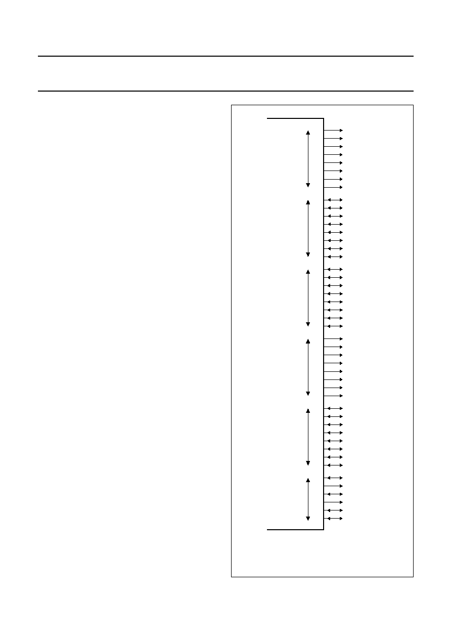
2001 Apr 17
73
Philips Semiconductors
Product specification
Digital telephone answering machine chip
PCD6001
16.2
External digital Interfaces
For control of peripherals like a display, ringer, key pad
and line interface a large number of general purpose
digital I/O pins are available in addition to the flash
memory, LCD control pins and MSK or IOM modem pins.
The exact number of free I/O pins depends on the choice
of peripherals that make up the system configuration. In
case all alternative port functions of P1 and P3 are used,
10 input lines remain available on P1 and P3 of which 7
are programmable for interrupts.
I/O ports P1 and P3 are `weak pull-up' types which can
therefore be used either as inputs or outputs. The reset
value of P1 and P3 is FFH (input mode). In output mode
for driving with a logic 1 (weak pull-up) the external load of
P1 and P3 should be equivalent to >100 k
, for `driving'
with a logic 0 the sink current should not exceed 4 mA.
In addition to P1 and P3 there are 16 output ports
available at P2 and MA. Output Ports P2 and MA are
push-pull ports and their reset value is 00H (output 00H).
The driving level of P2 and MA is 4 mA for either logic 0 or
logic 1. Port P4 provides the flash memory and display
control signals. The P1, P3 and P4 I/O lines are available
as SFR bit-addressable I/O registers in the configuration
shown in Fig.35, while P2 and MA are available as (not bit
addressable) XDATA mapped ports (for exact
configuration and detailed description see Chapter 12).
The MA and P2 ports are described in Chapter 12. The
configuration of Ports P1 and P3 are described in the
Tables 68 to 76.
MGM798
MA0
0
MA1
1
MA2
2
MA3
3
MA4
4
MA5
5
MA6
6
MA7
7
MA
P00
0
P01
1
P02
2
P03
3
P04
4
P05
5
P06
6
P07
7
P0
P1.0/EX2
0
P1.1/EX3
1
P1.2/EX4
2
P1.3/EX5
3
P1.4/EX6
4
P1.5
5
P1.6/SCL
6
P1.7/SDA
7
P1
P2.0
0
P2.1
1
P2.2
2
P2.3
3
P2.4
4
P2.5
5
P2.6
6
P2.7
7
P2
P3.0/MOUT0/DO
0
P3.1/MOUT1/DCK
1
P3.2/EX0N
2
P3.3/EX1N
3
P3.4/T0
4
P3.5/T1
5
P3.6/MOUT2/FSC
6
P3.7/MIN/DI
7
P3
P4.0/LE
0
P4.1/FSK
1
P4.2/FSO
2
P4.3
3
P4.4/FSI
4
P4.5/GPC
5
P4
Fig.35 DTAM general purpose digital I/O
configuration.
2001 Apr 17
74
Philips Semiconductors
Product specification
Digital telephone answering machine chip
PCD6001
16.2.1
P
ORT
1 R
EGISTER
(P1)
The alternative outputs (SDA and SCL) are connected with the general purpose outputs via an AND logic gate. Therefore
when using the alternative functions the corresponding port bits have to be set to a logic 1.
For control of I
2
C-bus peripherals like for instance EEPROMs and LCD displays, P1.6 and P1.7 can also be used as SDA
and SCL to support I
2
C-bus. See Section 10.11 on how to activate this alternative function of P1.6 and P1.7. The rest of
Port 1 is defined as general purpose I/O pins as for the standard 80C51 microcontroller.
Table 68 Port 1 Register (SFR address 90H); bit addressable; reset state FFH
Table 69 P1 pin configuration
16.2.2
P
ORT
3 R
EGISTER
(P3)
Port 3 is defined as a set of 8 general purpose I/O pins similar to the standard 80C51 microcontroller except for P3.6 and
P3.7 which do not have the RD and WR functionality (the RD and WR are separate pins). Table 72 gives the different
functions and the corresponding port configurations available on P3.7, P3.6, P3.1 and P3.0. The last column gives the
function and configuration after reset.
Table 70 P3 (B0H) bit assignment; bit addressable; reset state FFH; note 1
Note
1. The alternative outputs (for MSK, IOM) are connected with the general purpose outputs via an AND logic gate.
Therefore when using the alternative functions the corresponding port bits have to be set to a logic 1.
Table 71 P3 pin configuration
Table 72 Port 3.7, 3.6, 3.1 and 3.0 modes and configuration
7
6
5
4
3
2
1
0
P1.7/SDA
P1.6/SCL
P1.5
P1.4/EX6
P1.3/EX5
P1.2/EX4
P1.1/EX3
P1.0/EX2
PORT PINS
CONFIGURATION
P1.7 and P1.6
open-drain
P1.5 to P1.0
quasi-bidirectional
7
6
5
4
3
2
1
0
P3.7/MIN/DI
P3.6/MOUT
2/FSC
P3.5/T1
P3.4/T0
P3.3/EX1N
P3.2/EX0N
P3.1/MOUT
1/DCK
P3.0/MOUT
0/DO
PORT PINS
CONFIGURATION
P3.7, P3.6, P3.1 and P3.0
see Table 72
P3.5 to P3.2
quasi-bidirectional
MSK
IOM
GENERAL PURPOSE I/O PORT
(RESET STATE)
SIGNAL
MASTER
SLAVE
MOUT0
push-pull
DO
open-drain 4 mA
open-drain 4 mA
P3.0
quasi-bidirectional
weak pull-up
MOUT1
push-pull
DCK
push-pull
input
P3.1
MOUT2
push-pull
FSC
push-pull
input
P3.6
MIN
input
DI
input
input
P3.7

2001 Apr 17
75
Philips Semiconductors
Product specification
Digital telephone answering machine chip
PCD6001
16.2.3
P
ORT
4 R
EGISTER
(P4)
The alternative outputs (GPC, FSO, FSK and LE) are connected with the general purpose outputs via an AND gate.
Therefore, when using the alternative functions the corresponding port bits should be set to a logic 1.
Table 73 Port 4 Register (SFR address 98H); bit addressable; reset state 1EHH; note 1
16.2.4
P
ORT
4 C
ONFIGURATION
R
EGISTER
(P4CFG)
This register is used to select the output configuration of the pins WR, RD and P4.0 to P4.4. The output configuration is
open-drain by default after reset. Note that the output configuration of P4.5 is selected by the P4.5 bit in SFR ALTP.
Table 74 Port 4 Configuration Register (SFR address 9FH); reset state 00H
Table 75 Description of P4CFG bits
16.2.5
A
LTERNATIVE
P
ORT
F
UNCTION
R
EGISTER
(ALTP)
This register selects the pin configuration for the MSK, IOM master/slave and general purpose function; see Table 77.
The general purpose clock function is described in Section 9.1. The LE functionality is described in Section 10.13.
Table 76 Alternative Port Function Register (SFR address ABH); reset state 00H
Table 77 P3.7, P3.6, P3.1 and P3.0 selection of pin configurations for alternative function
7
6
5
4
3
2
1
0
-
-
P4.5/GPC
P4.4/FSI
P4.3
P4.2/FSO
P4.1/FSK
P4.0/LE
7
6
5
4
3
2
1
0
WR
RD
EAM
P4.4
P4.3
P4.2
P4.1
P4.0
BIT
SYMBOL
DESCRIPTION
7
WR
If WR = 0, then open-drain configuration. If WR = 1, then push-pull configuration.
6
RD
If RD = 0, then open-drain configuration. If RD = 1, then push-pull configuration.
5
EAM
The EAM bit is used to select the Enhanced Addressing Mode; this is described in more
detail in Chapter 12.
4
P4.4
If P4.4 = 0, then open-drain configuration. If P4.4 = 1, then push-pull configuration.
3
P4.3
If P4.3 = 0, then open-drain configuration. If P4.3 = 1, then push-pull configuration.
2
P4.2
If P4.2 = 0, then open-drain configuration. If P4.2 = 1, then push-pull configuration.
1
P4.1
If P4.1 = 0, then open-drain configuration. If P4.1 = 1, then push-pull configuration.
0
P4.0
If P4.0 = 0, then open-drain configuration. If P4.0 = 1, then push-pull configuration.
7
6
5
4
3
2
1
0
-
IOM on P3
IOM master/
MSK
P4.5
GPC off/on
GPC source
LE off/on
early LE
ALTP.6
ALTP.5
MODE
0
0
general purpose I/O port
0
1
MSK
1
0
IOM slave
1
1
IOM master
2001 Apr 17
76
Philips Semiconductors
Product specification
Digital telephone answering machine chip
PCD6001
17 ELECTRICAL CHARACTERISTICS
17.1
Limiting values
In accordance with the Absolute Maximum Rating System (IEC 60134); note 1
Note
1. Parameters are valid over operating temperature range unless otherwise specified; all voltages are with respect to
V
SS
unless otherwise specified.
SYMBOL
PARAMETER
MIN.
MAX.
UNIT
V
DD3V
supply voltage 3.0 V (V
DD3V2
and V
DD3V3
)
-
0.5
+3.6
V
V
DD2.5V
supply voltage 2.5 V (V
DD3V1
, V
DDA
, V
DDPLL
)
-
0.5
+3.3
V
V
I
input voltage on any pin with respect to ground (V
SS
)
-
0.5
V
DD
+ 0.5
V
I
I/O
maximum sink/source current for all input/output pins
-
10
+10
mA
I
VDD
, I
VSS
maximum DC current for each supply pin
-
150
mA
P
tot
total power dissipation
-
800
mW
V
ESD(HBM)
maximum ESD stress level applied; according to human body
model (100 pF; 1.5 k
)
-
1500
V
V
ESD(MM)
maximum ESD stress level applied; according to machine model
(200 pF; 0.75
µ
H)
-
150
V
T
amb
operating ambient temperature
-
25
+70
∞
C
T
stg
storage temperature
-
65
+150
∞
C
2001 Apr 17
77
Philips Semiconductors
Product specification
Digital telephone answering machine chip
PCD6001
17.2
Supply characteristics
Notes
1. This defines requirements for the external Power-on reset circuit. The exact requirements can be relaxed depending
on the specific application. A hysteresis is required to overcome reset oscillations especially in battery operated
applications.
2. For these parameters, the recommended external components are specified which are supported by the internal
oscillator. This is not measured on a sample-by-sample basis.
SYMBOL
PARAMETER
CONDITIONS/REMARKS
MIN.
TYP.
MAX.
UNIT
V
DD3V1
digital supply voltage to pins
V
DD3V1
2.25
2.5
2.75
V
V
DD3V2/3
digital supply voltage to pins
V
DD3V2
and V
DD3V3
voltage must be set equal or higher
than V
DD3V1
2.25
3.0
3.3
V
V
DDA
analog supply voltage to pin
V
DDA
2.25
2.5
2.75
V
V
DDPLL
analog supply voltage to pin
V
DDPLL
2.25
2.5
2.75
V
I
DD(max)
total input current when
recording a message from
PSTN, CAS, line echo
cancellation, listen in on
CODEC2 to all supply pins
PLL on; CODEC1 and CODEC2
active; DSP at 42 MHz; microcontroller
at 21 MHz;
V
DD3V1
= V
DDA
= V
DDPLL
= 2.75 V;
V
DD3V2
= V
DD3V3
= 3.30 V; no load
-
28
35
mA
V
DD3V1
only
-
22.0
-
mA
V
DD3V2
only
no load on port pins
-
0.01
-
mA
V
DD3V3
only
no load on port pins
-
0.01
-
mA
V
DDA
only
-
5.0
-
mA
V
DDPLL
only
-
0.5
-
mA
I
DD(POTS)
POTS mode supply current
to all supply pins
PLL off; DSP only generating DTMF
tones; only CODEC1 D/A on;
microcontroller in power-down;
XTAL runs at 3.58 MHz; PMTR2.0 = 1;
CDTR2.0 = 1;
V
DD3Vx
= V
DDA
= V
DDPLL
= 2.25 V;
no load
-
2.6
3.5
mA
I
DD(sys-off)
total input current when in
System-off mode
digital-to-analog part of CODEC1 and
CODEC2 switched-off
-
0.17
0.90
mA
POR (Power-on reset)
V
th(H)
POR threshold value HIGH
note 1
-
-
2.2
V
V
th(L)
POR threshold value LOW
note 1
1.8
-
-
V
V
hys
POR hysteresis
note 1
0.08
-
-
V
OSC
C
L(xtal1,2)
crystal load capacitances at
XTAL1 and XTAL2 to V
SS
3.45 to 13.824 MHz; note 2
-
18
39
pF
R
S
crystal series resistance
3.58 MHz; note 2
-
-
300
13.824 MHz; note 2
-
-
40
C
P
crystal shunt capacitance
note 2
-
-
7
pF

2001 Apr 17
78
Philips Semiconductors
Product specification
Digital telephone answering machine chip
PCD6001
17.3
Digital I/O
Notes
1. V
DD(periph)
refers to the peripheral supplies V
DD3V2
and V
DD3V3
.
2. V
DD
-
VOUT = 400 mV (for I
OH
), VOUT
-
V
SS
= 400 mV (for
|
I
OL
|
).
3. 4 mA drive levels are only guaranteed for V
DD3V2/3
greater than 2.7 V.
4. On a LOW-to-HIGH transition, the output current value will be 4 mA for one microcontroller clock period, before
changing to the specified lower value. V
DD3Vx
= V
DDA
= V
DDPLL
= 2.75 V.
5. If the MSK mode is activated, the output current value for P3.0, P3.1 and P3.6 will continuously be 4 mA. If the IOM
Master mode is activated, the output current value for P3.1 and P3.6 will continuously be 4 mA.
6. When configured as push-pull.
SYMBOL
PARAMETER
CONDITIONS
MIN.
MAX.
UNIT
V
IL
LOW-level input voltage
SDA and SCL
0
0.3V
DD3V1
V
other pins
note 1
0
0.2V
DD(periph)
V
V
IH
HIGH-level input voltage
SDA and SCL
0.7V
DD3V1
V
DD(periph)
V
other pins
note 1
0.8V
DD(periph)
V
DD(periph)
V
|
I
OL
|
LOW-level output current
notes 2 and 3
RD, WR, PSEN, P0, P1, P2, P3,
P4 and MA
4
-
mA
I
OH
HIGH-level output current
notes 2 and 3
RD
(6)
, WR
(6)
, PSEN, P0, P2,
P4
(6)
and MA
-
mA
P1.0, P1.1, P1.2, P1.3, P1.4,
P1.5 and P3
90
(4)(5)
250
(4)(5)
µ
A
I
load
Total static load current on V
DD3V2
/V
DD3V3
-
30
mA
2001 Apr 17
79
Philips Semiconductors
Product specification
Digital telephone answering machine chip
PCD6001
17.4
Analog supplies and general purpose ADC and DAC
Notes
1. V
BGP
output current is zero. Decoupling capacitance between V
BGP
and V
SSA
is 100 nF.
2. The V
REF
output current is zero however the V
REF
output buffer is loaded via V
MIC
(see note 3). Decoupling
capacitance between V
REF
and V
SSA
is between 1 and 100
µ
F, with a 100 nF capacitance in parallel. The output can
only source current (i.e. not sink).
3. Pin V
MIC
is connected to V
REF
via an internal switch. The V
MIC
switch is closed by setting SYMOD.4 = 1. The V
MIC
DC output current is max. 400
µ
A, and V
REF
must be programmed to its typical value. For the connections of V
MIC
to
a microphone (see Fig.36). V
MIC
adjustment can only be done by adjusting V
REF
.
4. Output resistances represent the theoretical maximum which can be guaranteed by design. Actual output resistance
values can vary depending on several conditions as processing, temperature and drive signal shape.
SYMBOL
PARAMETER
CONDITIONS
MIN.
TYP.
MAX.
UNIT
V
BGP
AVR bandgap voltage
note 1
1.15
1.23
1.30
V
V
REF(RESET)
reference voltage, after reset
note 2
1.9
2.0
2.1
V
V
REF(TUNED)
reference voltage when tuned via
VREFR
-
30
-
mV
dV
MIC
V
REF
-
V
MIC
note 3
-
40
-
mV
V
ADIN,OFS
ADIN1 and ADIN2 input offset
voltage
-
20
50
mV
V
ADIN1,2
ADIN1 and ADIN2 input voltage
range
0
-
V
REF
mV
R
ADIN1,2
ADIN1 and ADIN2 input
resistance
2
10
-
M
R
DAOUT
DAOUT output resistance
note 4
-
7
-
k
V
DAOUT
DAOUT output voltage range
8
-
V
REF
mV
2001 Apr 17
80
Philips Semiconductors
Product specification
Digital telephone answering machine chip
PCD6001
17.5
CODECs
For all values specified, V
REF
is tuned to 2.0 V; unless mentioned differently, typical values for the analog-to-digital and
digital-to-analog filter characteristics conform to the G.712 specification.
SYMBOL
PARAMETER
CONDITIONS
MIN.
TYP.
MAX.
UNIT
Analog-to-digital path performance
V
MIC
maximum microphone input level
notes 1 and 2
-
-
-
8
dBm
R
MIC(DM)
microphone input resistance from
MICM to MICP, differential mode
notes 3 and 4
-
250
-
k
R
MIC(CM)
microphone input resistance from
MICM to V
SSA
or MICP to V
DDA
,
common mode
notes 3 and 5
-
25
-
k
V
LIFIN(max)
maximum line input level
notes 1 and 6
-
-
-
8
dBm
R
LIFIN1(dif)
line input resistance from LIFMIN1 to
LIFPIN, differential mode
notes 3 and 7
-
1000
-
k
R
LIFIN1(CM)
minimum line input resistance from
LIFMIN1 to VSSA or LIFPIN to V
DDA
,
common mode
notes 3 and 8
-
25
-
k
R
LIFIN2(dif)
minimum line input resistance from
LIFMIN2 to LIFPIN, differential mode
notes 3 and 9
-
50
-
k
R
LIFIN2(CM)
minimum line input resistance from
LIFMIN2 to V
SSA
, common mode
notes 3 and 10
-
1000
-
k
G
(A/D)(7dB)
typical analog-to-digital path gain of
CODEC1/ CODEC2 from LIF/MIC to
DR1/DR2
notes 1 and 11
-
7.1
-
dB
G
(A/D)(23dB)
notes 1 and 12
-
23.5
-
dB
G
(A/D)(35dB)
notes 1 and 13
-
35.5
-
dB
G
(A/D)(preamp)
additional path gain for CODEC2
microphone preamplifier
notes 1 and 14
-
14.5
-
dB
G
(A/D)(7dB/23dB)
delta analog-to-digital path gain of
CODEC1/ CODEC2 from LIF/MIC to
DR1/DR2
notes 1 and 15
-
1
0
1
dB
G
(A/D)(35dB)
notes 1 and 16
-
1.5
0
1.5
dB
F
(A/D)(idle)
analog-to-digital idle channel noise
notes 1 and 17
-
-
85
-
75
dBm0p
S/(N+THD)
(A/D)(
-
25)
analog-to-digital signal-to-(noise + total
harmonic distortion) ratio for CODEC2
at 23 dB gain
notes 1 and 18
-
76
-
dBp
S/(N+THD)
(A/D)(
-
49)
notes 1 and 19 40
52
-
dBp
S/(N+THD)
(A/D)(
-
65)
notes 1 and 20
-
36
-
dBp
S/(N+THD)
(A/D)(
-
9)
analog-to-digital signal-to-(noise + total
harmonic distortion) ratio for CODEC1
at 7 dB gain
notes 1 and 21
-
78
-
dBp
S/(N+THD)
(A/D)(
-
25)
notes 1 and 22
-
62
-
dBp
S/(N+THD)
(A/D)(
-
49)
notes 1 and 23 24
38
-
dBp
t
d(g)(A/D)
analog-to-digital path group delay
-
500
-
µ
s
Digital-to-analog path performance
V
LIFOUT(dif)
maximum line interface differential
output level
note 24
-
1400
-
mV
R
LIFOUT
line interface output resistance
note 25
-
20
-
V
SPKRD
maximum speaker differential output
level
note 26
-
1400
-
mV
R
SPKR
speaker output resistance
note 25
-
8
-

2001 Apr 17
81
Philips Semiconductors
Product specification
Digital telephone answering machine chip
PCD6001
Notes
1. For the definition of the amplitude units (dB, dBm, dBm0, dBmp, dBm0p) see Section 13.1. All measurements are
performed with chopping switched on (PMTR2 = 04H) and unless mentioned otherwise, all measurements are
performed in RTC mode = 0 (CKCON.6 = 0) and at nominal supply voltage (V
DDA
= 2.50 V).
2. Maximum sinewave RMS level applied differentially between pins MICP and MICM. The analog-to-digital path gain
for CODEC2 is set to 7 dB (DTCON.1 = 1, DTCON.2 = 0). For larger input levels the output signal will saturate. For
higher analog-to-digital gain settings (including the microphone preamplifier), the maximum RMS input level will
decrease by the same amount as the gain will increase.
3. All input resistances represent the theoretical minimum which can be guaranteed by design. Note that given input
resistance values can vary depending on several conditions as processing, temperature and input signal shape. For
the measurement, the input signal is a 1 kHz sine wave which is AC coupled with a 1
µ
F capacitor (see Application
example in Fig. 36). The input resistance will increase when others than the noted gains are selected. For detailed
information on input resistances for all gain settings, refer to the PCD6001 application note which is available.
4. The differential resistance is seen between pins MICP and MICM. The minimum resistance will be seen for an
analog-to-digital path gain of 7 dB and will slightly increase for all other gain settings.
5. The common mode resistance is seen between MICP/MICM and V
SSA
. MICP and MICM are shorted. It corresponds
to RMICVDD ||RMICVSS (see Fig.36). The minimum resistance will be seen for an analog-to-digital path gain of
23/35 dB and will increase for all other gain settings.
6. Maximum sinewave RMS level applied differentially between pins LIFPIN and LIFMIN1/LIFMIN2. V
REF
is tuned to
2.0 V and the analog-to-digital path gain for CODEC1 is set to 7 dB (CDVC1.3 = 0, DTCON.5 = 0). For larger input
levels the output signal will saturate. For higher analog-to-digital gain settings, the maximum RMS input level will
decrease by the same amount as the gain will increase.
7. The differential resistance is seen between pins LIFPIN and LIFMIN1. The minimum resistance will be seen for an
analog-to-digital path gain of 23/35 dB and will increase for other gain settings.
8. The common mode resistance is seen between LIFPIN/LIFMIN1 and V
SSA
. LIFPIN and LIFMIN1 are shorted. It
corresponds to R
LIF1VDD
|| R
LIF1VSS
(see Fig.36). The minimum resistance will be seen for an analog-to-digital path
gain of 7 dB and will increase for other gain settings.
9. The differential resistance is seen between pins LIFPIN and LIFMIN2. The minimum resistance will be seen for an
analog-to-digital path gain of 23/35 dB and will increase for other gain settings.
10. The common mode resistance is seen between LIFPIN/LIFMIN2 and V
SSA
. LIFPIN and LIFMIN2 are shorted.
It corresponds to R
LIF2VDD
|| R
LIF2VSS
(see Fig. 36). The minimum resistance will be seen for an analog-to-digital path
gain of 7 dB and will increase for other gain settings.
11. Absolute typical gain for CODEC1 and CODEC2 for gain step 7dB (CDVC1.3 = 0, DTCON.5 = 0 and DTCON.1 = 1),
measured at the DR1/DR2 bitstream interface as defined in Fig.29 using a 1020 Hz sinewave. V
REF
is tuned to
2.00 V.
12. Absolute typical gain for CODEC1 and CODEC2 for gain step 23 dB (CDVC1.3 = 1, CDVC2.3 = 0 and DTCON.5 = 0,
DTCON.1 = 0), measured at the DR1/DR2 bitstream interface as defined in Fig.29 using a 1020 Hz sinewave. V
REF
is tuned to 2.00 V.
G(D/A)
delta digital-to-analog path gain from
DT1/DT2 to SPKR or LIFOUT
notes 1 and 27
-
1
0
1
dB
F
(D/A)(idle)
digital-to-analog idle channel noise
notes 1 and 28
-
-
89
-
80
dBmp
S/(N+THD)
(D/A)(0)
digital-to-analog signal-to-(noise + total
harmonic distortion) ratio
notes 1 and 29
-
80
-
dBp
S/(N+THD)
(D/A)(
-
40)
notes 1 and 30
-
42
50
-
dBp
t
d(g)(D/A)
digital-to-analog path group delay
-
500
-
µ
s
SYMBOL
PARAMETER
CONDITIONS
MIN.
TYP.
MAX.
UNIT

2001 Apr 17
82
Philips Semiconductors
Product specification
Digital telephone answering machine chip
PCD6001
13. Absolute typical gain for CODEC1 and CODEC2 for gain step 35 dB (CDVC2.3 = 1, DTCON.5 = 1 and
DTCON.1 = 0), measured at the DR1/DR2 bitstream interface as defined in Fig.29 using a 1020 Hz sinewave. V
REF
is tuned to 2.00 V.
14. Absolute typical additional gain for CODEC2 when enabling the 15 dB microphone preamplifier (DTCON.1 = 0 and
DTCON.2 = 1), measured using a 1020 Hz sinewave. V
REF
is tuned to 2.00 V.
15. The deviation of the actual gain for CODEC1 and CODEC2 from the specified absolute typical gain for gain steps
7 dB and +23 dB (CDVC2.3 = 0 and DTCON.5 = 0), measured at the DR1/DR2 bitstream interface as defined in
Fig.29 using a 1020 Hz sinewave. Including eventual gain variation for CODEC2 when enabling the microphone
preamplifier.
16. The deviation of the actual gain for CODEC1 and CODEC2 from the specified absolute typical gain for gain step
35 dB (CDVC2.3 = 1, DTCON.5 = 1 and DTCON.1 = 0), measured at the DR1/DR2 bitstream interface as defined in
Fig.29 using a 1020 Hz sinewave. V
REF
is tuned to 2.00 V. Including eventual gain variation for CODEC2 when
enabling the microphone preamplifier.
17. The analog-to-digital path gain is set to 7 dB for CODEC1 and to 23 dB for CODEC2 (CDVC1.3 = 0, CDVC2.3 = 0,
DTCON.5 = 0, DTCON.1 = 0 and DTCON.2 = 0). LIFPIN and LIFMIN1 or LIFMIN2 are shorted together for
CODEC1, MICP and MICM are shorted together for CODEC2. The measured value is psophometrically weighted.
18. The analog-to-digital path gain is set to 23 dB for CODEC2 (CDVC2.3 = 0, DTCON.1 = 0 and DTCON.2 = 0), when
a sinewave of 1020 Hz with a level of
-
25 dBm is applied between MICP and MICM. The value includes harmonic
distortion and is psophometrically weighted.
19. The analog-to-digital path gain is set to 23 dB for CODEC2 (CDVC2.3 = 0, DTCON.1 = 0 and DTCON.2 = 0), when
a sinewave of 1020 Hz with a level of
-
49 dBm is applied between MICP and MICM. The value includes harmonic
distortion and is psophometrically weighted.
20. The analog-to-digital path gain is set to 23 dB for CODEC2 (CDVC2.3 = 0, DTCON.1 = 0 and DTCON.2 = 0), when
a sinewave of 1020 Hz with a level of
-
65 dBm is applied between MICP and MICM. The value includes harmonic
distortion and is psophometrically weighted.
21. The analog-to-digital path gain is set to 7 dB for CODEC1 (CDVC1.3 = 0 and DTCON.5 = 0), when a sinewave of
1020 Hz with a level of
-
9 dBm is applied between LIFPIN and LIFMIN1 or LIFMIN2. The value includes harmonic
distortion and is psophometrically weighted.
22. The analog-to-digital path gain is set to 7 dB for CODEC1 (CDVC1.3 = 0 and DTCON.5 = 0), when a sinewave of
1020 Hz with a level of
-
25 dBm is applied between LIFPIN and LIFMIN1 or LIFMIN2. The value includes harmonic
distortion and is psophometrically weighted.
23. The analog-to-digital path gain is set to 7 dB for CODEC1 (CDVC1.3 = 0 and DTCON.5 = 0), when a sinewave of
1020 Hz with a level of
-
49 dBm is applied between LIFPIN and LIFMIN1 or LIFMIN2. The value includes harmonic
distortion and is psophometrically weighted.
24. Sinewave RMS level measured differentially between pins LIFPOUT and LIFMOUT. The digital-to-analog path gain
is set to 6 dB (CDVC1.7 = 1 and CDVC1.6 = 1). The input signal is 1020 Hz with the maximum level of 3.14 dBm0
at the PCM interface (see Section 13.1 for definitions). Load resistance is greater than 400
. Lower load resistances
will cause harmonic distortion greater than 1% at the Line output.
25. All output resistances represent the theoretical maximum which can be guaranteed by design at maximum signal
strength (as defined in note 24). Actual output resistance values can vary depending on several conditions as
processing, temperature and drive signal shape. For smaller signals the output resistance will strongly decrease.
26. Sinewave RMS level measured differentially between pins SPKRP and SPKRM. The digital-to-analog path gain is
set to 6 dB (CDVC2.7 = 1 and CDVC2.6 = 1). The input signal is 1020 Hz with the maximum level of 3.14 dBm0 at
the PCM interface (see Section 13.1 for definitions). Load resistance is greater than 100
. Lower load resistances
will cause harmonic distortion greater than 1% at the speaker output.
27. The deviation of the actual digital-to-analog gain from the nominal digital-to-analog gain as specified in
CDVC1/CDVC2, measured at the DT1/DT2 bitstream interface as defined in using a 1020 Hz sinewave. V
REF
is
tuned to 2.00 V.

2001 Apr 17
83
Philips Semiconductors
Product specification
Digital telephone answering machine chip
PCD6001
28. The digital-to-analog path gain for CODEC1 and CODEC2 is set to 0 dB (CDVC1/2 = 8xH). The DSP is in Idle mode.
The value is differentially measured and psophometrically weighted.
29. The digital-to-analog path gain in control register CDVC1/2 = 8xH is set to 0 dB for CODEC1 and CODEC2, when a
bit stream representing a sinewave of 970 Hz with a level of 0 dBm0 is applied at the PCM interface (DSP output).
The value includes harmonic distortion and is psophometrically weighted. The load between SPKRM and SPKRP or
LIFMOUT and LIFPOUT is 100 pF in parallel to 150
and 800 mH.
30. The digital-to-analog path gain in control register CDVC1/2 = 8xH is set to 0 dB for CODEC1 and CODEC2, when a
bit stream representing a sinewave of 970 Hz with a level of
-
40 dBm0 is applied at the PCM interface (DSP output).
The value includes harmonic distortion and is psophometrically weighted. The load between SPKRM and SPKRP or
LIFMOUT and LIFPOUT is 100 pF in parallel to 150
and 800 mH.

2001 Apr 17
84
Philips Semiconductors
Product specification
Digital telephone answering machine chip
PCD6001
18 APPLICATION DIAGRAMS
handbook, full pagewidth
MGT444
200 k
100 k
100 k
200 k
100 nF
100 nF
47
µ
F
1
µ
F
47
µ
F
68
µ
F
10
µ
F
100 nF
100 nF
100 nF
(1)
(1)
(1)
100 nF
100
nF
100 nF
100 nF
10 nF
100
nF
100
nF
VDD
1/2VDD
1/2VDD
PSTN B
PSTN A
LIFMIN1
LIFMIN2
LIFPIN
VDD3V1
VDD3V2
CODEC1
CODEC2
VDD3V3
-
6 dB
10
µ
F
100 nF
10
µ
F
100 nF
2.2
µ
F
100
nF
7 dB
23 dB
35 dB
7 dB
23 dB
35 dB
line interface
receive output
RLIFxVXD
RLIFxMD
RLIFxVSS
RMICVDD
RMICVSS
R
MICDM
100
2 k
100
k
100 k
100
5
0 dB
15 dB
MICP
VMIC
MICM
handsfree
microphone
handset
microphone
line interface
VBGP
Vref
VDDPLL
VDD
Rx
VDD
VDDA
VDD
Fig.36 Application example: supply and analog input connections for line interface, caller ID and handsfree.
(1) The decoupling capacitors for V
DD3V1
, V
DD3V2
and V
DD3V3
must be mounted as close as possible to the respective pins.

2001 Apr 17
85
Philips Semiconductors
Product specification
Digital telephone answering machine chip
PCD6001
handbook, full pagewidth
MGT446
KEYBOARD
DISPLAY
FLASH
SPEECH
MEMORY
DTAM
PCD6001
PSTN
CODEC2
CODEC1
LINE
INTERFACE
A
Fig.37 Stand alone digital answering machine with handsfree application example.
handbook, full pagewidth
MGT447
KEYBOARD
DISPLAY
FLASH
SPEECH
MEMORY
DTAM
PCD6001
PSTN
CODEC2
CODEC1
LINE
INTERFACE
A
Fig.38 Digital telephone answering machine with handsfree application example.

2001 Apr 17
86
Philips Semiconductors
Product specification
Digital telephone answering machine chip
PCD6001
handbook, full pagewidth
MGT448
KEYBOARD
DISPLAY
FLASH
SPEECH
MEMORY
CT0/1
RADIO
DTAM
PCD6001
PSTN
CODEC2
CODEC1
LINE
INTERFACE
A
Fig.39 Analog cordless base station with digital handsfree answering machine application example.
handbook, full pagewidth
MGT449
KEYBOARD
DISPLAY
FLASH
SPEECH
MEMORY
DTAM
PCD6001
CODEC2
A
Fig.40 Portable voice memo recorder application example.

2001 Apr 17
87
Philips Semiconductors
Product specification
Digital telephone answering machine chip
PCD6001
handbook, full pagewidth
MGT450
SERIAL OR PARALLEL
INTERFACE
TO HOST CONTROLLER
FLASH
SPEECH
MEMORY
DTAM
Shared with car radio
PCD6001
CODEC2
A
Fig.41 Automotive application example (audible car status information is presented to the driver).
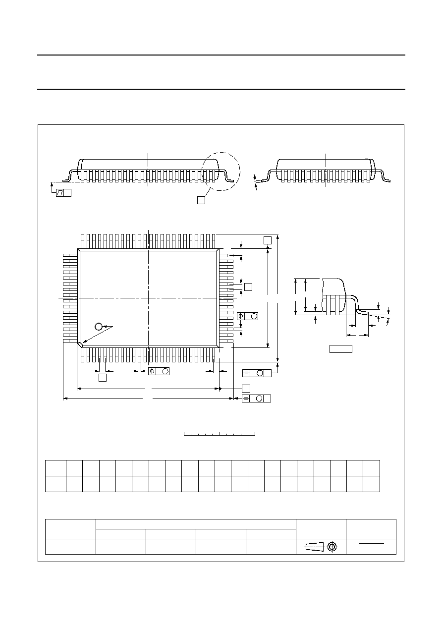
2001 Apr 17
88
Philips Semiconductors
Product specification
Digital telephone answering machine chip
PCD6001
19 PACKAGE OUTLINE
UNIT
A
1
A
2
A
3
b
p
c
E
(1)
e
H
E
L
L
p
Z
y
w
v
REFERENCES
OUTLINE
VERSION
EUROPEAN
PROJECTION
ISSUE DATE
IEC
JEDEC
EIAJ
mm
0.25
0.05
2.90
2.65
0.25
0.45
0.30
0.25
0.14
14.1
13.9
0.8
1.95
18.2
17.6
1.2
0.8
7
0
o
o
0.2
0.2
0.1
DIMENSIONS (mm are the original dimensions)
Note
1. Plastic or metal protrusions of 0.25 mm maximum per side are not included.
1.0
0.6
SOT318-2
MO-112
D
(1)
(1)
(1)
20.1
19.9
H
D
24.2
23.6
E
Z
1.0
0.6
D
b
p
e
E
A
1
A
L
p
detail X
L
(A )
3
B
24
c
b
p
E
H
A
2
D
Z D
A
Z E
e
v
M
A
1
80
65
64
41
40
25
pin 1 index
X
y
D
H
v
M
B
w
M
w
M
97-08-01
99-12-27
0
5
10 mm
scale
QFP80: plastic quad flat package; 80 leads (lead length 1.95 mm); body 14 x 20 x 2.8 mm
SOT318-2
A
max.
3.2

2001 Apr 17
89
Philips Semiconductors
Product specification
Digital telephone answering machine chip
PCD6001
20 SOLDERING
20.1
Introduction to soldering surface mount
packages
This text gives a very brief insight to a complex technology.
A more in-depth account of soldering ICs can be found in
our
"Data Handbook IC26; Integrated Circuit Packages"
(document order number 9398 652 90011).
There is no soldering method that is ideal for all surface
mount IC packages. Wave soldering is not always suitable
for surface mount ICs, or for printed-circuit boards with
high population densities. In these situations reflow
soldering is often used.
20.2
Reflow soldering
Reflow soldering requires solder paste (a suspension of
fine solder particles, flux and binding agent) to be applied
to the printed-circuit board by screen printing, stencilling or
pressure-syringe dispensing before package placement.
Several methods exist for reflowing; for example,
infrared/convection heating in a conveyor type oven.
Throughput times (preheating, soldering and cooling) vary
between 100 and 200 seconds depending on heating
method.
Typical reflow peak temperatures range from
215 to 250
∞
C. The top-surface temperature of the
packages should preferable be kept below 230
∞
C.
20.3
Wave soldering
Conventional single wave soldering is not recommended
for surface mount devices (SMDs) or printed-circuit boards
with a high component density, as solder bridging and
non-wetting can present major problems.
To overcome these problems the double-wave soldering
method was specifically developed.
If wave soldering is used the following conditions must be
observed for optimal results:
∑
Use a double-wave soldering method comprising a
turbulent wave with high upward pressure followed by a
smooth laminar wave.
∑
For packages with leads on two sides and a pitch (e):
≠ larger than or equal to 1.27 mm, the footprint
longitudinal axis is preferred to be parallel to the
transport direction of the printed-circuit board;
≠ smaller than 1.27 mm, the footprint longitudinal axis
must be parallel to the transport direction of the
printed-circuit board.
The footprint must incorporate solder thieves at the
downstream end.
∑
For packages with leads on four sides, the footprint must
be placed at a 45
∞
angle to the transport direction of the
printed-circuit board. The footprint must incorporate
solder thieves downstream and at the side corners.
During placement and before soldering, the package must
be fixed with a droplet of adhesive. The adhesive can be
applied by screen printing, pin transfer or syringe
dispensing. The package can be soldered after the
adhesive is cured.
Typical dwell time is 4 seconds at 250
∞
C.
A mildly-activated flux will eliminate the need for removal
of corrosive residues in most applications.
20.4
Manual soldering
Fix the component by first soldering two
diagonally-opposite end leads. Use a low voltage (24 V or
less) soldering iron applied to the flat part of the lead.
Contact time must be limited to 10 seconds at up to
300
∞
C.
When using a dedicated tool, all other leads can be
soldered in one operation within 2 to 5 seconds between
270 and 320
∞
C.

2001 Apr 17
90
Philips Semiconductors
Product specification
Digital telephone answering machine chip
PCD6001
20.5
Suitability of surface mount IC packages for wave and reflow soldering methods
Notes
1. All surface mount (SMD) packages are moisture sensitive. Depending upon the moisture content, the maximum
temperature (with respect to time) and body size of the package, there is a risk that internal or external package
cracks may occur due to vaporization of the moisture in them (the so called popcorn effect). For details, refer to the
Drypack information in the
"Data Handbook IC26; Integrated Circuit Packages; Section: Packing Methods".
2. These packages are not suitable for wave soldering as a solder joint between the printed-circuit board and heatsink
(at bottom version) can not be achieved, and as solder may stick to the heatsink (on top version).
3. If wave soldering is considered, then the package must be placed at a 45
∞
angle to the solder wave direction.
The package footprint must incorporate solder thieves downstream and at the side corners.
4. Wave soldering is only suitable for LQFP, TQFP and QFP packages with a pitch (e) equal to or larger than 0.8 mm;
it is definitely not suitable for packages with a pitch (e) equal to or smaller than 0.65 mm.
5. Wave soldering is only suitable for SSOP and TSSOP packages with a pitch (e) equal to or larger than 0.65 mm; it is
definitely not suitable for packages with a pitch (e) equal to or smaller than 0.5 mm.
PACKAGE
SOLDERING METHOD
WAVE
REFLOW
(1)
BGA, LFBGA, SQFP, TFBGA
not suitable
suitable
HBCC, HLQFP, HSQFP, HSOP, HTQFP, HTSSOP, SMS
not suitable
(2)
suitable
PLCC
(3)
, SO, SOJ
suitable
suitable
LQFP, QFP, TQFP
not recommended
(3)(4)
suitable
SSOP, TSSOP, VSO
not recommended
(5)
suitable

2001 Apr 17
91
Philips Semiconductors
Product specification
Digital telephone answering machine chip
PCD6001
21 DATA SHEET STATUS
Notes
1. Please consult the most recently issued data sheet before initiating or completing a design.
2. The product status of the device(s) described in this data sheet may have changed since this data sheet was
published. The latest information is available on the Internet at URL http://www.semiconductors.philips.com.
DATA SHEET STATUS
(1)
PRODUCT
STATUS
(2)
DEFINITIONS
Objective data
Development
This data sheet contains data from the objective specification for product
development. Philips Semiconductors reserves the right to change the
specification in any manner without notice.
Preliminary data
Qualification
This data sheet contains data from the preliminary specification.
Supplementary data will be published at a later date. Philips
Semiconductors reserves the right to change the specification without
notice, in order to improve the design and supply the best possible
product.
Product data
Production
This data sheet contains data from the product specification. Philips
Semiconductors reserves the right to make changes at any time in order
to improve the design, manufacturing and supply. Changes will be
communicated according to the Customer Product/Process Change
Notification (CPCN) procedure SNW-SQ-650A.
22 DEFINITIONS
Short-form specification
The data in a short-form
specification is extracted from a full data sheet with the
same type number and title. For detailed information see
the relevant data sheet or data handbook.
Limiting values definition
Limiting values given are in
accordance with the Absolute Maximum Rating System
(IEC 60134). Stress above one or more of the limiting
values may cause permanent damage to the device.
These are stress ratings only and operation of the device
at these or at any other conditions above those given in the
Characteristics sections of the specification is not implied.
Exposure to limiting values for extended periods may
affect device reliability.
Application information
Applications that are
described herein for any of these products are for
illustrative purposes only. Philips Semiconductors make
no representation or warranty that such applications will be
suitable for the specified use without further testing or
modification.
23 DISCLAIMERS
Life support applications
These products are not
designed for use in life support appliances, devices, or
systems where malfunction of these products can
reasonably be expected to result in personal injury. Philips
Semiconductors customers using or selling these products
for use in such applications do so at their own risk and
agree to fully indemnify Philips Semiconductors for any
damages resulting from such application.
Right to make changes
Philips Semiconductors
reserves the right to make changes, without notice, in the
products, including circuits, standard cells, and/or
software, described or contained herein in order to
improve design and/or performance. Philips
Semiconductors assumes no responsibility or liability for
the use of any of these products, conveys no licence or title
under any patent, copyright, or mask work right to these
products, and makes no representations or warranties that
these products are free from patent, copyright, or mask
work right infringement, unless otherwise specified.

2001 Apr 17
92
Philips Semiconductors
Product specification
Digital telephone answering machine chip
PCD6001
24 PURCHASE OF PHILIPS I
2
C COMPONENTS
Purchase of Philips I
2
C components conveys a license under the Philips' I
2
C patent to use the
components in the I
2
C system provided the system conforms to the I
2
C specification defined by
Philips. This specification can be ordered using the code 9398 393 40011.

2001 Apr 17
93
Philips Semiconductors
Product specification
Digital telephone answering machine chip
PCD6001
NOTES

2001 Apr 17
94
Philips Semiconductors
Product specification
Digital telephone answering machine chip
PCD6001
NOTES

2001 Apr 17
95
Philips Semiconductors
Product specification
Digital telephone answering machine chip
PCD6001
NOTES

© Philips Electronics N.V.
SCA
All rights are reserved. Reproduction in whole or in part is prohibited without the prior written consent of the copyright owner.
The information presented in this document does not form part of any quotation or contract, is believed to be accurate and reliable and may be changed
without notice. No liability will be accepted by the publisher for any consequence of its use. Publication thereof does not convey nor imply any license
under patent- or other industrial or intellectual property rights.
Internet: http://www.semiconductors.philips.com
2001
72
Philips Semiconductors ≠ a worldwide company
For all other countries apply to: Philips Semiconductors,
Marketing Communications, Building BE-p, P.O. Box 218, 5600 MD EINDHOVEN,
The Netherlands, Fax. +31 40 27 24825
Argentina: see South America
Australia: 3 Figtree Drive, HOMEBUSH, NSW 2140,
Tel. +61 2 9704 8141, Fax. +61 2 9704 8139
Austria: Computerstr. 6, A-1101 WIEN, P.O. Box 213,
Tel. +43 1 60 101 1248, Fax. +43 1 60 101 1210
Belarus: Hotel Minsk Business Center, Bld. 3, r. 1211, Volodarski Str. 6,
220050 MINSK, Tel. +375 172 20 0733, Fax. +375 172 20 0773
Belgium: see The Netherlands
Brazil: see South America
Bulgaria: Philips Bulgaria Ltd., Energoproject, 15th floor,
51 James Bourchier Blvd., 1407 SOFIA,
Tel. +359 2 68 9211, Fax. +359 2 68 9102
Canada: PHILIPS SEMICONDUCTORS/COMPONENTS,
Tel. +1 800 234 7381, Fax. +1 800 943 0087
China/Hong Kong: 501 Hong Kong Industrial Technology Centre,
72 Tat Chee Avenue, Kowloon Tong, HONG KONG,
Tel. +852 2319 7888, Fax. +852 2319 7700
Colombia: see South America
Czech Republic: see Austria
Denmark: Sydhavnsgade 23, 1780 COPENHAGEN V,
Tel. +45 33 29 3333, Fax. +45 33 29 3905
Finland: Sinikalliontie 3, FIN-02630 ESPOO,
Tel. +358 9 615 800, Fax. +358 9 6158 0920
France: 7 - 9 Rue du Mont ValÈrien, BP317, 92156 SURESNES Cedex,
Tel. +33 1 4728 6600, Fax. +33 1 4728 6638
Germany: Hammerbrookstraþe 69, D-20097 HAMBURG,
Tel. +49 40 2353 60, Fax. +49 40 2353 6300
Hungary: Philips Hungary Ltd., H-1119 Budapest, Fehervari ut 84/A,
Tel: +36 1 382 1700, Fax: +36 1 382 1800
India: Philips INDIA Ltd, Band Box Building, 2nd floor,
254-D, Dr. Annie Besant Road, Worli, MUMBAI 400 025,
Tel. +91 22 493 8541, Fax. +91 22 493 0966
Indonesia: PT Philips Development Corporation, Semiconductors Division,
Gedung Philips, Jl. Buncit Raya Kav.99-100, JAKARTA 12510,
Tel. +62 21 794 0040 ext. 2501, Fax. +62 21 794 0080
Ireland: Newstead, Clonskeagh, DUBLIN 14,
Tel. +353 1 7640 000, Fax. +353 1 7640 200
Israel: RAPAC Electronics, 7 Kehilat Saloniki St, PO Box 18053,
TEL AVIV 61180, Tel. +972 3 645 0444, Fax. +972 3 649 1007
Italy: PHILIPS SEMICONDUCTORS, Via Casati, 23 - 20052 MONZA (MI),
Tel. +39 039 203 6838, Fax +39 039 203 6800
Japan: Philips Bldg 13-37, Kohnan 2-chome, Minato-ku,
TOKYO 108-8507, Tel. +81 3 3740 5130, Fax. +81 3 3740 5057
Korea: Philips House, 260-199 Itaewon-dong, Yongsan-ku, SEOUL,
Tel. +82 2 709 1412, Fax. +82 2 709 1415
Malaysia: No. 76 Jalan Universiti, 46200 PETALING JAYA, SELANGOR,
Tel. +60 3 750 5214, Fax. +60 3 757 4880
Mexico: 5900 Gateway East, Suite 200, EL PASO, TEXAS 79905,
Tel. +9-5 800 234 7381, Fax +9-5 800 943 0087
Middle East: see Italy
Netherlands: Postbus 90050, 5600 PB EINDHOVEN, Bldg. VB,
Tel. +31 40 27 82785, Fax. +31 40 27 88399
New Zealand: 2 Wagener Place, C.P.O. Box 1041, AUCKLAND,
Tel. +64 9 849 4160, Fax. +64 9 849 7811
Norway: Box 1, Manglerud 0612, OSLO,
Tel. +47 22 74 8000, Fax. +47 22 74 8341
Pakistan: see Singapore
Philippines: Philips Semiconductors Philippines Inc.,
106 Valero St. Salcedo Village, P.O. Box 2108 MCC, MAKATI,
Metro MANILA, Tel. +63 2 816 6380, Fax. +63 2 817 3474
Poland: Al.Jerozolimskie 195 B, 02-222 WARSAW,
Tel. +48 22 5710 000, Fax. +48 22 5710 001
Portugal: see Spain
Romania: see Italy
Russia: Philips Russia, Ul. Usatcheva 35A, 119048 MOSCOW,
Tel. +7 095 755 6918, Fax. +7 095 755 6919
Singapore: Lorong 1, Toa Payoh, SINGAPORE 319762,
Tel. +65 350 2538, Fax. +65 251 6500
Slovakia: see Austria
Slovenia: see Italy
South Africa: S.A. PHILIPS Pty Ltd., 195-215 Main Road Martindale,
2092 JOHANNESBURG, P.O. Box 58088 Newville 2114,
Tel. +27 11 471 5401, Fax. +27 11 471 5398
South America: Al. Vicente Pinzon, 173, 6th floor,
04547-130 S√O PAULO, SP, Brazil,
Tel. +55 11 821 2333, Fax. +55 11 821 2382
Spain: Balmes 22, 08007 BARCELONA,
Tel. +34 93 301 6312, Fax. +34 93 301 4107
Sweden: Kottbygatan 7, Akalla, S-16485 STOCKHOLM,
Tel. +46 8 5985 2000, Fax. +46 8 5985 2745
Switzerland: Allmendstrasse 140, CH-8027 ZÐRICH,
Tel. +41 1 488 2741 Fax. +41 1 488 3263
Taiwan: Philips Semiconductors, 5F, No. 96, Chien Kuo N. Rd., Sec. 1,
TAIPEI, Taiwan Tel. +886 2 2134 2451, Fax. +886 2 2134 2874
Thailand: PHILIPS ELECTRONICS (THAILAND) Ltd.,
60/14 MOO 11, Bangna Trad Road KM. 3, Bagna, BANGKOK 10260,
Tel. +66 2 361 7910, Fax. +66 2 398 3447
Turkey: Yukari Dudullu, Org. San. Blg., 2.Cad. Nr. 28 81260 Umraniye,
ISTANBUL, Tel. +90 216 522 1500, Fax. +90 216 522 1813
Ukraine: PHILIPS UKRAINE, 4 Patrice Lumumba str., Building B, Floor 7,
252042 KIEV, Tel. +380 44 264 2776, Fax. +380 44 268 0461
United Kingdom: Philips Semiconductors Ltd., 276 Bath Road, Hayes,
MIDDLESEX UB3 5BX, Tel. +44 208 730 5000, Fax. +44 208 754 8421
United States: 811 East Arques Avenue, SUNNYVALE, CA 94088-3409,
Tel. +1 800 234 7381, Fax. +1 800 943 0087
Uruguay: see South America
Vietnam: see Singapore
Yugoslavia: PHILIPS, Trg N. Pasica 5/v, 11000 BEOGRAD,
Tel. +381 11 3341 299, Fax.+381 11 3342 553
Printed in The Netherlands
403506/02/pp
96
Date of release:
2001 Apr 17
Document order number:
9397 750 08241