
Philips
Semiconductors
PDI1394P21
3-port physical layer interface
Objective specification
1999 Jul 09
INTEGRATED CIRCUITS

Philips Semiconductors
Objective specification
PDI1394P21
3-port physical layer interface
2
1999 Jul 09
1.0
FEATURES
∑
Fully supports provisions of IEEE 1394≠1995 Standard for high
performance serial bus and the P1394a supplement (Version 2.0)
1
∑
Full P1394a support includes:
≠ Connection debounce
≠ Arbitrated short reset
≠ Multispeed concatenation
≠ Arbitration acceleration
≠ Fly-by concatenation
≠ Port disable/suspend/resume
∑
Provides three 1394a fully-compliant cable ports at
100/200/400 Megabits per second (Mbits/s)
∑
Fully compliant with Open HCI requirements
∑
Cable ports monitor line conditions for active connection to remote
node.
∑
Power down features to conserve energy in battery-powered
applications include:
≠ Automatic device power down during suspend
≠ Device power down terminal
≠ Link interface disable via LPS
≠ Inactive ports powered-down
∑
Logic performs system initialization and arbitration functions
∑
Encode and decode functions included for data-strobe bit level
encoding
∑
Incoming data resynchronized to local clock
∑
Single 3.3 volt supply operation
∑
Minimum V
DD
of 2.7 V for end-of-wire power-consuming devices
∑
While unpowered and connected to the bus, will not drive TPBIAS
on a connected port, even if receiving incoming bias voltage on
that port
∑
Supports extended bias-handshake time for enhanced
interoperability with camcorders
∑
Interface to link-layer controller supports low-cost bus-holder
isolation and optional Annex J electrical isolation
∑
Data interface to link-layer controller through 2/4/8 parallel lines at
49.152 MHz
∑
Low-cost 24.576 MHz crystal provides transmit, receive data at
100/200/400 Mbits/s, and link-layer controller clock at 49.152 MHz
∑
Does not require external filter capacitors for PLL
∑
Interoperable with link-layer controllers using 3.3 V and 5 V
supplies
∑
Interoperable with other Physical Layers (PHYs) using 3.3 V and
5 V supplies
∑
Node power class information signaling for system power
management
∑
Cable power presence monitoring
∑
Separate cable bias (TPBIAS) for each port
∑
Register bits give software control of contender bit, power class
bits, link active bit, and 1394a features
∑
Fully interoperable with FireWire
TM
implementation of IEEE Std 1394
∑
Function and pin compatible with the Texas Instruments 400 Mbps
Phy TSB41LV03
TM
2.0
DESCRIPTION
The PDI1394P21 provides the digital and analog transceiver functions
needed to implement a three port node in a cable-based IEEE
1394≠1995 and/or 1394a network. Each cable port incorporates two
differential line transceivers. The transceivers include circuitry to
monitor the line conditions as needed for determining connection
status, for initialization and arbitration, and for packet reception and
transmission. The PDI1394P21 is designed to interface with a Link
Layer Controller (LLC), such as the PDI1394L11 or PDI1394L21.
3.0
ORDERING INFORMATION
PACKAGE
TEMPERATURE RANGE
OUTSIDE NORTH AMERICA
NORTH AMERICA
PKG. DWG. #
80-pin plastic LQFP
0
∞
C to +70
∞
C
PDI1394P21 BE
PDI1394P21 BE
SOT315-1
1.
Implements technology covered by one or more patents of Apple Computer, Incorporated and SGS Thompson, Limited.
Philips Semiconductors
Objective specification
PDI1394P21
3-port physical layer interface
1999 Jul 09
3
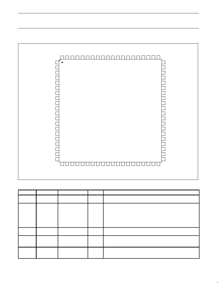
4.0
PIN CONFIGURATION
NC
1
2
3
4
5
6
7
23
24
25
26
27
28
29
LREQ
SYSCLK
DGND
CTL0
CTL1
D0
DVDD
30
31
21
22
8
9
10
11
D1
NC
D3
D2
PDI1394P21
12
13
14
15
16
17
D4
D5
D6
D7
CNA
DGND
18
19
20
PD
LPS
DGND
32
33
34
35
36
DGND
C/LKON
PC0
PC1
PC2
/ISO
CPS
DGND
DVDD
DVDD
NC
TEST1
TEST0
A
VDD
A
VDD
AGND
60
59
58
57
56
55
54
AGND
TPBIAS2
TPA2+
TPA2≠
TPB2+
AVDD
TPB2≠
53
52
51
50
TPBIAS1
TPA1+
TPB1+
TPA1≠
49
48
47
46
45
44
TPB1≠
AVDD
AVDD
TPBIAS0
TPA0≠
TPA0+
43
42
41
TPB0+
TPB0≠
AGND
78
77
76
75
74
73
72
71
70
80
79
69
68
67
66
65
DGND
DVDD
/RESET
XO
XI
PLLGND
PLLGND
PLL
VDD
NC
DGND
DVDD
DVDD
R1
R0
AGND
37
38
39
40
64
63
62
61
AGND
AGND
AGND
AGND
AGND
A
VDD
A
VDD
AGND
SV001742
5.0
PIN DESCRIPTION
Name
Pin Type
Pin Numbers
I/O
Description
AGND
Supply
36, 37, 38, 39, 40,
41, 60, 61, 64, 65
--
Analog circuit ground terminals. These terminals should be tied together
to the low impedance circuit board ground plane.
AVDD
Supply
34, 35, 47, 48, 54,
62, 63
--
Analog circuit power terminals. A combination of high frequency
decoupling capacitors near each terminal are suggested, such as
paralleled 0.1
µ
F and 0.001
µ
F. Lower frequency 10
µ
F filtering
capacitors are also recommended. These supply terminals are
separated from PLLVDD and DVDD internal to the device to provide
noise isolation. They should be tied at a low impedance point on the
circuit board.
CNA
CMOS
17
O
Cable Not Active output. This terminal is asserted high when there are
no ports receiving incoming bias voltage.
CPS
CMOS
27
I
Cable Power Status input. This terminal is normally connected to cable
power through a 370≠410 k
resistor. This circuit drives an internal
comparator that is used to detect the presence of cable power.
CTL0,
CTL1
CMOS 5V tol
4, 5
I/O
Control I/Os. These bi-directional signals control communication
between the PDI1394P21 and the LLC. Bus holders are built into
these terminals.

Philips Semiconductors
Objective specification
PDI1394P21
3-port physical layer interface
1999 Jul 09
4
Name
Description
I/O
Pin Numbers
Pin Type
C/LKON
CMOS 5V tol
22
I/O
Bus Manager Contender programming input and link-on output. On
hardware reset, this terminal is used to set the default value of the
contender status indicated during self-ID. Programming is done by tying
the terminal through a 10k
resistor to a high (contender) or low (not
contender). The resistor allows the link-on output to override the input.
Following hardware reset, this terminal is the link-on output, which is
used to notify the LLC to power-up and become active. The link-on
output is a square-wave signal with a period of approximately 163 ns (8
SYSCLK cycles) when active. The link-on output is deasserted low when
the LPS input terminal is active.
DGND
Supply
3, 16, 20, 21, 28,
70, 80
--
Digital circuit ground terminals. These terminals should be tied together
to the low impedance circuit board ground plane.
D0≠D7
CMOS 5V tol
7, 8, 10, 11, 12, 13,
14, 15
I/O
Data I/Os. These are bi-directional data signals between the
PDI1394P21 and the LLC. Bus holders are built into these terminals.
DVDD
Supply
6, 29, 30, 68, 69, 79
--
Digital circuit power terminals. A combination of high frequency
decoupling capacitors near each terminal are suggested, such as
paralleled 0.1
µ
F and 0.001
µ
F. Lower frequency 10
µ
F filtering
capacitors are also recommended. These supply terminals are
separated from PLLVDD and AVDD internal to the device to provide
noise isolation. They should be tied at a low impedance point on the
circuit board.
/ISO
CMOS
26
I
Link interface isolation control input. This terminal controls the operation
of output differentiation logic on the CTL and D terminals. If an optional
isolation barrier of the type described in Annex J of IEEE Std 1394≠1395
is implemented between the PDI1394P21 and LLC, the /ISO terminal
should be tied low to enable the differentiation logic. If no isolation barrier
is implemented (direct connection), or bus holder isolation is
implemented, the /ISO terminal should be tied high to disable the
differentiation logic.
LPS
CMOS 5V tol
19
I
Link Power Status input. This terminal is used to monitor the power
status of the LLC, and is connected to either the V
DD
supplying the link
layer controller through a 1k
resistor, or to a pulsed output which is
active when the LLC is powered. The pulsed output is useful when using
an isolation barrier. If this input is low for more than 25
m
s, the LLC is
considered powered down. If this input is high for more than 20 ns, the
LLC is considered powered up. If the LLC is powered-down, the
PHY≠LLC interface is disabled, and the PDI1394P21 performs only the
basic repeater functions required for network initialization and operation.
Bus holder is built into this terminal.
LREQ
CMOS 5V tol
1
I
LLC Request input. The LLC uses this input to initiate a service request
to the PDI1394P21. Bus holder is built into this terminal.
NC
No Connect
9, 31, 71, 72
--
These pins are not internally connected, and consequently are "don't
cares". Other vendor's pin compatible chips may require connections
and external circuitry on these pins.
PC0, PC1,
PC2
CMOS 5V tol
23, 24, 25
I
Power Class programming inputs. On hardware reset, these inputs set
the default value of the power class indicated during self-ID.
Programming is done by tying the terminals high or low. Refer to
Table 18 for encoding.
PD
CMOS 5V tol
18
I
Power Down input. A logic high on this terminal turns off all internal
circuitry except the cable-active monitor circuits which control the CNA
output. Bus holder is built into this terminal. For more information, refer to
Section 17.3
PLLGND
Supply
74, 75
--
PLL circuit ground terminals. These terminals should be tied together to
the low impedance circuit board ground plane.
PLLVDD
Supply
73
--
PLL circuit power terminals. A combination of high frequency decoupling
capacitors near each terminal are suggested, such as paralleled 0.1
µ
F
and 0.001
µ
F. Lower frequency 10
µ
F filtering capacitors are also
recommended. These supply terminals are separated from DVDD and
AVDD internal to the device to provide noise isolation. They should be
tied at a low impedance point on the circuit board.

Philips Semiconductors
Objective specification
PDI1394P21
3-port physical layer interface
1999 Jul 09
5
Name
Description
I/O
Pin Numbers
Pin Type
/RESET
CMOS 5V tol
78
I
Logic reset input. Asserting this terminal low resets the internal logic. An
internal pull-up resistor to V
DD
is provided so only an external
delay capacitor in parallel with a resistor is required for proper power-up
operation. For more information, refer to Section 17.3. This input is
otherwise a standard logic input, and can also be driven by an
open-drain type driver.
R0, R1
Bias
66, 67
--
Current setting resistor terminals. These terminals are connected to
an external resistance to set the internal operating currents and
cable driver output currents. A resistance of 6.34 k
±
1% is required to
meet the IEEE Std 1394≠1995 output voltage limits.
SYSCLK
CMOS
2
O
System clock output. Provides a 49.152 MHz clock signal, synchronized
with data transfers, to the LLC.
TEST0
CMOS
33
I
Test control input. This input is used in manufacturing tests of the
PDI1394P21. For normal use, this terminal should be tied to GND.
TEST1
CMOS
32
I
Test control input. This input is used in manufacturing tests of the
PDI1394P21. For normal use, this terminal should be tied to GND.
TPA0+,
TPA1+,
TPA2+
Cable
45, 52, 58
I/O
Twisted-pair cable A differential signal terminals. Board traces from each
pair of positive and negative differential signal terminals should be kept
TPA0≠,
TPA1≠,
TPA2≠
Cable
44, 51, 57
I/O
g
g
matched and as short as possible to the external load resistors and to
the cable connector.
TPB0+,
TPB1+,
TPB2+
Cable
43, 50, 56
I/O
Twisted-pair cable B differential signal terminals. Board traces from each
pair of positive and negative differential signal terminals should be kept
TPB0≠,
TPB1≠,
TPB2≠
Cable
42, 49, 55
I/O
g
g
matched and as short as possible to the external load resistors and to
the cable connector.
TPBIAS0,
TPBIAS1,
TPBIAS2
Cable
46, 53, 59
I/O
Twisted-pair bias output. This provides the 1.86V nominal bias voltage
needed for proper operation of the twisted-pair cable drivers and
receivers, and for signaling to the remote nodes that there is an active
cable connection. Each of these terminals must be decoupled with a
0.3
µ
F≠1
µ
F capacitor to ground.
XO, XI
Crystal
77, 76
--
Crystal oscillator inputs. These terminals connect to a 24.576 MHz
parallel resonant fundamental mode crystal. The optimum values for the
external shunt capacitors are dependent on the specifications of the
crystal used. Can also be driven by an external clock generator (leave
XO unconnected in this case).

Philips Semiconductors
Objective specification
PDI1394P21
3-port physical layer interface
1999 Jul 09
6
6.0
BLOCK DIAGRAM
CABLE PORT 0
CABLE PORT 1
CABLE PORT 2
RECEIVED DATA
DECODER/
RETIMER
LINK
INTERFACE
I/O
ARBITRATION
AND CONTROL
STATE MACHINE
LOGIC
CRYSTAL
OSCILLATOR,
PLL SYSTEM,
AND CLOCK
GENERATOR
TRANSMIT
DATA
ENCODER
CNA
PC0
PC1
PC2
D0
D1
D2
D3
CTL0
CTL1
LREQ
SYSCLK
C/LKON
/ISO
LPS
CPS
/RESET
PD
TPA0+
TPA0≠
TPB0+
TPB0≠
TPA1+
TPA1≠
TPB1+
TPB1≠
TPA2+
TPA2≠
TPB2+
TPB2≠
XI
XO
SV01743
D4
D5
D6
D7
BIAS VOLTAGE
AND
CURRENT
GENERATOR
R0
R1
TPBIAS0
TPBIAS1
TPBIAS2
CABLE POWER
DETECTOR
CPS
7.0
FUNCTIONAL SPECIFICATION
The PDI1394P21 requires only an external 24.576 MHz crystal as a
reference. An external clock can be provided instead of a crystal. An
internal oscillator drives an internal phase-locked loop (PLL), which
generates the required 393.216 MHz reference signal. This
reference signal is internally divided to provide the clock signals
used to control transmission of the outbound encoded Strobe and
Data information. A 49.152 MHz clock signal, supplied to the
associated LLC for synchronization of the two chips, is used for
resynchronization of the received data. The Power Down (PD)
function, when enabled by asserting the PD terminal high, stops
operation of the PLL and disables all circuits except the cable bias
detectors at the TPB terminals. The port transmitter circuitry and the
receiver circuitry are also disabled when the port is disabled,
suspended, or disconnected.
The PDI1394P21 supports an optional isolation barrier between
itself and its LLC. When the /ISO input terminal is tied high, the
LLC interface outputs behave normally. When the /ISO terminal is
tied low, internal differentiating logic is enabled, and the outputs are
driven such that they can be coupled through a capacitive or
transformer galvanic isolation barrier as described in
IEEE 1394a
section 5.9.4. To operate with single capacitor (bus holder) isolation,
the /ISO on the PHY terminal must be tied high.
Data bits to be transmitted through the cable ports are received from
the LLC on two, four or eight parallel paths (depending on the
requested transmission speed). They are latched internally in the
PDI1394P21 in synchronization with the 49.152 MHz system clock.
These bits are combined serially, encoded, and transmitted at
98.304/196.608/392.216 Mbits/s (referred to as S100, S200, and
S400 speed, respectively) as the outbound data-strobe information
stream. During transmission, the encoded data information is
transmitted differentially on the TPB cable pair(s), and the encoded
strobe information is transmitted differentially on the TPA cable
pair(s).
During packet reception the TPA and TPB transmitters of the
receiving cable port are disabled, and the receivers for that port are
enabled. The encoded data information is received on the TPA cable
pair, and the encoded strobe information is received on the TPB
cable pair. The received data-strobe information is decoded to
recover the receive clock signal and the serial data bits. The serial

Philips Semiconductors
Objective specification
PDI1394P21
3-port physical layer interface
1999 Jul 09
7
data bits are split into two-, four- or eight-bit parallel streams
(depending upon the indicated receive speed), resynchronized to
the local 49.152 MHz system clock and sent to the associated LLC.
The received data is also transmitted (repeated) on the other active
(connected) cable ports.
Both the TPA and TPB cable interfaces incorporate differential
comparators to monitor the line states during initialization and
arbitration. The outputs of these comparators are used by the
internal logic to determine the arbitration status. The TPA channel
monitors the incoming cable common-mode voltage. The value of
this common-mode voltage is used during arbitration to set the
speed of the next packet transmission (speed signalling). In addition,
the TPB channel monitors the incoming cable common-mode
voltage on the TPB pair for the presence of the remotely supplied
twisted-pair bias voltage (cable bias detection).
The PDI1394P21 provides a 1.86 V nominal bias voltage at the
TPBIAS terminal for port termination. the PHY contains three
independent TPBIAS circuits. This bias voltage, when seen through
a cable by a remote receiver, indicates the presence of an active
connection. This bias voltage source must be stabilized by an
external filter capacitor of 0.3
µ
F≠1
µ
F.
The line drivers in the PDI1394P21 operate in a high-impedance
current mode, and are designed to work with external 112
line-termination resistor networks in order to match the 110
cable
impedance. One network is provided at each end of all twisted-pair
cable. Each network is composed of a pair of series-connected 56
resistors. The midpoint of the pair of resistors that is directly
connected to the twisted-pair A terminals is connected to its
corresponding TPBIAS voltage terminal. The midpoint of the pair of
resistors that is directly connected to the twisted-pair B terminals is
coupled to ground through a parallel R-C network with recommended
values of 5 k
and 220 pF. The values of the external line termination
resistors are designed to meet the standard specifications when
connected in parallel with the internal receiver circuits. An external
resistor connected between the R0 and R1 terminals sets the driver
output current, along with other internal operating currents. This
current setting resistor has a value of 6.34 k
±
1%.
When the power supply of the PDI1394P21 is removed while the
twisted-pair cables are connected, the PDI1394P21 transmitter and
receiver circuitry presents a high impedance to the cable in order to
not load the TPBIAS voltage on the other end of the cable.
When the PDI1394P21 is used with one or more of the ports not
brought out to a connector, the twisted-pair terminals of the unused
ports must be terminated for reliable operation. For each unused
port, the TPB+ and TPB≠ terminals can be tied together and then
pulled to ground, or the TPB+ and TPB≠ terminals can be connected
to the suggested termination network. The TPA+ and TPA≠ and
TPBIAS terminals of an unused port can be left unconnected.
The TEST0 and TEST1 terminals are used to set up various
manufacturing test conditions. For normal operation, the TEST0 and
TEST1 terminals should be connected to ground.
Four package terminals, used as inputs to set the default value for
four configuration status bits in the self-ID packet, should be
hard-wired high or low as a function of the equipment design. The
PC0≠PC2 terminals are used to indicate the default power-class
status for the node (the need for power from the cable or the ability
to supply power to the cable). See Table 18 for power class
encoding. The C/LKON terminal is used as an input to indicate that
the node is a contender for bus manager.
The PHY supports suspend/resume as defined in the IEEE 1394a
specification. The suspend mechanism allows pairs of directly
connected ports to be placed into a low power state while
maintaining a port-to-port connection between 1394 bus segments.
While in a low power state, a port is unable to transmit or receive
data transaction packets. However, a port in a low power state is
capable of detecting connection status changes and detecting
incoming TPBIAS. When all three ports of the PDI1394P21 are
suspended, all circuits except the bias-detection circuits are
powered down, resulting in significant power savings. The TPBIAS
circuit monitors the value of incoming TPA pair common-mode
voltage when local TPBIAS is inactive. Because this circuit has an
internal current source and the connected node has a current sink,
the monitored value indicates the cable connection status. This
monitor is called connect-detect.
Both the cable bias-detect monitor and TPBIAS connect-detect
monitor are used in suspend/resume signaling and cable connection
detection. For additional details of suspend/resume operation, refer
to the 1394a specification. The use of suspend/resume is
recommended for new designs.
The port transmitter and receiver circuitry is disabled during power
down (when the PD input terminal is asserted high), during reset
(when the /RESET input terminal is asserted low), when no active
cable is connected to the port, or when controlled by the internal
arbitration logic. The port twisted-pair bias voltage circuitry is
disabled during power down, during reset, or when the port is
disabled as commanded by the LLC.
The CNA (cable-not-active) terminal provides a high output when all
twisted-pair cable ports are disconnected, and can be used along
with LPS to determine when to power down the PDI1394P21. The
CNA output is not debounced. In Power Down mode, the CNA
detection circuitry remains enabled.
The LPS (link power status) terminal works with the C/LKON
terminal to manage the power usage in the node. The LPS signal
from the LLC indicates to the PHY that the LLC is powered up and
active. During LLC Power Down mode, as indicated by the LPS
input being low for more than 25
µ
s, the PDI1394P21 deactivates
the PHY-LLC interface to save power. The PDI1394P21 continues
the necessary repeater function required for network operation
during this low power state.
If the PHY receives a link-on packet from another node, the C/LKON
terminal is activated to output a square-wave signal. The LLC
recognizes this signal, reactivates any powered-down portions of the
LLC, and notifies the PHY of its power-on status via the LPS
terminal. The PHY confirms notification by deactivating the
square-wave signal on the C/LKON terminal, then enables the
PHY-link interface.

Philips Semiconductors
Objective specification
PDI1394P21
3-port physical layer interface
1999 Jul 09
8
8.0
ABSOLUTE MAXIMUM RATINGS
1
In accordance with the Absolute Maximum Rating System (IEC 134). Voltages are referenced to GND (ground = 0 V).
SYMBOL
PARAMETER
CONDITION
LIMITS
UNIT
SYMBOL
PARAMETER
CONDITION
MIN
MAX
UNIT
V
DD
DC supply voltage
≠0.5
4.0
V
V
I
DC input voltage
≠0.5
V
DD
+0.5
V
V
I
≠5V
5 volt tolerant input voltage range
≠0.5
5.5
V
V
O
DC output voltage range at any output
≠0.5
V
DD
+0.5
V
Electrostatic discharge
Human Body Model
2
kV
Electrostatic discharge
Machine Model
200
V
T
amb
Operating free-air temperature range
0
+70
∞
C
T
stg
Storage temperature range
≠65
+150
∞
C
NOTE:
1. Stresses beyond those listed under "Absolute Maximum Ratings" may cause permanent damage to the device. These are stress ratings
only, and functional operation of the device at these or any other conditions beyond those indicated under "Recommended Operating
Conditions" is not implied. Exposure to absolute-maximum-rated conditions for extended periods may affect device reliability.
9.0
RECOMMENDED OPERATING CONDITIONS
SYMBOL
PARAMETER
MIN
TYP
MAX
UNIT
SYMBOL
PARAMETER
MIN
TYP
MAX
UNIT
V
Supply voltage
Source power node
3.0
3.3
3.6
V
V
DD
Supply voltage
Non-source power node
2.7
1
3.0
3.6
V
V
High-level input voltage, pins
/ISO = V
DD
, V
DD
= 2.7 V
2.3
5.5
V
V
IH
g
g ,
CTLn, Dn, C/LKON
2
/ISO = V
DD
, V
DD
>= 3.0 V
2.6
5.5
V
V
IL
Low-level input voltage, pins
CTLn, Dn, C/LKON
2
/ISO = V
DD
0.7
V
I
OH
/I
OL
Output current, pins CTLn, Dn,
C/LKON and SYSCLK
V
OH
= V
DD
≠0.5 V, V
OL
= 0.5 V
≠12
12
mA
I
O
Output current
TPBIAS outputs
≠6
2.5
mA
V
Differential input voltage amplitude
TPA, TPB cable inputs, during data reception
118
260
mV
V
ID
Differential input voltage amplitude
TPA, TPB cable inputs, during data arbitration
168
265
mV
V
C
TPB common mode input voltage
Speed signalling off
Source power node
1.165
2.515
V
V
IC-100
TPB common-mode input voltage
g
g
or S100 speed signal
Non-source power node
1.165
2.015
1
V
V
C
TPB common mode input voltage
S200 speed signal
Source power node
0.935
2.515
V
V
IC-200
TPB common-mode input voltage
S200 speed signal
Non-source power node
0.935
2.015
1
V
V
C
TPB common mode input voltage
S400 speed signal
Source power node
0.523
2.515
V
V
IC-100
TPB common-mode input voltage
S400 speed signal
Non-source power node
0.523
2.015
1
V
t
PU
Power≠up reset time
Set by capacitor between /RESET pin and GND
2
ms
TPA, TPB cable inputs, S100 operation
1.08
ns
Receive input jitter
TPA, TPB cable inputs, S200 operation
0.5
ns
TPA, TPB cable inputs, S400 operation
0.315
ns
Between TPA and TPB cable inputs, S00 operation
0.8
ns
Receive input skew
Between TPA and TPB cable inputs, S200 operation
0.55
ns
Between TPA and TPB cable inputs, S400 operation
0.5
ns
f
XTAL
Crystal or external clock frequency
Crystal connected according to Figure 8 or external
clock input at pin XI
24.5735
24.576
24.5785
MHz
NOTES:
1. For a node that does not source power to the bus (see Section 4.2.2.2 in the IEEE 1394-1995 standard).
2. C/LKON is only an input when /RESET = 0.

Philips Semiconductors
Objective specification
PDI1394P21
3-port physical layer interface
1999 Jul 09
9
10.0
CABLE DRIVER
SYMBOL
PARAMETER
TEST CONDITION
LIMITS
UNIT
SYMBOL
PARAMETER
TEST CONDITION
MIN
TYP
MAX
UNIT
V
OD
Differential output voltage
56
load
172
265
mV
I
O(diff)
Driver Difference current, TPA+, TPA≠, TPB+, TPB≠
1
Drivers enabled,
speed signaling OFF
≠1.05
1
0.88
1
mA
2
100 Mbit/s speed signaling enabled
≠0.81
≠0.44
mA
I
SP
Common mode speed signaling current, TPB+, TPB≠
2
200 Mbit/s speed signaling enabled
≠4.84
≠2.53
mA
400 Mbit/s speed signaling enabled
≠12.4
≠8.10
mA
V
OFF
OFF state differential voltage
Drivers disabled
20
mV
NOTES:
1. Limits defined as algebraic sum of TPA+ and TPA≠ driver currents. Limits also apply to TPB+ and TPB≠ algebraic sum of driver currents.
2. Limits defined as absolute limit of each of TPB+ and TPB≠ driver currents.
11.0
CABLE RECEIVER
SYMBOL
PARAMETER
TEST CONDITION
LIMITS
UNIT
SYMBOL
PARAMETER
TEST CONDITION
MIN
TYP
MAX
UNIT
Z
Differential input impedance
Drivers disabled
10
14
k
Z
ID
Differential input impedance
Drivers disabled
4
pF
Z
C
Common mode input impedance
Drivers disabled
20
k
Z
IC
Common mode input impedance
Drivers disabled
24
pF
V
TH-R
Receiver input threshold voltage
Drivers disabled
≠30
30
mV
V
TH-CB
Cable bias detect threshold, TPBn cable inputs
Drivers disabled
0.6
1.0
V
V
TH+
Positive arbitration comparator threshold voltage
Drivers disabled
89
168
mV
V
TH≠
Negative arbitration comparator threshold voltage
Drivers disabled
≠168
≠89
mV
V
TH≠SP200
Speed signal threshold
TPBIAS≠TPA common mode
voltage, drivers disabled
49
131
mV
V
TH≠SP400
Speed signal threshold
TPBIAS≠TPA common mode
voltage, drivers disabled
314
396
mV
I
CD
Connect detect output at TPBIAS pins
Drivers disabled
76
µ
A

Philips Semiconductors
Objective specification
PDI1394P21
3-port physical layer interface
1999 Jul 09
10
12.0
OTHER DEVICE I/O
SYMBOL
PARAMETER
TEST CONDITION
MIN
TYP
MAX
UNIT
Peak
1
tbf
mA
I
Supply current
Transmit
2
tbf
mA
I
DD
Supply current
Repeat
3
tbf
mA
Idle
4
tbf
mA
I
DD≠PD
Supply current in power down or
suspend mode
PD = V
DD
in power down mode
tbf
tbf
mA
V
TH
Cable power status threshold voltage
370 k
≠400 k
resistor between cable
power and CPS pin: Measured at cable
power side of resistor
7.5
8.0
8.5
V
Hi h l
l
t
t
lt
i
CTL
V
DD
>= 2.7 V, I
OH
= ≠4 mA, /ISO = V
DD
2.2
V
V
OH
High-level output voltage. pins CTLn,
Dn, SYSCLK, CNA, C/LKON
V
DD
>= 3.0 V, I
OH
= ≠4 mA, /ISO = V
DD
2.8
V
Dn, SYSCLK, CNA, C/LKON
Annex J: I
OH
= ≠9 mA, /ISO = 0
V
DD
≠0.4
V
V
O
Low level output voltage
I
OL
= 4 mA, /ISO = V
DD
0.4
V
V
OL
Low-level output voltage
Annex J: I
OL
= 9 mA, /ISO = 0
0.4
V
I
BH+
Positive peak bus holder current
/ISO = V
DD
, V
I
= 0 V to V
DD
0.08
0.25
mA
I
BH≠
Negative peak bus holder current
/ISO = V
DD
, V
I
= 0 V to V
DD
≠0.25
≠0.08
mA
I
I
Input current, pins LREQ, LPS, PD,
TEST0, TEST1, PC0≠PC2
/ISO = 0 V; V
DD
= 3.6 V
5
µ
A
I
OZ
Off-state current, pins CTLn, Dn,
C/LKON
VO = V
DD
or 0 V
≠5
5
µ
A
I
S
Pullup current /RESET input
V
I
= 1.5 V, PD = 0
≠80
≠40
≠20
µ
A
I
RST-UP
Pullup current, /RESET input
V
I
= 0 V, PD = 0
≠90
≠45
≠22
µ
A
I
RST-DN
Pulldown current, /RESET input
V
I
= V
DD
, PD = V
DD
86
260
450
µ
A
V
IT+
Positive going threshold voltage, LREQ,
CTL0, CTL1, D0≠D7, C/LKON inputs
5
/ISO = 0 V
V
DD
/2 + 0.3
V
DD
/2 + 0.9
V
V
IT≠
Negative going threshold voltage, LREQ,
CTL0, CTL1, D0≠D7, C/LKON inputs
5
/ISO = 0 V
V
DD
/2 ≠ 0.9
V
DD
/2 ≠ 0.3
V
V
IT+
Positive going threshold voltage, PD,
LPS inputs
/ISO = 0 V. V
LREF
= 0.42 x V
DD
V
LREF
+1
V
V
IT≠
Negative going threshold voltage, PD,
LPS inputs
/ISO = 0 V. V
LREF
= 0.42 x V
DD
V
LREF
+0.2
V
V
O
TPBIAS output voltage
At rated I
O
current
1.665
2.015
V
NOTES:
1. Worst case, all ports transmitting, 100% bandwidth at S400, V
DD
= 3.6 V, T
A
= 0
∞
C: At T
A
= 70
∞
C, the maximum current is tbf mA.
2. All ports transmitting, 100% bandwidth at S400, V
DD
= 3.3 V, T
A
= 25
∞
C
3. Receiving on port 0 and transmitting on port 1 and port 2. Full ISO payload of 84
µ
S, S400, data value of CCCCCCCCh, V
DD
= 3.3 V, TA = 25
∞
C
4. Receiving cycle starts on port 0 and transmitting cycle starts on port 1 and port 2, V
DD
= 3.3 V, TA = 25
∞
C
5. C/LKON is only an input when /RESET = 0

Philips Semiconductors
Objective specification
PDI1394P21
3-port physical layer interface
1999 Jul 09
11
13.0
THERMAL CHARACTERISTICS
SYMBOL
PARAMETER
TEST CONDITION
LIMITS
UNIT
SYMBOL
PARAMETER
TEST CONDITION
MIN
TYP
MAX
UNIT
R
jA
Junction-to-free-air thermal resistance
Board mounted, no air flow
TBD
∞
C/W
14.0
AC CHARACTERISTICS
SYMBOL
PARAMETER
CONDITION
MIN
TYP
MAX
UNIT
Transmit jitter
TPA, TPB
0.15
ns
Transmit skew
Between TPA and TPB
0.10
ns
t
r
TPA, TPB differential output voltage rise time
10% to 90%; At 1394 connector
0.5
1.2
ns
t
f
TPA, TPB differential output voltage fall time
90% to 10%; At 1394 connector
0.5
1.2
ns
t
SU
Setup time, CTL0, CTL1, D1≠D7, LREQ to SYSCLK
50% to 50%; See Figure 2
5
ns
t
H
Hold time, CTL0, CTL1, D1≠D7, LREQ after SYSCLK
50% to 50%; See Figure 2
0
ns
t
D
Delay time SYSCLK to CTL0, CTL1, D1≠D7
50% to 50%; See Figure 3
0.5
11
ns
15.0
TIMING WAVEFORMS
SV01098
56
TPAn+
TPBn+
TPAn≠
TPBn≠
Figure 1.
Test load diagram
SV01099
t
SU
t
H
SYSCLK
Dn, CTLn, LREQ
Figure 2.
Dn, CTLn, LREQ input setup and hold times
SV01100
t
D
SYSCLK
Dn, CTLn, LREQ
Figure 3.
Dn, CTLn, output delay relative to SYSCLK

Philips Semiconductors
Objective specification
PDI1394P21
3-port physical layer interface
1999 Jul 09
12
16.0
INTERNAL REGISTER CONFIGURATION
There are 16 accessible internal registers in the PDI1394P21. The
configuration of the registers at addresses 0 through 7 (the base
registers) is fixed, while the configuration of the registers at
addresses 8h through Fh (the paged registers) is dependent upon
which one of eight pages, numbered 0h through 7h, is currently
selected. The selected page is set in base register 7h.
The configuration of the base registers is shown in Table 1, and
corresponding field descriptions are given in Table 2. The base
register field definitions are unaffected by the selected page number.
A reserved register or register field (marked as Reserved or Rsvd in
the following register configuration tables) is read as 0, but is subject
to future usage. All registers in address pages 2 through 6 are
reserved.
Table 1. Base Register Configuration
ADDRESS
BIT POSITION
ADDRESS
0
1
2
3
4
5
6
7
0000
Physical ID
R
CPS
0001
RHB
IBR
Gap_Count
0010
Extended (111b)
Rsvd
Num_Ports (0011b)
0011
PHY_Speed (010b)
Rsvd
Delay (0000b)
0100
L
C
Jitter (000)
Pwr_Class
0101
RPIE
ISBR
CTOI
CPSI
STOI
PEI
EAA
EMC
0110
Reserved
0111
Page_Select
Rsvd
Port Select
Table 2. Base Register Field Descriptions
FIELD
SIZE
TYPE
DESCRIPTION
Physical ID
6
Rd
This field contains the physical address ID of this node determined during self≠ID. The physical-ID is
invalid after a bus reset until self-ID has completed as indicated by an unsolicited register-0 status
transfer.
R
1
Rd
Root. This bit indicates that this node is the root node. The R bit is reset to 0 by bus reset, and is set to
1 during tree-ID if this node becomes root.
CPS
1
Rd
Cable-power-status. This bit indicates the state of the CPS input terminal. The CPS terminal is normally
tied to serial bus cable power through a 370 k
≠410 k
resistor. A 0 in this bit indicates that the cable
power voltage has dropped below its threshold for ensured reliable operation.
RHB
1
Rd/Wr
Root-holdoff bit. This bit instructs the PHY to attempt to become root after the next bus reset. The RHB
bit is reset to 0 by a hardware reset, and is unaffected by a bus reset.
IBR
1
Rd/Wr
Initiate bus reset. This bit instructs the PHY to initiate a long (166
µ
s) bus reset at the next opportunity.
Any receive or transmit operation in progress when this bit is set will complete before the bus reset is
initiated. The IBR bit is reset to 0 after a hardware reset or a bus reset.
Gap_Count
6
Rd/Wr
Arbitration gap count. This value is used to set the subaction (fair) gap, arb-reset gap, and arb-delay
times. The gap count can be set either by a write to the register, or by reception or transmission of a
PHY_CONFIG packet. The gap count is reset to 3Fh by hardware reset or after two consecutive bus
resets without an intervening write to the gap count register (either by a write to the PHY register or by
a PHY_CONFIG packet).
Extended
3
Rd
Extended register definition. For the PDI1394P21, this field is 111b, indicating that the extended register
set is implemented.
Num_Ports
4
Rd
Number of ports. This field indicates the number of ports implemented in the PHY. For the PDI1394P21
this field is 3.
PHY_Speed
3
Rd
PHY speed capability. For the PDI1394P21, this field is 010b, indicating S400 speed capability.
Delay
4
Rd
PHY repeater data delay. This field indicates the worst case repeater data delay for this PHY,
expressed as 144+(delay
◊
20) ns. For the PDI1393P21, this field is 0.
L
1
Rd/Wr
Link active status. This bit indicates that this node's link is active. The logical AND of this bit and the
LPS active status is replicated in the L field (bit 9) of the self-ID packet. This bit is set to 1 by a
hardware reset and is unaffected by a bus reset.
C
1
Rd/Wr
Contender status. This bit indicates that this node is a contender for the bus or isochronous resource
manager. This bit is replicated in the "c" field (bit 20) of the self-ID packet. This bit is set to the state
specified by the C/LKON input terminal by a hardware reset and is unaffected by a bus reset.
Jitter
3
Rd
PHY repeater jitter. This field indicates the worst case difference between the fastest and slowest
repeater data delay, expressed as (Jitter + 1)
◊
20 ns. For the PDI1394P21, this field is 0.

Philips Semiconductors
Objective specification
PDI1394P21
3-port physical layer interface
1999 Jul 09
13
FIELD
DESCRIPTION
TYPE
SIZE
Pwr_Class
3
Rd/Wr
Node power class. This field indicates this node's power consumption and source characteristics and is
replicated in the pwr field (bits 21≠23) of the self-ID packet. This field is reset to the state specified by
the PC0≠PC2 input terminals upon hardware reset, and is unaffected by a bus reset. See Table 18.
RPIE
1
Rd/Wr
Resuming port interrupt enable. This bit, if set to 1, enables the port event interrupt (PEI) bit to be set
whenever resume operations begin on any port. This bit is reset to 0 by hardware reset and is
unaffected by bus reset.
ISBR
1
Rd/Wr
Initiate short arbitrated bus reset. This bit, if set to 1, instructs the PHY to initiate a short (1.3
µ
s)
arbitrated bus reset at the next opportunity. This bit is reset to 0 by a bus reset.
NOTE: Legacy IEEE Std 1394≠1995 compliant PHYs are not capable of performing short bus resets.
Therefore, initiation of a short bus reset in a network that contains such a legacy device results in a long
bus reset being performed.
CTOI
1
Rd/Wr
Configuration time-out interrupt. This bit is set to 1 when the arbitration controller times-out during
tree-ID start, and may indicate that the bus is configured in a loop. This bit is reset to 0 by hardware
reset, or by writing a 1 to this register bit.
NOTE: If the network is configured in a loop, only those nodes which are part of the loop should
generate a configuration time out interrupt. All other nodes should instead time out waiting for the
tree-ID and/or self-ID process to complete and then generate a state time-out interrupt and bus-reset.
CPSI
1
Rd/Wr
Cable-power-status interrupt. This bit is set to 1 whenever the CPS input transitions from high to low
indicating that cable power may be too low for reliable operation. This bit is reset to 0 by hardware
reset, or by writing a 1 to this register bit.
STOI
1
Rd/Wr
State time-out interrupt. This bit indicates that a state time-out has occurred. This bit is reset to 0 by
hardware reset, or by writing a 1 to this register bit.
PEI
1
Rd/Wr
Port event interrupt. This bit is set to 1 on any change in the connected, bias, disabled, or fault bits for
any port for which the port interrupt enable (PIE) bit is set. Additionally, if the resuming port interrupt
enable (RPIE) bit is set, the PEI bit is set to 1 at the start of resume operations on any port. This bit is
reset to 0 by hardware reset, or by writing a 1 to this register bit.
EAA
1
Rd/Wr
Enable arbitration acceleration. This bit enables the PHY to perform the various arbitration acceleration
enhancements defined in P1394a (ACK-accelerated arbitration, asynchronous fly-by concatenation,
and isochronous fly-by concatenation). This bit is reset to 0 by hardware reset and is unaffected by bus
reset.
NOTE: The EAA bit should be set only if the attached LLC is P1394a compliant. If the LLC is not
P1394a compliant, use of the arbitration acceleration enhancements can interfere with isochronous
traffic by excessively delaying the transmission of cycle-start packets.
EMC
1
Rd/Wr
Enable multispeed concatenated packets. This bit enables the PHY to transmit concatenated packets of
differing speeds in accordance with the protocols defined in P1394a. This bit is reset to 0 by hardware
reset and is unaffected by bus reset.
NOTE: The use of multispeed concatenation is completely compatible with networks containing legacy
IEEE Std 1394≠1995 PHYs. However, use of multispeed concatenation requires that the attached LLC
be P1394a compliant.
Page_Select
3
Rd/Wr
Page_Select. This field selects the register page to use when accessing register addresses 8 through
15. This field is reset to 0 by a hardware reset and is unaffected by bus-reset.
Port_Select
4
Rd/Wr
Port_Select. This field selects the port when accessing per-port status or control (e.g., when one of the
port status/control registers is accessed in page 0). Ports are numbered starting at 0. This field is reset
to 0 by hardware reset and is unaffected by bus reset.

Philips Semiconductors
Objective specification
PDI1394P21
3-port physical layer interface
1999 Jul 09
14
The Port Status page provides access to configuration and status information for each of the ports. The port is selected by writing 0 to the
Page_Select field and the desired port number to the Port_Select field in base register 7. The configuration of the port status page registers is
shown in Table 3 and corresponding field descriptions given in Table 4. If the selected port is unimplemented, all registers in the port status page
are read as 0.
Table 3. Page 0 (Port Status) Register Configuration
ADDRESS
BIT POSITION
ADDRESS
0
1
2
3
4
5
6
7
1000
AStat
BStat
Ch
Con
Bias
Dis
1001
Peer_Speed
PIE
Fault
Reserved
1010
Reserved
1011
Reserved
1100
Reserved
1101
Reserved
1110
Reserved
1111
Reserved
Table 4. Page 0 (Port Status) Register Field Descriptions
FIELD
SIZE
TYPE
DESCRIPTION
AStat
2
Rd
TPA line state. This field indicates the TPA line state of the selected port, encoded as follows:
Code
Arb Value
11
Z
01
1
10
0
00
invalid
BStat
2
Rd
TPB line state. This field indicates the TPB line state of the selected port. This field has the same
encoding as the ASTAT field.
Ch
1
Rd
Child/parent status. A 1 indicates that the selected port is a child port. A 0 indicates that the selected
port is the parent port. A disconnected, disabled, or suspended port is reported as a child port. The Ch
bit is invalid after a bus-reset until tree-ID has completed.
Con
1
Rd
Debounced port connection status. This bit indicates that the selected port is connected. The
connection must be stable for the debounce time of 330ms≠350ms for the Con bit to be set to 1. The
Con bit is reset to 0 by hardware reset and is unaffected by bus reset.
NOTE: The Con bit indicates that the port is physically connected to a peer PHY, but the port is not
necessarily active.
Bias
1
Rd
Debounced incoming cable bias status. A 1 indicates that the selected port is detecting incoming cable
bias. The incoming cable bias must be stable for the debounce time of 41.6
µ
s≠52
µ
s for the Bias bit to
be set to 1.
Dis
1
Rd/Wr
Port disabled control. If 1, the selected port is disabled. The Dis bit is reset to 0 by hardware reset (all
ports are enabled for normal operation following hardware reset). The Dis bit is not affected by bus
reset.
Peer_Speed
3
Rd
Port peer speed. This field indicates the highest speed capability of the peer PHY connected to the
selected port, encoded as follows:
Code
Peer Speed
000
S100
001
S200
010
S400
011≠111
invalid
The Peer_Speed field is invalid after a bus reset until self-ID has completed.
NOTE: Peer speed codes higher than 010b (S400) are defined in P1394a. However, the PDI1394P21
is only capable of detecting peer speeds up to S400.
PIE
1
Rd/Wr
Port event interrupt enable. When set to 1, a port event on the selected port will set the port event
interrupt (PEI) bit and notify the link. this bit is reset to 0 by a hardware reset, and is unaffected by
bus-reset.
Fault
1
Rd/Wr
Fault. This bit indicates that a resume-fault or suspend-fault has occurred on the selected port, and that
the port is in the suspended state. A resume-fault occurs when a resuming port fails to detect incoming
cable bias from its attached peer. A suspend-fault occurs when a suspending port continues to detect
incoming cable bias from its attached peer. Writing 1 to this bit clears the fault bit to 0. This bit is reset to
0 by hardware reset and is unaffected by bus reset.
Philips Semiconductors
Objective specification
PDI1394P21
3-port physical layer interface
1999 Jul 09
15
The Vendor Identification page is used to identify the vendor/manufacturer and compliance level. The page is selected by writing 1 to the
Page_Select field in base register 7. The configuration of the Vendor Identification page is shown in Table 5, and corresponding field
descriptions are given in Table 6.
Table 5. Page 1 (Vendor ID) Register Configuration
ADDRESS
BIT POSITION
ADDRESS
0
1
2
3
4
5
6
7
1000
Compliance
1001
Reserved
1010
Vendor_ID[0]
1011
Vendor_ID[1]
1100
Vendor_ID[2]
1101
Product_ID[0]
1110
Product_ID[1]
1111
Product_ID[2]
Table 6. Page 1 (Vendor ID) Register Field Descriptions
FIELD
SIZE
TYPE
DESCRIPTION
Compliance
8
Rd
Compliance level. For the PDI1394P21, this field is 01h, indicating compliance with the P1394a
specification.
Vendor_ID
24
Rd
Manufacturer's organizationally unique identifier (OUI). For the PDI1394P21, this field is 00_06_37h
(Philips Semiconductors) (the MSB is at register address 1010b).
Product_ID
24
Rd
Product identifier. For the PDI1394P21, this field is 43_10_00h (the MSB is at register address 1101b).

Philips Semiconductors
Objective specification
PDI1394P21
3-port physical layer interface
1999 Jul 09
16
17.0
APPLICATION INFORMATION
400K
PDI1394P21
TPBIAS
CPS
220pF
TPAn+
TPAn≠
TPBn+
TPBn≠
CABLE
PAIR A
CABLE
PAIR B
CABLE PORT
SV01744
0.3≠1.0
µ
F
56
56
56
56
CABLE
POWER
PAIR
5 k
OUTER SHIELD
TERMINATION
The IEEE Std 1394≠1995 calls for a 250 pF capacitor, which is a non-standard component value. A 220 pF capacitor is recommended.
Figure 4.
Twisted pair cable interface connections
OUTER CABLE SHIELD
0.001
µ
F
0.01
µ
F
1 M
CHASSIS GROUND
SV01748
Figure 5.
Typical outer shield termination
SV01781
3
6
DGND
DVDD
0.1
µ
F
0.001
µ
F
V
DD
Use one of these networks per side for all digital power and ground
pins and one per side for all analog power and ground pins. Place
the network as close to the PHY as possible.
Figure 6.
Power supply decoupling network
1 k
SV01750
LPS
LPS
LINK POWER
SQUARE WAVE INPUT
1 k
Figure 7.
Non-isolated connection variations for LPS

Philips Semiconductors
Objective specification
PDI1394P21
3-port physical layer interface
1999 Jul 09
17
17.1
External Component Connections
NC
1
2
3
4
5
6
7
23
24 25
26
27 28
29
LREQ
SYSCLK
DGND
CTL0
CTL1
D0
DVDD
30
31
21 22
8
9
10
11
D1
NC
D3
D2
PDI1394P21
12
13
14
15
16
17
D4
D5
D6
D7
CNA
DGND
18
19
20
PD
LPS
DGND
32
33 34
35
36
DGND
C/LKON
PC0
PC1
PC2
/ISO
CPS
DGND
DVDD
DVDD
NC
TEST1
TEST0
A
VDD
A
VDD
AGND
60
59
58
57
56
55
54
AGND
TPBIAS2
TPA2+
TPA2≠
TPB2+
AVDD
TPB2≠
53
52
51
50
TPBIAS1
TPA1+
TPB1+
TPA1≠
49
48
47
46
45
44
TPB1≠
AVDD
AVDD
TPBIAS0
TPA0≠
TPA0+
43
42
41
TPB0+
TPB0≠
AGND
DGND
DVDD
/RESET
XO
XI
PLLGND
PLLGND
PLL
VDD
NC
DGND
DVDD
DVDD
R1
R0
AGND
37
38
39
40
AGND
AGND
AGND
AGND
AGND
A
VDD
A
VDD
AGND
SV001756
78
77
76
75
74
73
72
71
70
80
79
69
68
67
66 65
64
63
62
61
CNA OUT
POWER DOWN
LINK PULSE
OR V
DD
10 k
LKON
BUS MANAGER
POWER CLASS
PROGRAMMING
/ISO
CABLE POWER
370≠
410 k
TP CABLES
INTERFACE
CONNECTION
TP CABLES
INTERFACE
CONNECTION
TP CABLES
INTERFACE
CONNECTION
TPBIAS
0.3≠1.0
µ
F
6.34 k
±
1%
V
DD
0.001
µ
F
0.1
µ
F
0.1
µ
F
24.576 MHz
12 pF
12 pF
REFER TO
FIGURE 7
TPBIAS
0.3≠1.0
µ
F
TPBIAS
0.3≠1.0
µ
F
See Figure 6 for recommended power and ground connections.
Figure 8.
External Component Connections

Philips Semiconductors
Objective specification
PDI1394P21
3-port physical layer interface
1999 Jul 09
18
17.2
Using the PDI1394P21 with a non-P1394a
link layer
The PDI1394P21 implements the PHY-LLC interface specified in the
P1394a Supplement. This interface is based upon the interface
described in informative Annex J of IEEE Std 1394-1995, which is the
interface used in older PHY devices. The PHY-LLC interface specified
in P1394a is completely compatible with the older Annex J interface.
The P1394a Supplement includes enhancements to the Annex J
interface that must be comprehended when using the PDI1394P21
with a non-P1394a LLC device.
∑
A new LLC service request was added which allows the LLC to
temporarily enable and disable asynchronous arbitration
accelerations. If the LLC does not implement this new service
request, the arbitration enhancements should not be enabled (see
the EAA bit in PHY register 5).
∑
The capability to perform multispeed concatenation (the
concatenation of packets of differing speeds) was added in order
to improve bus efficiency (primarily during isochronous
transmission). If the LLC does not support multispeed
concatenation, multispeed concatenation should not be enabled in
the PHY (see the EMC bit in PHY register 5).
∑
In order to accommodate the higher transmission speeds expected
in future revisions of the standard, P1394a extended the speed
code in bus requests from 2 bits to 3 bits, increasing the length of
the bus request from 7 bits to 8 bits. The new speed codes were
carefully selected so that new P1394a PHY and LLC devices would
be compatible, for speeds from S100 to S400, with legacy PHY and
LLC devices that use the 2-bit speed codes. The PDI1394P21
correctly interprets both 7-bit bus requests (with 2-bit speed code)
and 8-bit bus requests (with 3-bit speed codes). Moreover, if a 7-bit
bus request is immediately followed by another request (e.g., a
register read or write request), the PDI1394P21 correctly interprets
both requests. Although the PDI1394P21 correctly interprets 8-bit
bus requests, a request with a speed code exceeding S400 results
in the PDI1394P21 transmitting a null packet (data-prefix followed
by data-end, with no data in the packet).
17.3
/Reset and Power Down
Forcing the /RESET pin low causes a Bus Reset condition on the
active cable ports, and resets the internal logic to the Reset Start
state. SYSCLK remains active. For power-up (and after Power
Down is asserted) /RESET must be asserted low for a minimum of
2 ms from the time that the PHY power reaches the minimum
required supply voltage. This is required to assure proper PLL
operation before the PHY begins using the clock. An internal pull-up
resistor is connected to V
DD
, so only an external delay capacitor is
required. When using a passive capacitor on the /RESET terminal to
generate a power-on reset signal, the minimum value of 0.1
µ
F and
also satisfies the following equation:
C
min
= 0.0077
◊
T + 0.085
where C
min
is the minimum capacitance on the /RESET terminal in
µ
F, and T is the V
DD
ramp time, 10%≠90%, in ms.
Additionally, an approximately 120 k
resistor should be connected
in parallel with the reset capacitor from the /RESET terminal to GND
to ensure that the capacitor is discharged when PHY power is
removed. An alternative to the passive reset is to actively drive
/RESET low for the minimum reset time following power on. This
input is a standard logic buffer and may also be driven by an open
drain logic output buffer.
The /RESET pin also has a n-channel pull-down transistor activated
by the Power Down pin. For a reset during normal operation, a 10 us
low pulse on this pin will accomplish a full PHY reset. This pulse, as
well as the 2 ms power up pulse, could be microprocessor
controlled, in which case the external delay capacitor would not be
needed. For more details on using single capacitor isolation with this
pin, please refer to the Philips Isolation Application Note AN2452
The Power Down input powers down all device functions with the
exception of the CNA circuit to conserve power in portable or
battery-powered applications. It must be held high for at least 3.5 ms
to assure a successful reset after power down. This pin is equipped
with Bus Hold circuitry and supports an optional isolation barrier.

Philips Semiconductors
Objective specification
PDI1394P21
3-port physical layer interface
1999 Jul 09
19
18.0
PRINCIPLES OF OPERATION
The PDI1394P21 is designed to operate with an LLC such as the
Philips Semiconductors PDI1394L11 or PDI1394L21. The following
paragraphs describe the operation of the PHY-LLC interface.
The interface to the LLC consists of the SYSCLK, CTL0≠CTL1,
D0≠D7, LREQ, LPS, C/LKON, and /ISO terminals on the
PDI1394P21 as shown in Figure 9.
LINK LAYER
CONTROLLER
PDI1394P21
SYSCLK
CTL0≠CTL1
D0≠D7
LREQ
LPS
C/LKON
/ISO
/ISO
/ISO
SV01757
Figure 9.
PHY-LLC interface
The SYSCLK terminal provides a 49.152 MHz interface clock. all
control and data signals are synchronized to, and sampled on, the
rising edge of SYSCLK.
The CTL0 and CTL1 terminals form a bidirectional control bus,
which controls the flow of information and data between the
PDI1394P21 and LLC.
The D0≠D7 terminals form a bidirectional data bus, which is used to
transfer status information, control information, or packet data
between the devices. The PDI1394P21 supports S100, S200, and
S400 data transfers over the D0≠D7 data bus. In S100 operation
only the D0 and D1 terminals are used; in S200 operation only the
D0≠D3 terminals are used; and in S400 operation all D0≠D7
terminals are used for data transfer. When the PDI1394P21 is in
control of the D0≠D7 bus, unused Dn terminals are driven low during
S100 and S200 operations. When the LLC is in control of the D0≠D7
bus, unused Dn terminals are ignored by the PDI1394P21.
The LREQ terminal is controlled by the LLC to send serial service
requests to the PHY in order to request access to the serial bus for
packet transmission, read or write PHY registers, or control
arbitration acceleration.
The LPS and C/LKON terminals are used for power management of
the PHY and LLC. The LPS terminal indicates the power status of
the LLC, and may be used to reset the PHY-LLC interface or to
disable SYSCLK. The C/LKON terminal is used to send a wake-up
notification to the LLC and to indicate an interrupt to the LLC when
either LPS is inactive or the PHY register L bit is zero.
The /ISO terminal is used to enable the output differentiation logic
on the CTL0≠CTL1 and D0≠D7 terminals. Output differentiation is
required when an isolation barrier of the type described in Annex J
of IEEE Std 1394-1995 is implemented between the PHY and LLC.
The PDI1394P21 normally controls the CTL0≠CTL1 and D0≠D7
bidirectional buses. The LLC is allowed to drive these buses only
after the LLC has been granted permission to do so by the PHY.
There are four operations that may occur on the PHY-LLC interface:
link service request, status transfer, data transmit, and data receive.
The LLC issues a service request to read or write a PHY register, to
request the PHY to gain control of the serial bus in order to transmit
a packet, or to control arbitration acceleration.
The PHY may initiate a status transfer either autonomously or in
response to a register read request from the LLC.
The PHY initiates a receive operation whenever a packet is received
from the serial bus.
The PHY initiates a transmit operation after winning control of the
serial-bus following a bus request by the LLC. The transmit
operation is initiated when the PHY grants control of the interface to
the LLC.
The encoding of the CTL0≠CTL1 bus is shown in Table 7 and
Table 8.
Table 7. CTL encoding when PHY has control of the bus
CTL0
CTL1
NAME
DESCRIPTION
0
0
Idle
No activity (this is the default mode)
0
1
Status
Status information is being sent from the PHY to the LLC
1
0
Receive
An incoming packet is being sent from the PHY to the LLC
1
1
Grant
The LLC has been given control of the bus to send an outgoing packet
Table 8. CTL encoding when LLC has control of the bus
CTL0
CTL1
NAME
DESCRIPTION
0
0
Idle
The LLC releases the bus (transmission has been completed)
0
1
Hold
The LLC is holding the bus while data is being prepared for transmission, or indicating
that another packet is to be transmitted (concatenated) without arbitrating
1
0
Transmit
An outgoing packet is being sent from the LLC to the PHY
1
1
Reserved
None

Philips Semiconductors
Objective specification
PDI1394P21
3-port physical layer interface
1999 Jul 09
20
SV01758
LR0
LR1
LR2
LR3
LR(n≠2)
LR(n≠1)
Figure 10.
LREQ Request Stream
18.1
LLC service request
To request access to the bus, to read or write a PHY register, or to
control arbitration acceleration, the LLC sends a serial bit stream on
the LREQ terminal as shown in Figure 10.
The length of the stream will vary depending on the type of request
as shown in Table 9.
Table 9. Request Stream Bit Length
REQUEST TYPE
NUMBER OF BITS
Bus request
7 or 8
Read register request
9
Write register request
17
Acceleration control request
6
Regardless of the type of request, a start bit of 1 is required at the
beginning of the stream, and a stop bit of 0 is required at the end of
the stream. The second through fourth bits of the request stream
indicate the type of the request. In the descriptions below, bit 0 is the
most significant, and is transmitted first in the request bit stream.
The LREQ terminal is normally low.
Encoding for the request type is shown in Table 10.
Table 10. Request Type Encoding
LR1≠LR3
NAME
DESCRIPTION
000
ImmReq
Immediate bus request. Upon
detection of idle, the PHY takes
control of the bus immediately
without arbitration
001
IsoReq
Isochronous bus request. Upon
detection of idle, the PHY arbitrates
for the bus without waiting for a
subaction gap.
010
PriReq
Priority bus request. The PHY
arbitrates for the bus after a
subaction gap, ignores the fair
protocol.
011
FairReq
Fair bus request. The PHY
arbitrates for the bus after a
subaction gap, follows the fair
protocol
100
RdReg
The PHY returns the specified
register contents through a status
transfer.
101
WrReg
Write to the specified register.
110
AccelCtl
Enable or disable asynchronous
arbitration acceleration.
111
Reserved
Reserved.
For a bus request the length of the LREQ bit stream is 7 or 8 bits, as
shown in Table 11.
Table 11. Bus Request
BIT(S)
NAME
DESCRIPTION
0
Start Bit
Indicates the beginning of the transfer
(always 1).
1≠3
Request Type
Indicates the type of bus request. See
Table 10.
4≠6
Request Speed
Indicates the speed at which the PHY
will send the data for this request. See
Table 12 for the encoding of this field.
7
Stop Bit
Indicates the end of the transfer
(always 0). If bit 6 is 0, this bit may be
omitted.
The 3-bit request speed field used in bus requests is shown in
Table 12.
Table 12. Bus Request Speed Encoding
LR4≠LR6
DATA RATE
000
S100
010
S200
100
S400
All others
Invalid
NOTE:
The PDI1394P21 will accept a bus request with an invalid speed
code and process the bus request normally. However, during packet
transmission for such a request, the PDI1394P21 will ignore any
data presented by the LLC and will transmit a null packet.
For a read register request, the length of the LREQ bit stream is
9 bits as shown in Table 13.
Table 13. Read Register Request
BIT(S)
NAME
DESCRIPTION
0
Start Bit
Indicates the beginning of the transfer
(always 1).
1≠3
Request Type
A 100 indicating this is a read register
request.
4≠7
Address
Identifies the address of the PHY register
to be read.
8
Stop Bit
Indicates the end of the transfer
(always 0).

Philips Semiconductors
Objective specification
PDI1394P21
3-port physical layer interface
1999 Jul 09
21
For a write register request, the length of the LREQ bit stream is
17 bits as shown in Table 14.
Table 14. Write Register Request
BIT(S)
NAME
DESCRIPTION
0
Start Bit
Indicates the beginning of the transfer
(always 1).
1≠3
Request Type
A 101 indicating that this is a write
register request.
4≠7
Address
Identifies the address of the PHY
register to be written to.
8≠15
Data
Gives the data that is to be written to the
specified register address.
16
Stop Bit
Indicates the end of the transfer
(always 0).
For an acceleration control request, the length of the LREQ data
stream is 6 bits as shown in Table 15.
Table 15. Acceleration Control Request
BIT(S)
NAME
DESCRIPTION
0
Start Bit
Indicates the beginning of the transfer
(always 1).
1≠3
Request Type
A 110 indicating this is an acceleration
control request.
4
Control
Asynchronous period arbitration
acceleration is enabled if 1, and
disabled if 0.
5
Stop Bit
Indicates the end of the transfer
(always 0).
For fair or priority access, the LLC sends the bus request (FairReq or
PriReq) at least one clock after the PHY-LLC interface becomes idle. If
the CTL terminals are asserted to the receive state (10b) by the PHY,
then any pending fair or priority request is lost (cleared). Additionally,
the PHY ignores any fair or priority requests if the Receive state is
asserted while the LLC is sending the request. The LLC may then
reissue the request one clock after the next interface idle.
The cycle master node uses priority bus request (PriReq) to send a
cycle start packet. After receiving or transmitting a cycle start
message, the LLC can issue an isochronous bus request (IsoReq).
The PHY will clear an isochronous request only when the bus has
been won.
To send an acknowledge packet, the link must issue an immediate
bus request (ImmReq) during the reception of the packet addressed
to it. This is required in order to minimize the idle gap between the
end of the received packet and the start of the transmitted
acknowledge packet. As soon as the receive packet ends, the PHY
immediately grants control of the bus to the LLC. The LLC sends an
acknowledgment to the sender unless the header CRC of the
received packet is corrupted. In this case, the LLC does not transmit
an acknowledge, but instead cancels the transmit operation and
releases the interface immediately; the LLC must not use this grant
to send another type of packet. After the interface is released, the
LLC may proceed with another request.
The LLC may request only one bus request at a time. Once the LLC
issues any request for bus access (ImmReq, IsoReq, FairReq, or
PriReq), it cannot issue another request until the PHY indicates that
the bus request was "lost" (bus arbitration lost and another packet
received), or "won" (bus arbitration won and the LLC granted
control). The PHY ignores new bus requests while a previous bus
request is pending. All bus requests are cleared upon a bus reset.
For write register requests, the PHY loads the specified data into the
addressed register as soon as the request transfer is complete. For
read register requests, the PHY returns the contents of the
addressed register to the LLC at the next opportunity through a
status transfer. If a received packet interrupts the status transfer,
then the PHY continues to attempt the transfer of the requested
register until it is successful. A write or read register request may be
made at any time, including while a bus request is pending. Once a
read register request is made, the PHY ignores further read register
requests until the register contents are successfully transferred to
the LLC. A bus reset does not clear a pending read register request.
The PDI1394P21 includes several arbitration acceleration
enhancements which allow the PHY to improve bus performance
and throughput by reducing the number and length of inter-packet
gaps. These enhancements include autonomous (fly-by)
isochronous packet concatenation, autonomous fair and priority
packet concatenation onto acknowledge packets, and accelerated
fair and priority request arbitration following acknowledge packets.
Then enhancements are enabled when the EAA bit in PHY
register 5 is set.
The arbitration acceleration enhancements may interfere with the
ability of the cycle master node to transmit the cycle start packet
under certain circumstances. The acceleration control request is
therefore provided to allow the LLC to temporarily enable or disable
the arbitration acceleration enhancements of the PDI1394P21
during the asynchronous period. The LLC typically disables the
enhancements when its internal cycle counter rolls over indicating
that a cycle start packet is imminent, and then re-enables the
enhancements when it receives a cycle start packet. The
acceleration control request may be made at any time, however, and
is immediately serviced by the PHY. Additionally, a bus reset or
isochronous bus request will cause the enhancements to be
re-enabled, if the EAA bit is set.

Philips Semiconductors
Objective specification
PDI1394P21
3-port physical layer interface
1999 Jul 09
22
18.2
Status transfer
A status transfer is initiated by the PHY when there is status
information to be transferred to the LLC. The PHY waits until the
interface is idle before starting the transfer. The transfer is initiated
by the PHY asserting Status (01b) on the CTL terminals, along with
the first two bits of status information on the D[0:1] terminals. The
PHY maintains CTL = Status for the duration of the status transfer.
The PHY may prematurely end a status transfer by asserting
something other than Status on the CTL terminals. This occurs if a
packet is received before the status transfer completes. The PHY
continues to attempt to complete the transfer until all status
information has been successfully transmitted. There is at least one
idle cycle between consecutive status transfers.
The PHY normally sends just the first four bits of status to the LLC.
These bits are status flags that are needed by the LLC state
machines. The PHY sends an entire 16-bit status packet to the LLC
after a read register request, or when the PHY has pertinent
information to send to the LLC or transaction layers. The only
defined condition where the PHY automatically sends a register to
the LLC is after self-ID, where the PHY sends the physical-ID
register that contains the new node address. All status transfers are
either 4 or 16 bits unless interrupted by a received packet. The
status flags are considered to have been successfully transmitted to
the LLC immediately upon being sent, even if a received packet
subsequently interrupts the status transfer. Register contents are
considered to have been successfully transmitted only when all
8 bits of the register have been sent. A status transfer is retried after
being interrupted only if any status flags remain to be sent, or if a
register transfer has not yet completed.
The definition of the bits in the status transfer is shown in Table 16,
and the timing is shown in Figure 11.
The sequence of events for a status transfer is as follows:
∑
Status transfer initiated. the PHY indicates a status transfer by
asserting status on the CTL lines along with the status data on the
D0 and D1 lines (only 2 bits of status are transferred per cycle).
Normally (unless interrupted by a receive operation), a status
transfer will be either 2 or 8 cycles long. A 2-cycle (4 bit) transfer
occurs when only status information is to be sent. An 8-cycle
(16 bit) transfer occurs when register data is to be sent in addition
to any status information.
∑
Status transfer terminated. The PHY normally terminates a status
transfer by asserting idle on the CTL lines. If a bus reset is
pending, the PHY may also assert Grant on the CTL line
immediately following a complete status transfer.
Table 16. Status Bits
BIT(S)
NAME
DESCRIPTION
0
Arbitration Reset Gap
Indicates that the PHY has detected that the bus has been idle for an arbitration reset gap time (as
defined in the IEEE 1394≠1995 standard). This bit is used by the LLC in the busy/retry state machine.
1
Subaction gap
Indicates that the PHY has detected that the bus has been idle for a subaction gap time (as defined in the
IEEE 1394≠1995 standard). This bit is used by the LLC to detect the completion of an isochronous cycle.
2
Bus reset
Indicates that the PHY has entered the bus reset state.
3
Interrupt
Indicates that a PHY interrupt event has occurred. An interrupt event may be a configuration time-out, a
cable-power voltage falling too low, a state time-out, or a port status change.
4≠7
Address
This field holds the address of the PHY register whose contents are being transferred to the LLC.
8≠15
Data
This field holds the register contents.
SYSCLK
(a)
(b)
CTL0, CTL1
D0, D1
00
00
00
01
00
01
S[14:15]
S[0:1]
SV01759
Figure 11.
Status Transfer Timing

Philips Semiconductors
Objective specification
PDI1394P21
3-port physical layer interface
1999 Jul 09
23
18.3
Receive
Whenever the PHY detects the data-prefix state on the serial bus, it
initiates a receive operation by asserting Receive on the CTL terminals
and a logic 1 on each of the D terminals ("data-on" indication). The
PHY indicates the start of a packet by placing the speed code
(encoded as shown in Table 17) on the D terminals, followed by
packet data. The PHY holds the CTL terminals in the Receive state
until the last symbol of the packet has been transferred. The PHY
indicates the end of packet data by asserting Idle on the CTL
terminals. All received packets are transferred to the LLC. Note that
the speed code is part of the PHY-LLC protocol and is not included in
the calculation of CRC or any other data protection mechanisms.
Table 17. Speed Code for the Receiver
D0≠D7
DATA RATE
0000 0000
S100
0100 0000
S200
0101 0000
S400
1111 1111
"data-on" indication
It is possible for the PHY to receive a null packet, which consists of
the data-prefix state on the serial bus followed by the data-end state,
without any packet data. A null packet is transmitted whenever the
packet speed exceeds the capability of the receiving PHY, or
whenever the LLC immediately releases the bus without transmitting
any data. In this case, the PHY will assert Receive on the CTL
terminals with the "data-on" indication (all 1's) on the D terminals,
followed by Idle on the CTL terminals, without any speed code or
data being transferred. In all cases, in normal operation, the
PDI1394P21 sends at least one "data-on" indication before sending
the speed code or terminating the receive operation.
The PDI1394P21 also transfers its own self-ID packet, transmitted
during the self-ID phase of bus initialization to the LLC. This packet
is transferred to the LLC just as any other received self-ID packet.
The sequence of events for a normal packet reception is as follows:
∑
Receive operation initiated. The PHY indicates a receive
operation by asserting Receive on the CTL lines. Normally, the
interface is idle when receive is asserted. However, the receive
operation may interrupt a status transfer operation that is in
progress so that the CTL lines may change from status to receive
without an intervening idle.
∑
Data-on indication. The PHY may assert the data-on indication code
on the D lines for one or more cycles preceding the speed code.
∑
Speed code. the PHY indicates the speed of the received packet
by asserting a speed code on the D lines for one cycle
immediately preceding packet data. The link decodes the speed
code on the first Receive cycle for which the D lines are not the
data-on code. If the speed code is invalid, or indicates a speed
higher than that which the link is capable of handling, the link
should ignore the subsequent data.
∑
Receive data. Following the data-on indication (if any) and the
speed code, the PHY asserts packet data on the D lines with
receive on the CTL lines for the remainder of the receive operation.
∑
Receive operation terminated. The PHY terminates the receive
operation by asserting the idle on the CTL lines. The PHY asserts
at least one cycle of idle following a receive operation.
SYSCLK
(a)
(b)
CTL0, CTL1
D0≠D7
XX
00
00
10
00
01
dn
FF ("data-on")
SV01760
(e)
d0
SPD
(c)
(d)
NOTE: SPD = Speed code; see Table 17; d0≠dn = Packet data.
Figure 12.
Normal Packet Reception Timing

Philips Semiconductors
Objective specification
PDI1394P21
3-port physical layer interface
1999 Jul 09
24
The sequence of events for a null packet reception is as follows:
∑
Receive operation initiated. The PHY indicates a receive
operation by asserting receive on the CTL lines. Normally, the
interface is idle when receive is asserted. However, the receive
operation may interrupt a status transfer operation that is in
progress so that the CTL lines may change from status to receive
without an intervening idle.
∑
Data-on indication. The PHY asserts the data-on indication code
on the D lines for one or more cycles.
∑
Receive operation terminated. The PHY terminates the receive
operation by asserting Idle on the CTL lines. The PHY shall assert
at least one cycle of Idle following a receive operation.
SYSCLK
(a)
(b)
CTL0, CTL1
D0≠D7
XX
00
00
10
00
01
FF ("data-on")
SV01761
(c)
Figure 13.
Null Packet Reception Timing

Philips Semiconductors
Objective specification
PDI1394P21
3-port physical layer interface
1999 Jul 09
25
18.4
Transmit
When the LLC issues a bus request through the LREQ terminal, the
PHY arbitrates to gain control of the bus. If the PHY wins arbitration
for the serial bus, the PHY-LLC interface bus is granted to the link by
asserting the Grant state (11b) on the CTL terminals for one
SYSCLK cycle, followed by Idle for one clock cycle. The LLC then
takes control of the bus by asserting either Idle (00b), Hold (01b), or
Transmit (10b) on the CTL terminals. Unless the LLC is immediately
releasing the interface, the link may assert the Idle state for at most
one clock before it must assert either Hold or Transmit on the CTL
terminals. The Hold state is used by the LLC to retain control of the
bus while it prepares data for transmission. The LLC may assert
Hold for zero or more clock cycles (i.e., the LLC need not assert
Hold before Transmit). The PHY asserts data-prefix on the serial
bus during this time.
When the LLC is ready to send data, the LLC asserts Transmit on
the CTL terminals as well as sending the first bits of packet data on
the D lines. The Transmit state is held on the CTL terminals until the
last bits of data have been sent. The LLC then asserts either Hold or
Idle on the CTL terminals for one clock cycle and then asserts Idle
for one additional cycle before releasing the interface bus and
putting the CTL and D terminals in a high-impedance state. The
PHY then regains control of the interface bus.
The Hold state asserted at the end of packet transmission indicates
to the PHY that the LLC requests to send another packet
(concatenated packet) without releasing the serial bus. The PHY
responds to this concatenation request by waiting the required
minimum packet separation time and then asserting Grant as
before. This function may be used to send a unified response after
sending an acknowledge, or to send consecutive isochronous
packets during a single isochronous period. Unless multi-speed
concatenation is enabled, all packets transmitted during a single bus
ownership must be of the same speed (since the speed of the
packet is set before the first packet). If multi-speed concatenation is
enabled (when the EMSC bit of PHY register 5 is set), the LLC must
specify the speed code of the next concatenated packet on the D
terminals when it asserts Hold on the CTL terminals at the end of a
packet. The encoding for this speed code is the same as the speed
code that precedes received packet data as given in Table 17.
After sending the last packet for the current bus ownership, the LLC
releases the bus by asserting Idle on the CTL terminals for two clock
cycles. The PHY begins asserting Idle on the CTL terminals one
clock after sampling Idle from the link. Note that whenever the D and
CTL terminals change direction between the PHY and the LLC,
there is an extra clock period allowed so that both sides of the
interface can operate on registered versions of the interface signals.
The sequence of events for a normal packet transmission is as
follows:
∑
Transmit operation initiated. The PHY asserts grant on the CTL
lines followed by Idle to hand over control of the interface to the
link so that the link may transmit a packet. The PHY releases
control of the interface (i.e., it 3-States the CTL and D outputs)
following the idle cycle.
∑
Optional idle cycle. The link may assert at most one idle cycle
preceding assertion of either hold or transmit. This idle cycle is
optional; the link is not required to assert Idle preceding either
hold or transmit.
∑
Optional hold cycles. The link may assert hold for up to 47 cycles
preceding assertion of transmit. These hold cycle(s) are optional;
the link is not required to assert hold preceding transmit.
∑
Transmit data. When data is ready to be transmitted, the link
asserts transmit on the CTL lines along with the data on the D
lines.
∑
Transmit operation terminated. The transmit operation is
terminated by the link asserting hold or idle on the CTL lines the
link asserts hold to indicate that the PHY is to retain control of the
serial bus in order to transmit a concatenated packet. the link
asserts idle to indicate that packet transmission is complete and
the PHY may release the serial bus. The link then asserts Idle for
one more cycle following this cycle of hold or idle before releasing
the interface and returning control the the PHY.
∑
Concatenated packet speed-code. If multi-speed concatenation is
enabled in the PHY, the link shall assert a speed-code on the D
lines when it asserts Hold to terminate packet transmission. This
speed-code indicates the transmission speed for the
concatenated packet that is to follow. The encoding for this
concatenated packet speed-code is the same as the encoding for
the received packet speed-code (see Table 17). the link may not
concatenate an S100 packet onto any higher speed packet.
∑
After regaining control of the interface, the PHY shall assert at
least one cycle of idle before any subsequent status transfer,
receive operation, or transmit operation.
Link Controls Ctl and D
PHY High-impedance Ctl and D Outputs
SYSCLK
(c)
CTL0, CTL1
D0≠D7
00
00
dn
00
01
d0, d1, ...
SV01762
(f)
00
(a)
(b)
(d)
(e)
(g)
11
00
00
01
10
00
00
00
SPD
00
00
NOTE: SPD = Speed code; see Table 17; d0≠dn = Packet data.
Figure 14.
Normal Packet Transmission Timing

Philips Semiconductors
Objective specification
PDI1394P21
3-port physical layer interface
1999 Jul 09
26
The sequence of events for a cancelled/null packet transmission is
as follows:
∑
Transmit operation initiated. PHY asserts grant on the CTL lines
followed by idle to hand over control of the interface to the link.
∑
Optional Idle cycle. The link may assert at most one idle cycle
preceding assertion of hold. This idle cycle is optional; the link is
not required to assert idle preceding Hold.
∑
Optional Hold cycles. The link may assert Hold for up to 47 cycles
preceding assertion of idle. These hold cycle(s) are optional; the
link is not required to assert hold preceding Idle.
∑
Null transmit termination. The null transmit operation is terminated
by the link asserting two cycles of idle on the CTL lines and then
releasing the interface and returning control to the PHY. Note that
the link may assert Idle for a total of 3 consecutive cycles if it
asserts the optional first idle cycle but does not assert hold. It is
recommended that the link assert 3 cycles of Idle to cancel a
packet transmission if no hold cycles are asserted. This ensures
that either the link or PHY controls the interface in all cycles.
∑
After regaining control of the interface, the PHY shall assert at
least one cycle of Idle before any subsequent status transfer,
receive operation, or transmit operation.
SYSCLK
(a)
CTL0, CTL1
D0≠D7
00
00
01
SV01763
Link Controls Ctl and D
PHY High-impedance Ctl and D Outputs
00
11
00
(b)
(c)
(d)
(e)
00
00
00
00
Figure 15.
Cancelled/Null Packet Transmission
19.0
POWER-CLASS PROGRAMMING
The PC0≠PC2 terminals are programmed to set the default value of the power-class indicated in the pwr field (bits 21≠23) of the transmitted
self-ID packet. Descriptions of the various power-classes are given in Table 18. The default power-class value is loaded following a hardware
reset, but is overridden by any value subsequently loaded into the Pwr_Class field in register 4.
Table 18. Power Class Descriptions
PC0≠PC2
DESCRIPTION
000
Node does not need power and does not repeat power.
001
Node is self powered, and provides a minimum of 15 W to the bus.
010
Node is self powered, and provides a minimum of 30 W to the bus.
011
Node is self powered, and provides a minimum of 45 W to the bus.
100
Node may be powered from the bus and is using up to 3 W.
101
Node is powered from the bus and uses up to 3 W. No additional power is needed to enable the link.
110
Node is powered from the bus and uses up to 3 W. An additional 3 W is needed to enable the link.
111
Node is powered from the bus and uses up to 3 W. An additional 7 W is needed to enable the link.

Philips Semiconductors
Objective specification
PDI1394P21
3-port physical layer interface
1999 Jul 09
27
LQFP80:
plastic low profile quad flat package; 80 leads; body 12 x 12 x 1.4 mm
SOT315-1

Philips Semiconductors
Objective specification
PDI1394P21
3-port physical layer interface
1999 Jul 09
28
Definitions
Short-form specification -- The data in a short-form specification is extracted from a full data sheet with the same type number and title. For
detailed information see the relevant data sheet or data handbook.
Limiting values definition -- Limiting values given are in accordance with the Absolute Maximum Rating System (IEC 134). Stress above one
or more of the limiting values may cause permanent damage to the device. These are stress ratings only and operation of the device at these or
at any other conditions above those given in the Characteristics sections of the specification is not implied. Exposure to limiting values for extended
periods may affect device reliability.
Application information -- Applications that are described herein for any of these products are for illustrative purposes only. Philips
Semiconductors make no representation or warranty that such applications will be suitable for the specified use without further testing or
modification.
Disclaimers
Life support -- These products are not designed for use in life support appliances, devices or systems where malfunction of these products can
reasonably be expected to result in personal injury. Philips Semiconductors customers using or selling these products for use in such applications
do so at their own risk and agree to fully indemnify Philips Semiconductors for any damages resulting from such application.
Right to make changes -- Philips Semiconductors reserves the right to make changes, without notice, in the products, including circuits, standard
cells, and/or software, described or contained herein in order to improve design and/or performance. Philips Semiconductors assumes no
responsibility or liability for the use of any of these products, conveys no license or title under any patent, copyright, or mask work right to these
products, and makes no representations or warranties that these products are free from patent, copyright, or mask work right infringement, unless
otherwise specified.
Philips Semiconductors
811 East Arques Avenue
P.O. Box 3409
Sunnyvale, California 94088≠3409
Telephone 800-234-7381
©
Copyright Philips Electronics North America Corporation 1999
All rights reserved. Printed in U.S.A.
Date of release: 08-99
Document order number:
9397-750-06384
Philips
Semiconductors
Data sheet
status
Objective
specification
Preliminary
specification
Product
specification
Product
status
Development
Qualification
Production
Definition
[1]
This data sheet contains the design target or goal specifications for product development.
Specification may change in any manner without notice.
This data sheet contains preliminary data, and supplementary data will be published at a later date.
Philips Semiconductors reserves the right to make changes at any time without notice in order to
improve design and supply the best possible product.
This data sheet contains final specifications. Philips Semiconductors reserves the right to make
changes at any time without notice in order to improve design and supply the best possible product.
Data sheet status
[1]
Please consult the most recently issued datasheet before initiating or completing a design.