
PHX23NQ11T
N-channel TrenchMOSTM standard level FET
Rev. 01 -- 14 May 2004
Product data
1.
Product profile
1.1 Description
N-channel enhancement mode field-effect transistor in a fully isolated encapsulated
plastic package using TrenchMOSTM technology.
1.2 Features
1.3 Applications
1.4 Quick reference data
2.
Pinning information
s
Low on-state resistance
s
Isolated package.
s
DC-to-DC converters
s
Switched-mode power supplies.
s
V
DS
110 V
s
I
D
16 A
s
P
tot
41.6 W
s
R
DSon
70 m
.
Table 1:
Pinning - SOT186A (TO-220F) simplified outline and symbol
Pin
Description
Simplified outline
Symbol
1
gate (g)
SOT186A (TO-220F)
2
drain (d)
3
source (s)
mb
mounting base;
isolated
MBK110
1
mb
2 3
s
d
g
mbb076

Philips Semiconductors
PHX23NQ11T
N-channel TrenchMOSTM standard level FET
Product data
Rev. 01 -- 14 May 2004
2 of 12
9397 750 13177
� Koninklijke Philips Electronics N.V. 2004. All rights reserved.
3.
Ordering information
4.
Limiting values
[1]
External heatsink, connected to mounting base.
Table 2:
Ordering information
Type number
Package
Name
Description
Version
PHX23NQ11T
TO-220F
Plastic single-ended package; isolated heatsink mounted; 1 mounting hole;
3 lead TO-220 `full pack'
SOT186A
Table 3:
Limiting values
In accordance with the Absolute Maximum Rating System (IEC 60134).
Symbol Parameter
Conditions
Min
Max
Unit
V
DS
drain-source voltage (DC)
25
�
C
T
j
150
�
C
-
110
V
V
DGR
drain-gate voltage (DC)
25
�
C
T
j
150
�
C; R
GS
= 20 k
-
110
V
V
GS
gate-source voltage (DC)
-
�
20
V
I
D
drain current (DC)
T
h
= 25
�
C; V
GS
= 10 V;
Figure 2
and
3
[1]
-
16
A
T
h
= 100
�
C; V
GS
= 10 V;
Figure 2
[1]
-
10.1
A
I
DM
peak drain current
T
h
= 25
�
C; pulsed; t
p
10
�
s;
Figure 3
[1]
-
64.3
A
P
tot
total power dissipation
T
h
= 25
�
C;
Figure 1
[1]
-
41.6
W
T
stg
storage temperature
-
55
+150
�
C
T
j
junction temperature
-
55
+150
�
C
Source-drain diode
I
S
source (diode forward) current (DC)
T
h
= 25
�
C
[1]
-
16
A
I
SM
peak source (diode forward) current T
h
= 25
�
C; pulsed; t
p
10
�
s
[1]
-
64.3
A
Avalanche ruggedness
E
DS(AL)S
non-repetitive drain-source
avalanche energy
unclamped inductive load; I
D
= 14 A;
t
p
= 0.1 ms; V
DD
100 V; R
GS
= 50
;
V
GS
= 10 V; starting at T
j
= 25
�
C
-
93
mJ

Philips Semiconductors
PHX23NQ11T
N-channel TrenchMOSTM standard level FET
Product data
Rev. 01 -- 14 May 2004
3 of 12
9397 750 13177
� Koninklijke Philips Electronics N.V. 2004. All rights reserved.
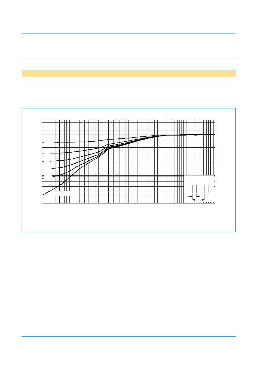
Fig 1.
Normalized total power dissipation as a
function of heatsink temperature.
Fig 2.
Normalized continuous drain current as a
function of heatsink temperature.
T
h
= 25
�
C; I
DM
is single pulse; V
GS
= 10 V.
Fig 3.
Safe operating area; continuous and peak drain currents as a function of drain-source voltage.
03aa13
0
40
80
120
0
50
100
150
200
T
h
(
�
C)
P
der
(%)
03aa21
0
40
80
120
0
50
100
150
200
T
h
(
�
C)
I
der
(%)
P
der
P
tot
P
tot 25 C
�
(
)
-----------------------
100%
�
=
I
der
I
D
I
D 25 C
�
(
)
-------------------
100%
�
=
03ao49
10
-1
1
10
10
2
1
10
10
2
10
3
VDS (V)
ID
(A)
DC
100
�
s
10 ms
Limit RDSon = VDS
/ ID
1 ms
tp = 10
�
s
Philips Semiconductors
PHX23NQ11T
N-channel TrenchMOSTM standard level FET
Product data
Rev. 01 -- 14 May 2004
4 of 12
9397 750 13177
� Koninklijke Philips Electronics N.V. 2004. All rights reserved.
5.
Thermal characteristics
[1]
External heatsink, connected to mounting base.
5.1 Transient thermal impedance
Table 4:
Thermal characteristics
Symbol Parameter
Conditions
Min
Typ
Max
Unit
R
th(j-h)
thermal resistance from junction to heatsink
Figure 4
[1]
-
-
3
K/W
Fig 4.
Transient thermal impedance from junction to heatsink as a function of pulse duration.
03ao48
10-2
10-1
1
10
10-5
10-4
10-3
10-2
10-1
1
10
tp (s)
Zth(j-h)
(K/W)
single pulse
= 0.5
0.2
0.1
0.05
0.02
tp
tp
T
P
t
T
=

Philips Semiconductors
PHX23NQ11T
N-channel TrenchMOSTM standard level FET
Product data
Rev. 01 -- 14 May 2004
5 of 12
9397 750 13177
� Koninklijke Philips Electronics N.V. 2004. All rights reserved.
6.
Characteristics
Table 5:
Characteristics
T
j
= 25
�
C unless otherwise specified.
Symbol Parameter
Conditions
Min
Typ
Max
Unit
Static characteristics
V
(BR)DSS
drain-source breakdown voltage
I
D
= 250
�
A; V
GS
= 0 V
T
j
= 25
�
C
110
-
-
V
T
j
=
-
55
�
C
100
-
-
V
V
GS(th)
gate-source threshold voltage
I
D
= 1 mA; V
DS
= V
GS
;
Figure 9
and
10
T
j
= 25
�
C
2
3
4
V
T
j
= 150
�
C
1
-
-
V
T
j
=
-
55
�
C
-
-
4.4
V
I
DSS
drain-source leakage current
V
DS
= 100 V; V
GS
= 0 V
T
j
= 25
�
C
-
-
10
�
A
T
j
= 150
�
C
-
-
500
�
A
I
GSS
gate-source leakage current
V
GS
=
�
10 V; V
DS
= 0 V
-
10
100
nA
R
DSon
drain-source on-state resistance
V
GS
= 10 V; I
D
= 13 A;
Figure 7
and
8
T
j
= 25
�
C
-
49
70
m
T
j
= 150
�
C
-
132
189
m
Dynamic characteristics
Q
g(tot)
total gate charge
I
D
= 23 A; V
DD
= 80 V; V
GS
= 10 V;
Figure 13
-
22
-
nC
Q
gs
gate-source charge
-
5
-
nC
Q
gd
gate-drain (Miller) charge
-
10
-
nC
C
iss
input capacitance
V
GS
= 0 V; V
DS
= 25 V; f = 1 MHz;
Figure 11
-
830
-
pF
C
oss
output capacitance
-
140
-
pF
C
rss
reverse transfer capacitance
-
85
-
pF
t
d(on)
turn-on delay time
V
DD
= 50 V; R
L
= 2.2
;
V
GS
= 10 V; R
G
= 5.6
-
8
-
ns
t
r
rise time
-
39
-
ns
t
d(off)
turn-off delay time
-
26
-
ns
t
f
fall time
-
24
-
ns
Source-drain diode
V
SD
source-drain (diode forward) voltage I
S
= 11 A; V
GS
= 0 V;
Figure 12
-
0.9
1.5
V
t
rr
reverse recovery time
I
S
= 11 A; dI
S
/dt =
-
100 A/
�
s; V
GS
= 0 V
-
64
-
ns
Q
r
recovered charge
-
120
-
nC

Philips Semiconductors
PHX23NQ11T
N-channel TrenchMOSTM standard level FET
Product data
Rev. 01 -- 14 May 2004
6 of 12
9397 750 13177
� Koninklijke Philips Electronics N.V. 2004. All rights reserved.
T
j
= 25
�
C
T
j
= 25
�
C and 150
�
C; V
DS
>
I
D
x R
DSon
Fig 5.
Output characteristics: drain current as a
function of drain-source voltage; typical values.
Fig 6.
Transfer characteristics: drain current as a
function of gate-source voltage; typical values.
T
j
= 25
�
C
Fig 7.
Drain-source on-state resistance as a function
of drain current; typical values.
Fig 8.
Normalized drain-source on-state resistance
factor as a function of junction temperature.
03ao52
0
5
10
15
20
0
0.5
1
1.5
2
VDS (V)
ID
(A)
4.6 V
Tj = 25
�
C
VGS = 10 V
4.8 V
5 V
5.2 V
8 V
4.4 V
5.4 V
6 V
03ao54
0
5
10
15
20
0
2
4
6
VGS (V)
ID
(A)
VDS > ID x RDSon
Tj = 25
�
C
150
�
C
03ao53
0
0.05
0.1
0.15
0.2
0
5
10
15
20
ID (A)
RDSon
(
)
VGS = 10 V
Tj = 25
�
C
6 V
8 V
4.8 V
5.2 V
5.4 V
5 V
4.6 V
03aa29
0
1
2
3
-60
0
60
120
180
T
j
(
�
C)
a
a
R
DSon
R
DSon 25 C
�
(
)
-----------------------------
=
Philips Semiconductors
PHX23NQ11T
N-channel TrenchMOSTM standard level FET
Product data
Rev. 01 -- 14 May 2004
7 of 12
9397 750 13177
� Koninklijke Philips Electronics N.V. 2004. All rights reserved.
I
D
= 1 mA; V
DS
= V
GS
T
j
= 25
�
C; V
DS
= 5 V
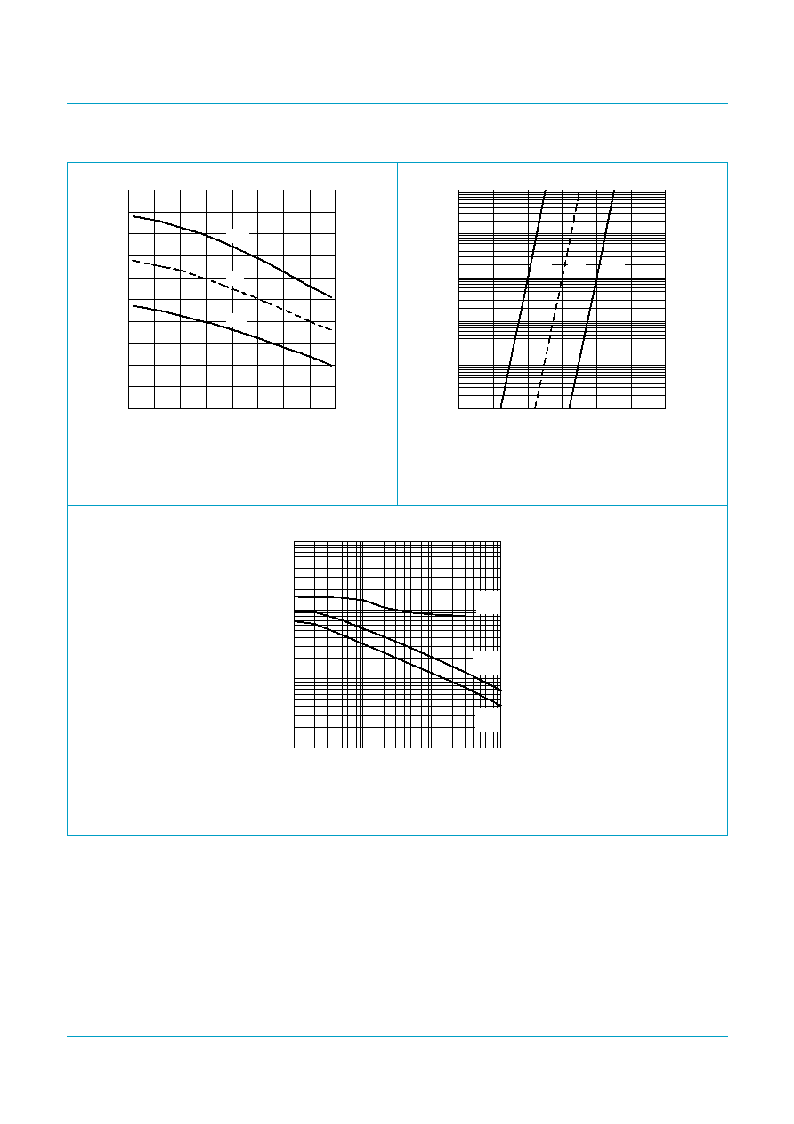
Fig 9.
Gate-source threshold voltage as a function of
junction temperature.
Fig 10. Sub-threshold drain current as a function of
gate-source voltage.
V
GS
= 0 V; f = 1 MHz
Fig 11. Input, output and reverse transfer capacitances as a function of drain-source voltage; typical values.
03aa32
0
1
2
3
4
5
-60
0
60
120
180
T
j
(
�
C)
V
GS(th)
(V)
max
min
typ
03aa35
10
-6
10
-5
10
-4
10
-3
10
-2
10
-1
0
2
4
6
V
GS
(V)
I
D
(A)
max
typ
min
03ao56
10
102
103
104
10-1
1
10
102
VDS (V)
C
(pF)
Ciss
Coss
Crss

Philips Semiconductors
PHX23NQ11T
N-channel TrenchMOSTM standard level FET
Product data
Rev. 01 -- 14 May 2004
8 of 12
9397 750 13177
� Koninklijke Philips Electronics N.V. 2004. All rights reserved.
7.
Isolation characteristics
T
j
= 25
�
C and 150
�
C; V
GS
= 0 V
I
D
= 23 A; V
DD
= 20 V and 80 V
Fig 12. Source (diode forward) current as a function of
source-drain (diode forward) voltage; typical
values.
Fig 13. Gate-source voltage as a function of gate
charge; typical values.
03ao55
0
5
10
15
20
0
0.3
0.6
0.9
1.2
VSD (V)
ID
(A)
Tj = 25
�
C
175
�
C
VGS = 0 V
03ao57
0
5
10
15
0
10
20
30
40
QG (nC)
VGS
(V)
ID = 23 A
Tj = 25
�
C
VDD = 20 V
80 V
Table 6:
Isolation characteristics
Symbol
Parameter
Conditions
Min.
Typ.
Max.
Unit
V
isol
RMS isolation voltage from all three
terminals to external heatsink.
f = 50-60 Hz; sinusoidal waveform;
RH
65%; clean and dust-free.
-
-
2500 V
C
isol
Capacitance from pin 2 (drain) to
external heatsink.
f = 1 MHz
-
10
-
pF

Philips Semiconductors
PHX23NQ11T
N-channel TrenchMOSTM standard level FET
Product data
Rev. 01 -- 14 May 2004
9 of 12
9397 750 13177
� Koninklijke Philips Electronics N.V. 2004. All rights reserved.
8.
Package outline
Fig 14. SOT186A (TO-220F).
REFERENCES
OUTLINE
VERSION
EUROPEAN
PROJECTION
ISSUE DATE
IEC
JEDEC
JEITA
SOT186A
3-lead TO-220F
0
5
10 mm
scale
Plastic single-ended package; isolated heatsink mounted;
1 mounting hole; 3 lead TO-220 'full pack'
SOT186A
A
A1
Q
c
K
j
Notes
1. Terminal dimensions within this zone are uncontrolled. Terminals in this zone are not tinned.
2. Both recesses are
2.5
�
0.8 max. depth
D
D1
L
L2
L1
b1
b2
e1
e
b
w
M
1
2
3
q
E
P
T
UNIT
D
b1
D1
e
q
Q
P
L
c
L2
(1)
max.
e1
A
5.08
3
mm
4.6
4.0
A1
2.9
2.5
b
0.9
0.7
1.1
0.9
b2
1.4
1.0
0.7
0.4
15.8
15.2
6.5
6.3
E
10.3
9.7
2.54
14.4
13.5
T
(2)
2.5
0.4
L1
3.30
2.79
j
2.7
1.7
K
0.6
0.4
2.6
2.3
3.0
2.6
w
3.2
3.0
DIMENSIONS (mm are the original dimensions)
02-03-12
02-04-09
mounting
base

Philips Semiconductors
PHX23NQ11T
N-channel TrenchMOSTM standard level FET
Product data
Rev. 01 -- 14 May 2004
10 of 12
9397 750 13177
� Koninklijke Philips Electronics N.V. 2004. All rights reserved.
9.
Revision history
Table 7:
Revision history
Rev Date
CPCN
Description
01
20040514
-
Product data (9397 750 13177)

9397 750 13177
Philips Semiconductors
PHX23NQ11T
N-channel TrenchMOSTM standard level FET
� Koninklijke Philips Electronics N.V. 2004. All rights reserved.
Product data
Rev. 01 -- 14 May 2004
11 of 12
9397 750 13177
Philips Semiconductors
PHX23NQ11T
N-channel TrenchMOSTM standard level FET
� Koninklijke Philips Electronics N.V. 2004. All rights reserved.
Product data
Rev. 01 -- 14 May 2004
11 of 12
Contact information
For additional information, please visit http://www.semiconductors.philips.com.
For sales office addresses, send e-mail to: sales.addresses@www.semiconductors.philips.com.
Fax: +31 40 27 24825
10. Data sheet status
[1]
Please consult the most recently issued data sheet before initiating or completing a design.
[2]
The product status of the device(s) described in this data sheet may have changed since this data sheet was published. The latest information is available on the Internet at
URL http://www.semiconductors.philips.com.
[3]
For data sheets describing multiple type numbers, the highest-level product status determines the data sheet status.
11. Definitions
Short-form specification -- The data in a short-form specification is
extracted from a full data sheet with the same type number and title. For
detailed information see the relevant data sheet or data handbook.
Limiting values definition -- Limiting values given are in accordance with
the Absolute Maximum Rating System (IEC 60134). Stress above one or
more of the limiting values may cause permanent damage to the device.
These are stress ratings only and operation of the device at these or at any
other conditions above those given in the Characteristics sections of the
specification is not implied. Exposure to limiting values for extended periods
may affect device reliability.
Application information -- Applications that are described herein for any
of these products are for illustrative purposes only. Philips Semiconductors
make no representation or warranty that such applications will be suitable for
the specified use without further testing or modification.
12. Disclaimers
Life support -- These products are not designed for use in life support
appliances, devices, or systems where malfunction of these products can
reasonably be expected to result in personal injury. Philips Semiconductors
customers using or selling these products for use in such applications do so
at their own risk and agree to fully indemnify Philips Semiconductors for any
damages resulting from such application.
Right to make changes -- Philips Semiconductors reserves the right to
make changes in the products - including circuits, standard cells, and/or
software - described or contained herein in order to improve design and/or
performance. When the product is in full production (status `Production'),
relevant changes will be communicated via a Customer Product/Process
Change Notification (CPCN). Philips Semiconductors assumes no
responsibility or liability for the use of any of these products, conveys no
licence or title under any patent, copyright, or mask work right to these
products, and makes no representations or warranties that these products are
free from patent, copyright, or mask work right infringement, unless otherwise
specified.
13. Trademarks
TrenchMOS -- is a trademark of Koninklijke Philips Electronics N.V.
Level
Data sheet status
[1]
Product status
[2][3]
Definition
I
Objective data
Development
This data sheet contains data from the objective specification for product development. Philips
Semiconductors reserves the right to change the specification in any manner without notice.
II
Preliminary data
Qualification
This data sheet contains data from the preliminary specification. Supplementary data will be published
at a later date. Philips Semiconductors reserves the right to change the specification without notice, in
order to improve the design and supply the best possible product.
III
Product data
Production
This data sheet contains data from the product specification. Philips Semiconductors reserves the
right to make changes at any time in order to improve the design, manufacturing and supply. Relevant
changes will be communicated via a Customer Product/Process Change Notification (CPCN).

� Koninklijke Philips Electronics N.V. 2004.
Printed in The Netherlands
All rights are reserved. Reproduction in whole or in part is prohibited without the prior
written consent of the copyright owner.
The information presented in this document does not form part of any quotation or
contract, is believed to be accurate and reliable and may be changed without notice. No
liability will be accepted by the publisher for any consequence of its use. Publication
thereof does not convey nor imply any license under patent- or other industrial or
intellectual property rights.
Date of release: 14 May 2004
Document order number: 9397 750 13177
Contents
Philips Semiconductors
PHX23NQ11T
N-channel TrenchMOSTM standard level FET
1
Product profile . . . . . . . . . . . . . . . . . . . . . . . . . . 1
1.1
Description . . . . . . . . . . . . . . . . . . . . . . . . . . . . 1
1.2
Features . . . . . . . . . . . . . . . . . . . . . . . . . . . . . . 1
1.3
Applications . . . . . . . . . . . . . . . . . . . . . . . . . . . 1
1.4
Quick reference data. . . . . . . . . . . . . . . . . . . . . 1
2
Pinning information . . . . . . . . . . . . . . . . . . . . . . 1
3
Ordering information . . . . . . . . . . . . . . . . . . . . . 2
4
Limiting values. . . . . . . . . . . . . . . . . . . . . . . . . . 2
5
Thermal characteristics. . . . . . . . . . . . . . . . . . . 4
5.1
Transient thermal impedance . . . . . . . . . . . . . . 4
6
Characteristics . . . . . . . . . . . . . . . . . . . . . . . . . . 5
7
Isolation characteristics . . . . . . . . . . . . . . . . . . 8
8
Package outline . . . . . . . . . . . . . . . . . . . . . . . . . 9
9
Revision history . . . . . . . . . . . . . . . . . . . . . . . . 10
10
Data sheet status . . . . . . . . . . . . . . . . . . . . . . . 11
11
Definitions . . . . . . . . . . . . . . . . . . . . . . . . . . . . 11
12
Disclaimers . . . . . . . . . . . . . . . . . . . . . . . . . . . . 11
13
Trademarks. . . . . . . . . . . . . . . . . . . . . . . . . . . . 11