
1.
General description
The SA58631 is a one channel audio amplifier in an HVSON8 package. It provides power
output of 3 W with an 8
load at 9 V supply. The internal circuit is comprised of a BTL
(Bridge Tied Load) amplifier with a complementary PNP-NPN output stage and
standby/mute logic. The SA58631 is housed in an 8-pin HVSON package which has an
exposed die attach paddle enabling reduced thermal resistance and increased power
dissipation.
2.
Features
s
Low junction-to-ambient thermal resistance using exposed die attach paddle
s
Gain can be fixed with external resistors from 6 dB to 30 dB
s
Standby mode controlled by CMOS-compatible levels
s
Low standby current < 10
�
A
s
No switch-on/switch-off plops
s
High power supply ripple rejection: 50 dB minimum
s
ElectroStatic Discharge (ESD) protection
s
Output short circuit to ground protection
s
Thermal shutdown protection
3.
Applications
s
Professional and amateur mobile radio
s
Portable consumer products: toys and games
s
Personal computer remote speakers
SA58631
3 W BTL audio amplifier
Rev. 01 -- 8 March 2006
Product data sheet

SA58631_1
� Koninklijke Philips Electronics N.V. 2006. All rights reserved.
Product data sheet
Rev. 01 -- 8 March 2006
2 of 20
Philips Semiconductors
SA58631
3 W BTL audio amplifier
4.
Quick reference data
[1]
With a load connected at the outputs the quiescent current will increase, the maximum of this increase
being equal to the DC output offset voltage divided by R
L
.
[2]
Supply voltage ripple rejection is measured at the output with a source impedance of R
s
= 0
at the input.
The ripple voltage is a sine wave with a frequency of 1 kHz and an amplitude of 100 mV (RMS), which is
applied to the positive supply rail.
[3]
Supply voltage ripple rejection is measured at the output, with a source impedance of R
s
= 0
at the input.
The ripple voltage is a sine wave with a frequency between 100 Hz and 20 kHz and an amplitude of
100 mV (RMS), which is applied to the positive supply rail.
5.
Ordering information
Table 1:
Quick reference data
V
CC
= 5 V; T
amb
= 25
�
C; R
L
= 8
; f = 1 kHz; V
MODE
= 0 V; measured in test circuit
Figure 3
; unless
otherwise specified.
Symbol
Parameter
Conditions
Min
Typ
Max
Unit
V
CC
supply voltage
operating
2.2
9
18
V
I
q
quiescent current
R
L
=
[1]
-
8
12
mA
I
stb
standby current
V
MODE
= V
CC
-
-
10
�
A
P
o
output power
THD+N = 10 %
1
1.2
-
W
THD+N = 0.5 %
0.6
0.9
-
W
THD+N = 10 %;
V
CC
= 9 V
-
3.0
-
W
THD+N
total harmonic distortion-plus-noise P
o
= 0.5 W
-
0.15
0.3
%
PSRR
power supply rejection ratio
[2]
50
-
-
dB
[3]
40
-
-
dB
Table 2:
Ordering information
Type
number
Package
Name
Description
Version
SA58631TK
HVSON8
plastic thermal enhanced very thin small outline package;
no leads; 8 terminals; body 4 x 4 x 0.85 mm
SOT909-1
SA58631_1
� Koninklijke Philips Electronics N.V. 2006. All rights reserved.
Product data sheet
Rev. 01 -- 8 March 2006
3 of 20
Philips Semiconductors
SA58631
3 W BTL audio amplifier
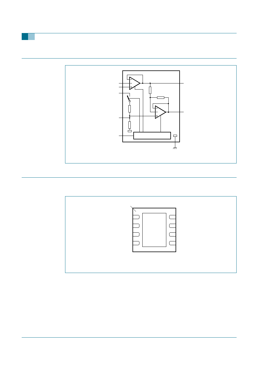
6.
Block diagram
7.
Pinning information
7.1 Pinning
Fig 1.
Block diagram of SA58631
SA58631
V
CC
OUT
-
IN+
IN
-
GND
SVR
OUT+
002aac005
MODE
4
3
6
R
20 k
20 k
2
1
5
STANDBY/MUTE LOGIC
8
7
R
Fig 2.
Pin configuration for HVSON8
002aac006
OUT
-
IN
-
V
CC
IN+
GND
SVR
OUT+
MODE
Transparent top view
5
4
6
3
7
2
8
1
terminal 1
index area
SA58631TK

SA58631_1
� Koninklijke Philips Electronics N.V. 2006. All rights reserved.
Product data sheet
Rev. 01 -- 8 March 2006
4 of 20
Philips Semiconductors
SA58631
3 W BTL audio amplifier
7.2 Pin description
8.
Functional description
The SA58631 is a single-channel BTL audio amplifier capable of delivering 3 W output
power to an 8
load at THD+N = 10 % using a 9 V power supply. Using the MODE pin,
the device can be switched to standby and mute condition. The device is protected by an
internal thermal shutdown protection mechanism. The gain can be set within a range of
6 dB to 30 dB by external feedback resistors.
8.1 Power amplifier
The power amplifier is a Bridge Tied Load (BTL) amplifier with a complementary
PNP-NPN output stage. The voltage loss on the positive supply line is the saturation
voltage of a PNP power transistor, on the negative side the saturation voltage of an NPN
power transistor. The total voltage loss is < 1 V. With a supply voltage of 9 V and an 8
loudspeaker, an output power of 3 W can be delivered to the load.
8.2 Mode select pin (MODE)
The device is in Standby mode (with a very low current consumption) if the voltage at the
MODE pin is greater than V
CC
-
0.5 V, or if this pin is floating. At a MODE voltage in the
range between 1.5 V and V
CC
-
1.5 V the amplifier is in a mute condition. The mute
condition is useful to suppress plop noise at the output, caused by charging of the input
capacitor.
Table 3:
Pin description
Symbol
Pin
Description
MODE
1
operating mode select (standby, mute, operating)
SVR
2
half supply voltage, decoupling ripple rejection
IN+
3
positive input
IN
-
4
negative input
OUT
-
5
negative output terminal
V
CC
6
supply voltage
GND
7
ground
OUT+
8
positive output terminal

SA58631_1
� Koninklijke Philips Electronics N.V. 2006. All rights reserved.
Product data sheet
Rev. 01 -- 8 March 2006
5 of 20
Philips Semiconductors
SA58631
3 W BTL audio amplifier
9.
Limiting values
[1]
AC and DC short-circuit safe voltage.
10. Thermal characteristics
[1]
Thermal resistance is 28 K/W with DAP soldered to
32 cm
2
(5 in
2
)
, 35
�
m copper (1 ounce copper) heat
spreader.
Table 4:
Limiting values
In accordance with the Absolute Maximum Rating System (IEC 60134).
Symbol
Parameter
Conditions
Min
Max
Unit
V
CC
supply voltage
operating
-
0.3
+18
V
V
I
input voltage
-
0.3
V
CC
+ 0.3
V
I
ORM
repetitive peak output current
-
1
A
T
stg
storage temperature
non-operating
-
55
+150
�
C
T
amb
ambient temperature
operating
-
40
+85
�
C
V
P(sc)
short-circuit supply voltage
[1]
-
10
V
P
tot
total power dissipation
HVSON8
-
2.3
W
Table 5:
Thermal characteristics
Symbol
Parameter
Conditions
Typ
Unit
R
th(j-a)
thermal resistance from junction to
ambient
free air
80
K/W
9.7 cm
2
(1.5 in
2
)
heat spreader
[1]
32
K/W
32 cm
2
(5 in
2
)
heat spreader
[1]
28
K/W
R
th(j-sp)
thermal resistance from junction to
solder point
5
K/W

SA58631_1
� Koninklijke Philips Electronics N.V. 2006. All rights reserved.
Product data sheet
Rev. 01 -- 8 March 2006
6 of 20
Philips Semiconductors
SA58631
3 W BTL audio amplifier
11. Static characteristics
[1]
With a load connected at the outputs the quiescent current will increase, the maximum of this increase being equal to the DC output
offset voltage divided by R
L
.
[2]
The DC output voltage with respect to ground is approximately 0.5
�
V
CC
.
12. Dynamic characteristics
[1]
Gain of the amplifier is 2
�
(R2 / R1) in test circuit of
Figure 3
.
[2]
The noise output voltage is measured at the output in a frequency range from 20 Hz to 20 kHz (unweighted), with a source impedance
of R
S
= 0
at the input.
[3]
Supply voltage ripple rejection is measured at the output with a source impedance of R
s
= 0
at the input. The ripple voltage is a
sine wave with a frequency of 1 kHz and an amplitude of 100 mV (RMS), which is applied to the positive supply rail.
[4]
Supply voltage ripple rejection is measured at the output, with a source impedance of R
s
= 0
at the input. The ripple voltage is a
sine wave with a frequency between 100 Hz and 20 kHz and an amplitude of 100 mV (RMS), which is applied to the positive supply rail.
[5]
Output voltage in mute position is measured with an input voltage of 1 V (RMS) in a bandwidth of 20 kHz, which includes noise.
Table 6:
Static characteristics
V
CC
= 5 V; T
amb
= 25
�
C; R
L
= 8
; V
MODE
= 0 V; measured in test circuit
Figure 3
; unless otherwise specified.
Symbol
Parameter
Conditions
Min
Typ
Max
Unit
V
CC
supply voltage
operating
2.2
9
18
V
I
q
quiescent current
R
L
=
[1]
-
8
12
mA
I
stb
standby current
V
MODE
= V
CC
-
-
10
�
A
V
O
output voltage
[2]
-
2.2
-
V
V
O(offset)
differential output voltage offset
-
-
50
mV
I
IB(IN+)
input bias current on pin IN+
-
-
500
nA
I
IB(IN
-
)
input bias current on pin IN
-
-
-
500
nA
V
MODE
voltage on pin MODE
operating
0
-
0.5
V
mute
1.5
-
V
CC
-
1.5
V
standby
V
CC
-
0.5
-
V
CC
V
I
MODE
current on pin MODE
0 V < V
MODE
< V
CC
-
-
20
�
A
Table 7:
Dynamic characteristics
V
CC
= 5 V; T
amb
= 25
�
C; R
L
= 8
; f = 1 kHz; V
MODE
= 0 V; measured in test circuit
Figure 3
; unless otherwise specified.
Symbol
Parameter
Conditions
Min
Typ
Max
Unit
P
o
output power
THD+N = 10 %
1
1.2
-
W
THD+N = 0.5 %
0.6
0.9
-
W
THD+N = 10 %; V
CC
= 9 V
-
3.0
-
W
THD+N
total harmonic distortion
plus noise
P
o
= 0.5 W
-
0.15
0.3
%
G
v(cl)
closed-loop voltage gain
[1]
6
-
30
dB
Z
i
differential input
impedance
-
100
-
k
V
n(o)
noise output voltage
[2]
-
-
100
�
V
PSRR
power supply rejection
ratio
[3]
50
-
-
dB
[4]
40
-
-
dB
V
O
output voltage
mute condition
[5]
-
-
200
�
V
SA58631_1
� Koninklijke Philips Electronics N.V. 2006. All rights reserved.
Product data sheet
Rev. 01 -- 8 March 2006
7 of 20
Philips Semiconductors
SA58631
3 W BTL audio amplifier
13. Application information
14. Test information
14.1 Test conditions
The junction to ambient thermal resistance, R
th(j-a)
= 27.7 K/W for the HVSON8 package
when the exposed die attach paddle is soldered to 32 cm
2
(5 in
2
) area of 35
�
m (1 ounce)
copper heat spreader on the demo PCB. The maximum sine wave power dissipation for
T
amb
= 25
�
C is:
Thus, for T
amb
= +85
�
C the maximum total power dissipation is:
The power dissipation versus ambient temperature curve (
Figure 5
) shows the power
derating profiles with ambient temperature for three sizes of heat spreaders. For a more
modest heat spreader using 9.7 cm
2
(1.5 in
2
) area on the top side of the PCB, the
R
th(j-a)
is 31.25 K/W. When the package is not soldered to a heat spreader, the R
th(j-a)
increases to 83.3 K/W.
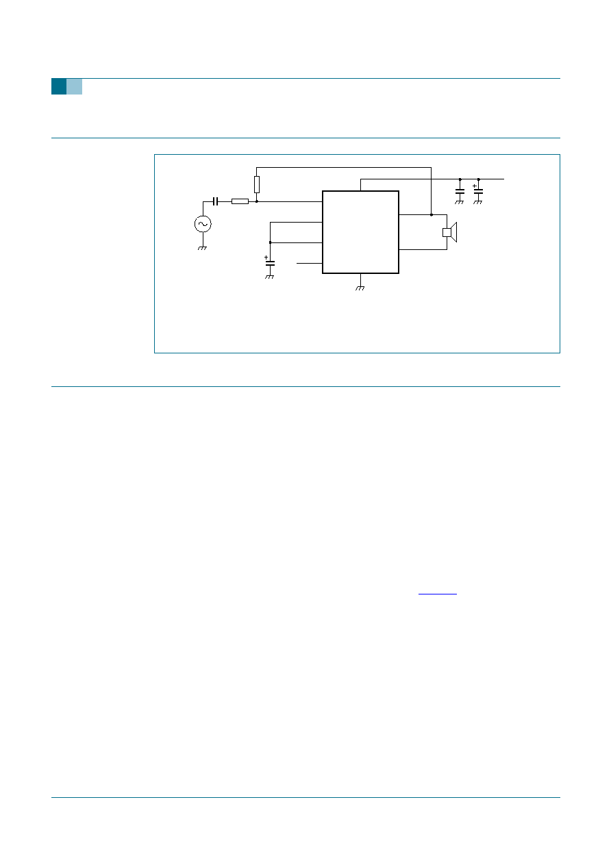
Fig 3.
Application diagram of SA58631 BTL differential output configuration
002aac007
R2
56 k
SA58631
OUT
-
IN+
IN
-
GND
SVR
OUT+
MODE
7
4
3
2
1
5
8
6
C2
47
�
F
R1
11 k
C1
1
�
F
VI
RL
100
�
F
100 nF
V
CC
Gain
2
R2
R1
-------
�
=
150
25
�
27.7
---------------------
4.5 W
=
150
85
�
27.7
---------------------
2.35 W
=

SA58631_1
� Koninklijke Philips Electronics N.V. 2006. All rights reserved.
Product data sheet
Rev. 01 -- 8 March 2006
8 of 20
Philips Semiconductors
SA58631
3 W BTL audio amplifier
14.2 BTL application
T
amb
= 25
�
C, V
CC
= 9 V, f = 1 kHz, R
L
= 8
, G
v
= 20 dB, audio band-pass 20 Hz to
20 kHz. The BTL diagram is shown in
Figure 3
.
The quiescent current has been measured without any load impedance. The total
harmonic distortion + noise (THD+N) as a function of frequency was measured with a
low-pass filter of 80 kHz. The value of capacitor C2 influences the behavior of PSRR at
low frequencies; increasing the value of C2 increases the performance of PSRR.
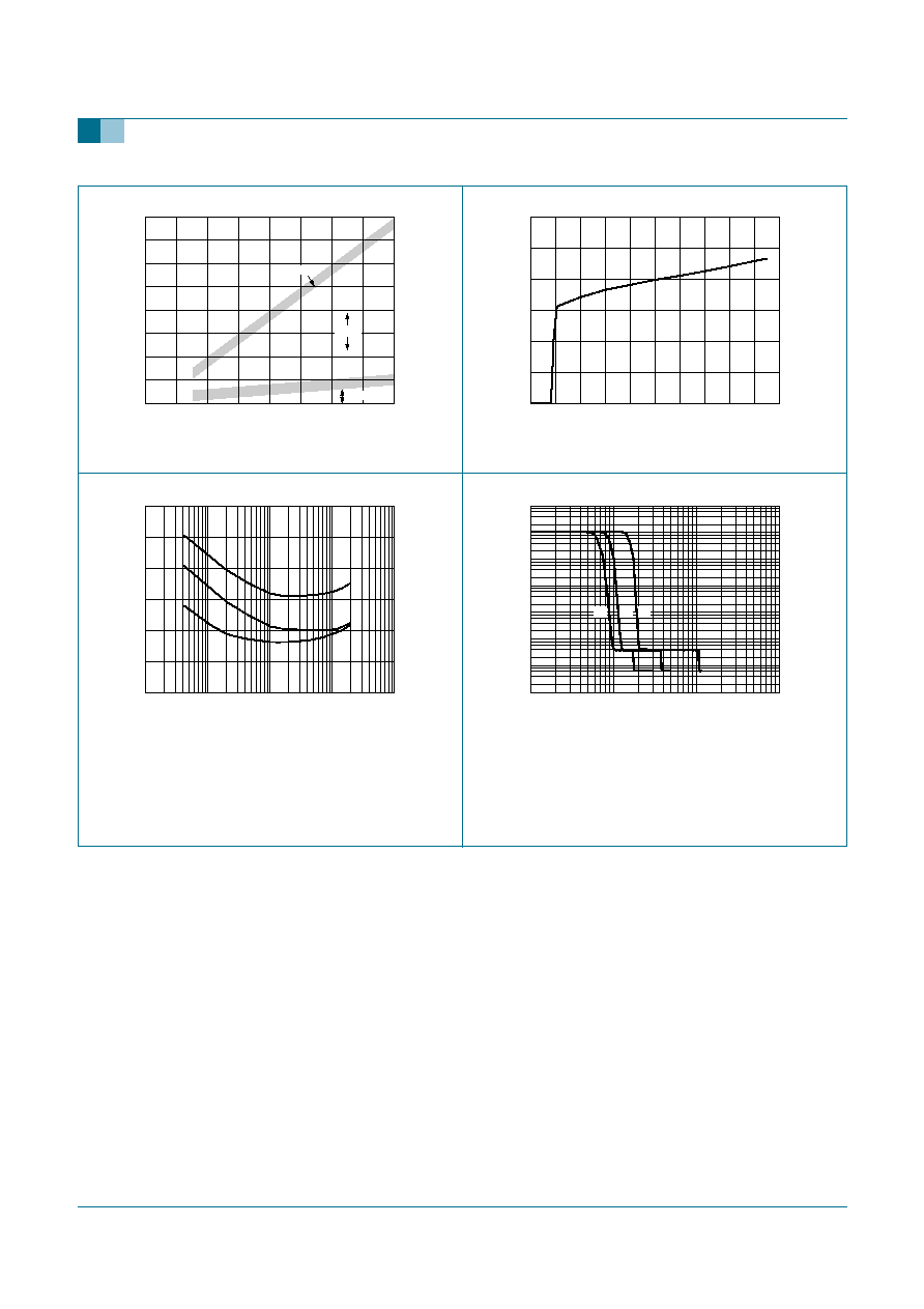
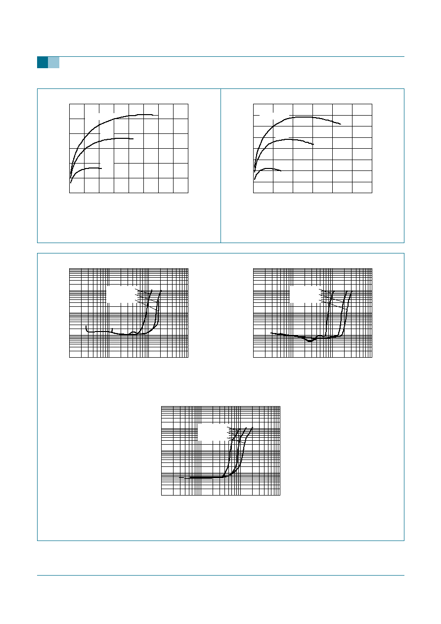
Figure 6
shows three areas: operating, mute and standby. It shows that the DC switching levels of
the mute and standby respectively depends on the supply voltage level.
The following characterization curves show the room temperature performance for
SA58631 using the demo PCB shown in
Figure 21
. The 8 curves for power dissipation
versus output power (
Figure 10
through
Figure 17
) as a function of supply voltage, heat
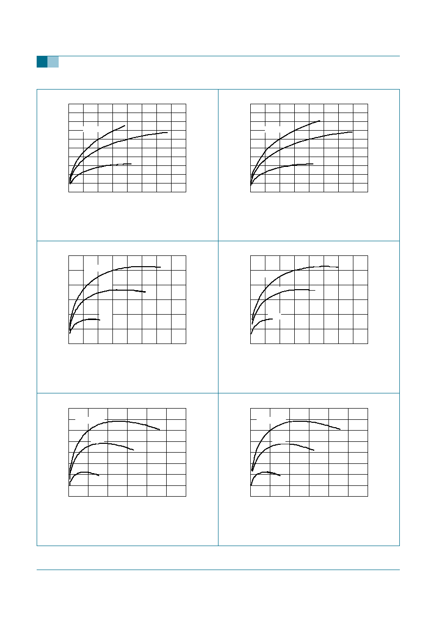
spreader area, load resistance and voltage gain show that there is very little difference in
performance with voltage gain; however, there are significant differences with supply
voltage and load resistance.
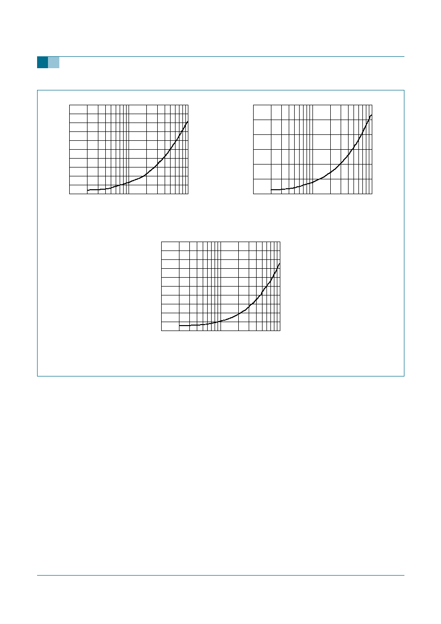
The curves for THD+N versus output power (
Figure 18
) show that the SA58631 yields the
best power output using an 8
load at 9 V supply. Under these conditions the part
delivers typically 3 W output power for THD+N = 10 %.
(1) No heat spreader.
(2) Top only heat spreader (9.7 cm
2
(1.5 in
2
), 35
�
m
(1 ounce) copper).
(3) Both top and bottom heat spreader (approximately
32 cm
2
(5 in
2
), 35
�
m (1 ounce) copper).
Fig 4.
Output power versus supply voltage @
THD+N = 10 %; 32 cm
2
(5 in
2
) heat spreader
Fig 5.
Power dissipation versus ambient temperature
2.0
4.0
6.0
P
o
(W)
0
V
CC
(V)
0
20.0
15.0
5.0
10.0
002aac008
R
L
= 8
W
16
W
002aac009
T
amb
(
�
C)
0
150
100
50
2.0
3.0
1.0
4.0
5.0
P
(W)
0
(1)
(2)
(3)
SA58631_1
� Koninklijke Philips Electronics N.V. 2006. All rights reserved.
Product data sheet
Rev. 01 -- 8 March 2006
9 of 20
Philips Semiconductors
SA58631
3 W BTL audio amplifier
Fig 6.
V
MODE
versus V
CC
Fig 7.
I
q
versus V
CC
V
CC
= 5 V, R
L
= 8
; R
s
= 0
; V
I
= 100 mV.
(1) G
v
= 30 dB
(2) G
v
= 20 dB
(3) G
v
= 6 dB
Band-pass = 22 Hz to 22 kHz.
(1) V
CC
= 3 V
(2) V
CC
= 5 V
(3) V
CC
= 12 V
Fig 8.
SVRR versus frequency
Fig 9.
V
o
versus V
MODE
0
12
8
4
16
V
MODE
(V)
V
CC
(V)
0
16
12
4
8
002aac042
mute
operating
standby
5
10
15
I
q
(mA)
0
V
CC
(V)
0
20
16
8
12
4
002aac043
002aac044
f (Hz)
10
10
5
10
4
10
2
10
3
-
60
-
40
-
20
SVRR
(dB)
-
80
(1)
(2)
(3)
V
MODE
(V)
10
-
1
10
2
10
1
002aac045
(1)
(2) (3)
10
-
6
10
-
5
10
-
4
10
-
3
10
-
2
10
-
1
1
10
V
o
(V)
SA58631_1
� Koninklijke Philips Electronics N.V. 2006. All rights reserved.
Product data sheet
Rev. 01 -- 8 March 2006
10 of 20
Philips Semiconductors
SA58631
3 W BTL audio amplifier
Fig 10. Power dissipation versus output power;
R
L
= 4.0
; G
v
= 10 dB; 9.7 cm
2
(1.5 in
2
)
heat spreader
Fig 11. Power dissipation versus output power;
R
L
= 4.0
; G
v
= 20 dB; 9.7 cm
2
(1.5 in
2
)
heat spreader
Fig 12. Power dissipation versus output power;
R
L
= 8.0
; G
v
= 10 dB; 9.7 cm
2
(1.5 in
2
)
heat spreader
Fig 13. Power dissipation versus output power;
R
L
= 8.0
; G
v
= 20 dB; 9.7 cm
2
(1.5 in
2
)
heat spreader
Fig 14. Power dissipation versus output power;
R
L
= 16
; G
v
= 10 dB; 9.7 cm
2
(1.5 in
2
)
heat spreader
Fig 15. Power dissipation versus output power;
R
L
= 16
; G
v
= 20 dB; 9.7 cm
2
(1.5 in
2
)
heat spreader
2.0
3.0
1.0
4.0
5.0
P
(W)
0
P
o
(W)
0
2.4
1.8
0.6
1.2
002aac027
V
CC
= 9.0 V
7.5 V
5.0 V
2.0
3.0
1.0
4.0
5.0
P
(W)
0
P
o
(W)
0
2.4
1.8
0.6
1.2
002aac028
V
CC
= 9.0 V
7.5 V
5.0 V
1.0
2.0
3.0
P
(W)
0
P
o
(W)
0
4.0
3.0
1.0
2.0
002aac029
V
CC
= 9.0 V
5.0 V
7.5 V
1.0
2.0
3.0
P
(W)
0
P
o
(W)
0
4.0
3.0
1.0
2.0
002aac030
V
CC
= 9.0 V
5.0 V
7.5 V
002aac031
P
o
(W)
0
3.0
2.0
1.0
0
1.2
0.8
0.4
1.6
P
(W)
V
CC
= 9.0 V
5.0 V
7.5 V
002aac032
P
o
(W)
0
3.0
2.0
1.0
0
1.2
0.8
0.4
1.6
P
(W)
V
CC
= 9.0 V
5.0 V
7.5 V
SA58631_1
� Koninklijke Philips Electronics N.V. 2006. All rights reserved.
Product data sheet
Rev. 01 -- 8 March 2006
11 of 20
Philips Semiconductors
SA58631
3 W BTL audio amplifier
Fig 16. Power dissipation versus output power;
R
L
= 8.0
; G
v
= 20 dB; 32 cm
2
(5 in
2
)
heat spreader
Fig 17. Power dissipation versus output power;
R
L
= 16
; G
v
= 20 dB; 32 cm
2
(5 in
2
)
heat spreader
1.0
2.0
3.0
P
(W)
0
P
o
(W)
0
4.0
3.0
1.0
2.0
002aac033
V
CC
= 9.0 V
5.0 V
7.5 V
002aac034
P
o
(W)
0
3.0
2.0
1.0
0
1.2
0.8
0.4
1.6
P
(W)
V
CC
= 9.0 V
5.0 V
7.5 V
a. f = 1 kHz; R
L
= 4
b. f = 1 kHz; R
L
= 8
c. f = 1 kHz; R
L
= 16
Fig 18. THD+N versus output power
002aac035
P
o
(W)
10
-
2
10
1
1
10
-
1
10
-
1
1
10
1
10
2
THD+N
(%)
10
-
2
V
CC
= 5.0 V
9.0 V
7.5 V
002aac036
P
o
(W)
10
-
2
10
1
1
10
-
1
10
-
1
1
10
1
10
2
THD+N
(%)
10
-
2
V
CC
= 5.0 V
9.0 V
7.5 V
10
-
2
10
-
1
10
-
1
1
10
1
10
2
10
-
2
002aac037
P
o
(W)
10
1
1
THD+N
(%)
V
CC
= 5.0 V
9.0 V
7.5 V
SA58631_1
� Koninklijke Philips Electronics N.V. 2006. All rights reserved.
Product data sheet
Rev. 01 -- 8 March 2006
12 of 20
Philips Semiconductors
SA58631
3 W BTL audio amplifier
a. R
L
= 4
b. R
L
= 8
c. R
L
= 16
Fig 19. THD+N versus frequency
002aac038
f (kHz)
10
-
1
10
1
1
0.8
1.2
0.4
1.6
2.0
THD+N
(%)
0
002aac039
f (kHz)
10
-
1
10
1
1
0.4
0.8
1.2
THD+N
(%)
0
002aac040
f (kHz)
10
-
1
10
1
1
0.4
0.6
0.2
0.8
1.0
THD+N
(%)
0
SA58631_1
� Koninklijke Philips Electronics N.V. 2006. All rights reserved.
Product data sheet
Rev. 01 -- 8 March 2006
13 of 20
Philips Semiconductors
SA58631
3 W BTL audio amplifier
14.3 Single-ended application
T
amb
= 25
�
C; V
CC
= 7.5 V; f = 1 kHz; R
L
= 8
; G
v
= 20 dB; audio band-pass 20 Hz to
20 kHz.
The Single-Ended (SE) application diagram is shown in
Figure 20
.
The capacitor value of C3 in combination with the load impedance determines the low
frequency behavior. The total harmonic distortion + noise as a function of frequency was
measured with a low-pass filter of 80 kHz. The value of the capacitor C2 influences the
behavior of the PSRR at low frequencies; increasing the value of C2 increases the
performance of PSRR.
14.4 General remarks
The frequency characteristics can be adapted by connecting a small capacitor across the
feedback resistor. To improve the immunity of HF radiation in radio circuit applications, a
small capacitor can be connected in parallel with the feedback resistor (56 k
); this
creates a low-pass filter.
Fig 20. SE application circuit configuration
002aac041
R2
110 k
SA58631
OUT
-
IN+
IN
-
GND
SVR
OUT+
MODE
7
4
3
2
1
5
8
6
C2
47
�
F
R1
11 k
C1
1
�
F
VI
RL
100
�
F
100 nF
V
CC
C3
470
�
F
Gain
R2
R1
-------
=
SA58631_1
� Koninklijke Philips Electronics N.V. 2006. All rights reserved.
Product data sheet
Rev. 01 -- 8 March 2006
14 of 20
Philips Semiconductors
SA58631
3 W BTL audio amplifier
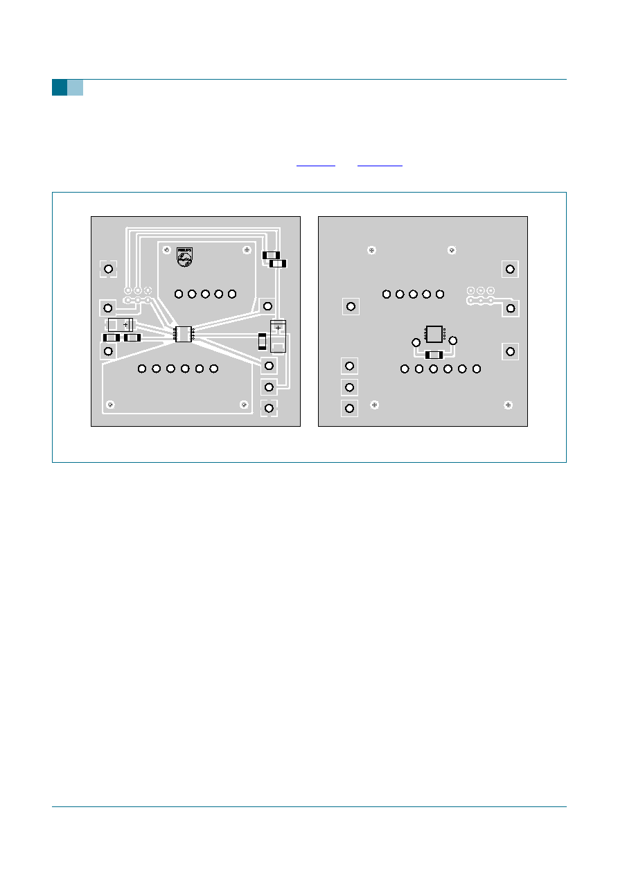
14.5 SA58631TK PCB demo
The application demo board may be used for evaluation in either BTL or SE configuration
as shown in the schematics in
Figure 3
and
Figure 20
. The demo PCB is laid out for the
37 cm
2
(5 in
2
) heat spreader (total of top and bottom heat spreader area).
Fig 21. SA58631TK PCB demo
top layer
bottom layer
SA58631TK
Rev3
100
�
F
11 k
P1
GND
MS
V
CC
V
CC
/2
GND
INPUT
002aac047
6.8 k
6.8 k
100 nF
OUT+
1
�
F
47
�
F
OUT
-
GND
V
CC
SA58631_1
� Koninklijke Philips Electronics N.V. 2006. All rights reserved.
Product data sheet
Rev. 01 -- 8 March 2006
15 of 20
Philips Semiconductors
SA58631
3 W BTL audio amplifier
15. Package outline
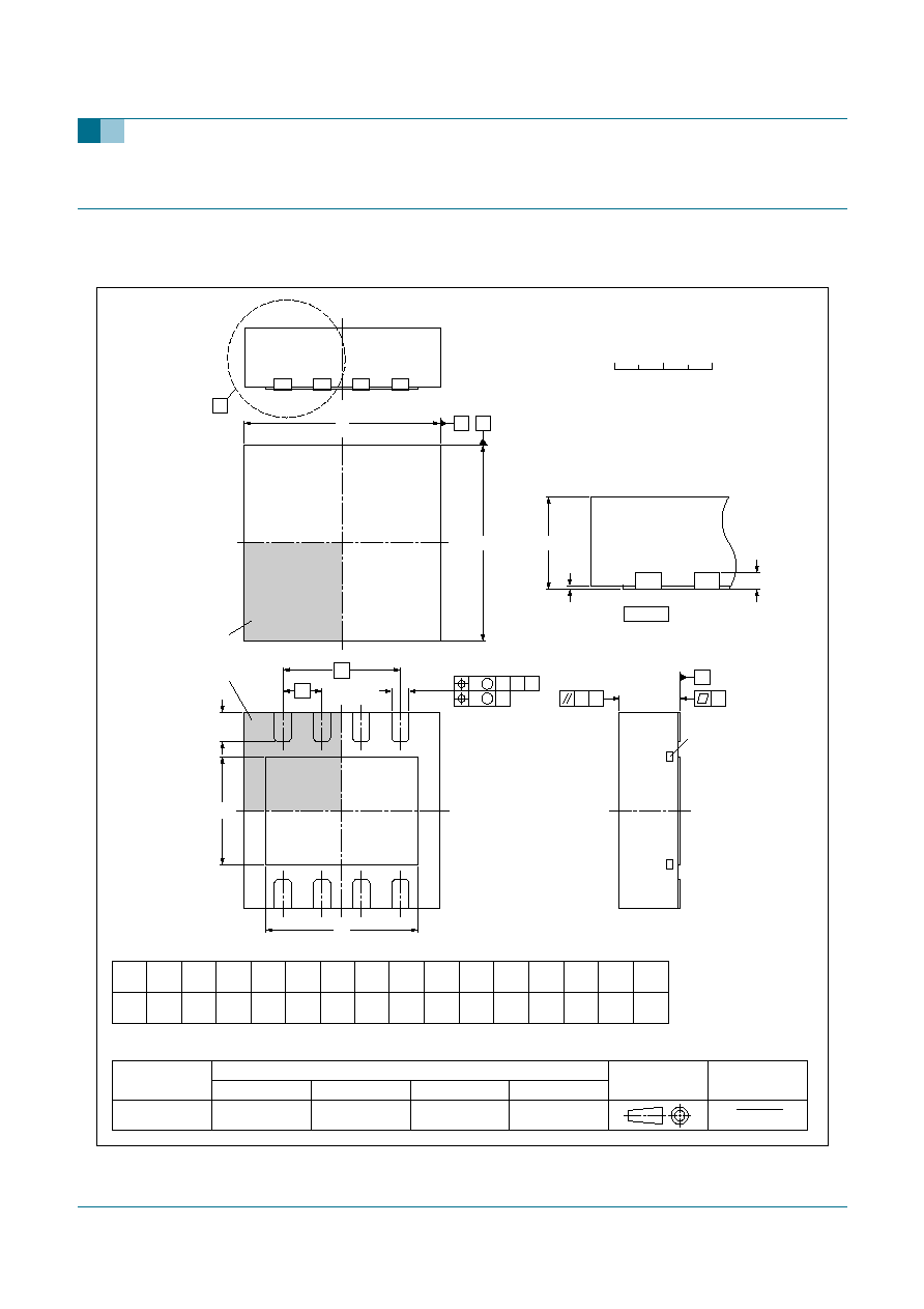
Fig 22. Package outline SOT909-1 (HVSON8)
0.8
0.2
1
0.05
0.00
A1
Eh
b
UNIT
D
(1)
y
e
2.4
e1
REFERENCES
OUTLINE
VERSION
EUROPEAN
PROJECTION
ISSUE DATE
IEC
JEDEC
JEITA
mm
4.1
3.9
c
Dh
2.35
2.05
y1
4.1
3.9
3.25
2.95
0.4
0.3
0.05
0.1
DIMENSIONS (mm are the original dimensions)
SOT909-1
MO-229
E
(1)
0.65
0.40
L
0.1
v
0.05
w
0
2 mm
1
scale
SOT909-1
HVSON8: plastic thermal enhanced very thin small outline package; no leads;
8 terminals; body 4 x 4 x 0.85 mm
A
(1)
max.
05-09-26
05-09-28
Note
1. Plastic or metal protrusions of 0.075 mm maximum per side are not included.
b
terminal 1
index area
terminal 1
index area
C
B
A
e
1
e
A
C
B
v
M
C
w
M
y
C
y
1
X
E
h
D
h
L
1
4
5
8
D
E
detail X
A
A
1
c
exposed tie bar (4
�
)

SA58631_1
� Koninklijke Philips Electronics N.V. 2006. All rights reserved.
Product data sheet
Rev. 01 -- 8 March 2006
16 of 20
Philips Semiconductors
SA58631
3 W BTL audio amplifier
16. Soldering
16.1 Introduction to soldering surface mount packages
This text gives a very brief insight to a complex technology. A more in-depth account of
soldering ICs can be found in our
Data Handbook IC26; Integrated Circuit Packages
(document order number 9398 652 90011).
There is no soldering method that is ideal for all surface mount IC packages. Wave
soldering can still be used for certain surface mount ICs, but it is not suitable for fine pitch
SMDs. In these situations reflow soldering is recommended.
16.2 Reflow soldering
Reflow soldering requires solder paste (a suspension of fine solder particles, flux and
binding agent) to be applied to the printed-circuit board by screen printing, stencilling or
pressure-syringe dispensing before package placement. Driven by legislation and
environmental forces the worldwide use of lead-free solder pastes is increasing.
Several methods exist for reflowing; for example, convection or convection/infrared
heating in a conveyor type oven. Throughput times (preheating, soldering and cooling)
vary between 100 seconds and 200 seconds depending on heating method.
Typical reflow peak temperatures range from 215
�
C to 270
�
C depending on solder paste
material. The top-surface temperature of the packages should preferably be kept:
�
below 225
�
C (SnPb process) or below 245
�
C (Pb-free process)
� for all BGA, HTSSON..T and SSOP..T packages
� for packages with a thickness
2.5 mm
� for packages with a thickness < 2.5 mm and a volume
350 mm
3
so called
thick/large packages.
�
below 240
�
C (SnPb process) or below 260
�
C (Pb-free process) for packages with a
thickness < 2.5 mm and a volume < 350 mm
3
so called small/thin packages.
Moisture sensitivity precautions, as indicated on packing, must be respected at all times.
16.3 Wave soldering
Conventional single wave soldering is not recommended for surface mount devices
(SMDs) or printed-circuit boards with a high component density, as solder bridging and
non-wetting can present major problems.
To overcome these problems the double-wave soldering method was specifically
developed.
If wave soldering is used the following conditions must be observed for optimal results:
�
Use a double-wave soldering method comprising a turbulent wave with high upward
pressure followed by a smooth laminar wave.
�
For packages with leads on two sides and a pitch (e):
� larger than or equal to 1.27 mm, the footprint longitudinal axis is preferred to be
parallel to the transport direction of the printed-circuit board;

SA58631_1
� Koninklijke Philips Electronics N.V. 2006. All rights reserved.
Product data sheet
Rev. 01 -- 8 March 2006
17 of 20
Philips Semiconductors
SA58631
3 W BTL audio amplifier
� smaller than 1.27 mm, the footprint longitudinal axis must be parallel to the
transport direction of the printed-circuit board.
The footprint must incorporate solder thieves at the downstream end.
�
For packages with leads on four sides, the footprint must be placed at a 45
�
angle to
the transport direction of the printed-circuit board. The footprint must incorporate
solder thieves downstream and at the side corners.
During placement and before soldering, the package must be fixed with a droplet of
adhesive. The adhesive can be applied by screen printing, pin transfer or syringe
dispensing. The package can be soldered after the adhesive is cured.
Typical dwell time of the leads in the wave ranges from 3 seconds to 4 seconds at 250
�
C
or 265
�
C, depending on solder material applied, SnPb or Pb-free respectively.
A mildly-activated flux will eliminate the need for removal of corrosive residues in most
applications.
16.4 Manual soldering
Fix the component by first soldering two diagonally-opposite end leads. Use a low voltage
(24 V or less) soldering iron applied to the flat part of the lead. Contact time must be
limited to 10 seconds at up to 300
�
C.
When using a dedicated tool, all other leads can be soldered in one operation within
2 seconds to 5 seconds between 270
�
C and 320
�
C.
16.5 Package related soldering information
[1]
For more detailed information on the BGA packages refer to the
(LF)BGA Application Note (AN01026);
order a copy from your Philips Semiconductors sales office.
[2]
All surface mount (SMD) packages are moisture sensitive. Depending upon the moisture content, the
maximum temperature (with respect to time) and body size of the package, there is a risk that internal or
external package cracks may occur due to vaporization of the moisture in them (the so called popcorn
effect). For details, refer to the Drypack information in the
Data Handbook IC26; Integrated Circuit
Packages; Section: Packing Methods.
[3]
These transparent plastic packages are extremely sensitive to reflow soldering conditions and must on no
account be processed through more than one soldering cycle or subjected to infrared reflow soldering with
peak temperature exceeding 217
�
C
�
10
�
C measured in the atmosphere of the reflow oven. The package
body peak temperature must be kept as low as possible.
Table 8:
Suitability of surface mount IC packages for wave and reflow soldering methods
Package
[1]
Soldering method
Wave
Reflow
[2]
BGA, HTSSON..T
[3]
, LBGA, LFBGA, SQFP,
SSOP..T
[3]
, TFBGA, VFBGA, XSON
not suitable
suitable
DHVQFN, HBCC, HBGA, HLQFP, HSO, HSOP,
HSQFP, HSSON, HTQFP, HTSSOP, HVQFN,
HVSON, SMS
not suitable
[4]
suitable
PLCC
[5]
, SO, SOJ
suitable
suitable
LQFP, QFP, TQFP
not recommended
[5] [6]
suitable
SSOP, TSSOP, VSO, VSSOP
not recommended
[7]
suitable
CWQCCN..L
[8]
, PMFP
[9]
, WQCCN..L
[8]
not suitable
not suitable

SA58631_1
� Koninklijke Philips Electronics N.V. 2006. All rights reserved.
Product data sheet
Rev. 01 -- 8 March 2006
18 of 20
Philips Semiconductors
SA58631
3 W BTL audio amplifier
[4]
These packages are not suitable for wave soldering. On versions with the heatsink on the bottom side, the
solder cannot penetrate between the printed-circuit board and the heatsink. On versions with the heatsink
on the top side, the solder might be deposited on the heatsink surface.
[5]
If wave soldering is considered, then the package must be placed at a 45
�
angle to the solder wave
direction. The package footprint must incorporate solder thieves downstream and at the side corners.
[6]
Wave soldering is suitable for LQFP, QFP and TQFP packages with a pitch (e) larger than 0.8 mm; it is
definitely not suitable for packages with a pitch (e) equal to or smaller than 0.65 mm.
[7]
Wave soldering is suitable for SSOP, TSSOP, VSO and VSSOP packages with a pitch (e) equal to or larger
than 0.65 mm; it is definitely not suitable for packages with a pitch (e) equal to or smaller than 0.5 mm.
[8]
Image sensor packages in principle should not be soldered. They are mounted in sockets or delivered
pre-mounted on flex foil. However, the image sensor package can be mounted by the client on a flex foil by
using a hot bar soldering process. The appropriate soldering profile can be provided on request.
[9]
Hot bar soldering or manual soldering is suitable for PMFP packages.
17. Abbreviations
18. Revision history
Table 9:
Abbreviations
Acronym
Description
BTL
Bridge Tied Load
CMOS
Complementary Metal Oxide Silicon
DAP
Die Attach Paddle
ESD
ElectroStatic Discharge
NPN
Negative-Positive-Negative
PCB
Printed-Circuit Board
PNP
Positive-Negative-Positive
RMS
Root Mean Squared
THD
Total Harmonic Distortion
Table 10:
Revision history
Document ID
Release date
Data sheet status
Change notice
Doc. number
Supersedes
SA58631_1
20060308
Product data sheet
-
-
-

Philips Semiconductors
SA58631
3 W BTL audio amplifier
SA58631_1
� Koninklijke Philips Electronics N.V. 2006. All rights reserved.
Product data sheet
Rev. 01 -- 8 March 2006
19 of 20
19. Data sheet status
[1]
Please consult the most recently issued data sheet before initiating or completing a design.
[2]
The product status of the device(s) described in this data sheet may have changed since this data sheet was published. The latest information is available on the Internet at
URL http://www.semiconductors.philips.com.
[3]
For data sheets describing multiple type numbers, the highest-level product status determines the data sheet status.
20. Definitions
Short-form specification -- The data in a short-form specification is
extracted from a full data sheet with the same type number and title. For
detailed information see the relevant data sheet or data handbook.
Limiting values definition -- Limiting values given are in accordance with
the Absolute Maximum Rating System (IEC 60134). Stress above one or
more of the limiting values may cause permanent damage to the device.
These are stress ratings only and operation of the device at these or at any
other conditions above those given in the Characteristics sections of the
specification is not implied. Exposure to limiting values for extended periods
may affect device reliability.
Application information -- Applications that are described herein for any
of these products are for illustrative purposes only. Philips Semiconductors
makes no representation or warranty that such applications will be suitable for
the specified use without further testing or modification.
21. Disclaimers
Life support -- These products are not designed for use in life support
appliances, devices, or systems where malfunction of these products can
reasonably be expected to result in personal injury. Philips Semiconductors
customers using or selling these products for use in such applications do so
at their own risk and agree to fully indemnify Philips Semiconductors for any
damages resulting from such application.
Right to make changes -- Philips Semiconductors reserves the right to
make changes in the products - including circuits, standard cells, and/or
software - described or contained herein in order to improve design and/or
performance. When the product is in full production (status `Production'),
relevant changes will be communicated via a Customer Product/Process
Change Notification (CPCN). Philips Semiconductors assumes no
responsibility or liability for the use of any of these products, conveys no
license or title under any patent, copyright, or mask work right to these
products, and makes no representations or warranties that these products are
free from patent, copyright, or mask work right infringement, unless otherwise
specified.
22. Trademarks
Notice -- All referenced brands, product names, service names and
trademarks are the property of their respective owners.
23. Contact information
For additional information, please visit: http://www.semiconductors.philips.com
For sales office addresses, send an email to: sales.addresses@www.semiconductors.philips.com
Level
Data sheet status
[1]
Product status
[2] [3]
Definition
I
Objective data
Development
This data sheet contains data from the objective specification for product development. Philips
Semiconductors reserves the right to change the specification in any manner without notice.
II
Preliminary data
Qualification
This data sheet contains data from the preliminary specification. Supplementary data will be published
at a later date. Philips Semiconductors reserves the right to change the specification without notice, in
order to improve the design and supply the best possible product.
III
Product data
Production
This data sheet contains data from the product specification. Philips Semiconductors reserves the
right to make changes at any time in order to improve the design, manufacturing and supply. Relevant
changes will be communicated via a Customer Product/Process Change Notification (CPCN).

� Koninklijke Philips Electronics N.V. 2006
All rights are reserved. Reproduction in whole or in part is prohibited without the prior
written consent of the copyright owner. The information presented in this document does
not form part of any quotation or contract, is believed to be accurate and reliable and may
be changed without notice. No liability will be accepted by the publisher for any
consequence of its use. Publication thereof does not convey nor imply any license under
patent- or other industrial or intellectual property rights.
Date of release: 8 March 2006
Document number: SA58631_1
Published in The Netherlands
Philips Semiconductors
SA58631
3 W BTL audio amplifier
24. Contents
1
General description . . . . . . . . . . . . . . . . . . . . . . 1
2
Features . . . . . . . . . . . . . . . . . . . . . . . . . . . . . . . 1
3
Applications . . . . . . . . . . . . . . . . . . . . . . . . . . . . 1
4
Quick reference data . . . . . . . . . . . . . . . . . . . . . 2
5
Ordering information . . . . . . . . . . . . . . . . . . . . . 2
6
Block diagram . . . . . . . . . . . . . . . . . . . . . . . . . . 3
7
Pinning information . . . . . . . . . . . . . . . . . . . . . . 3
7.1
Pinning . . . . . . . . . . . . . . . . . . . . . . . . . . . . . . . 3
7.2
Pin description . . . . . . . . . . . . . . . . . . . . . . . . . 4
8
Functional description . . . . . . . . . . . . . . . . . . . 4
8.1
Power amplifier . . . . . . . . . . . . . . . . . . . . . . . . . 4
8.2
Mode select pin (MODE) . . . . . . . . . . . . . . . . . 4
9
Limiting values. . . . . . . . . . . . . . . . . . . . . . . . . . 5
10
Thermal characteristics. . . . . . . . . . . . . . . . . . . 5
11
Static characteristics. . . . . . . . . . . . . . . . . . . . . 6
12
Dynamic characteristics . . . . . . . . . . . . . . . . . . 6
13
Application information. . . . . . . . . . . . . . . . . . . 7
14
Test information . . . . . . . . . . . . . . . . . . . . . . . . . 7
14.1
Test conditions . . . . . . . . . . . . . . . . . . . . . . . . . 7
14.2
BTL application . . . . . . . . . . . . . . . . . . . . . . . . . 8
14.3
Single-ended application . . . . . . . . . . . . . . . . 13
14.4
General remarks . . . . . . . . . . . . . . . . . . . . . . . 13
14.5
SA58631TK PCB demo . . . . . . . . . . . . . . . . . 14
15
Package outline . . . . . . . . . . . . . . . . . . . . . . . . 15
16
Soldering . . . . . . . . . . . . . . . . . . . . . . . . . . . . . 16
16.1
Introduction to soldering surface mount
packages . . . . . . . . . . . . . . . . . . . . . . . . . . . . 16
16.2
Reflow soldering . . . . . . . . . . . . . . . . . . . . . . . 16
16.3
Wave soldering . . . . . . . . . . . . . . . . . . . . . . . . 16
16.4
Manual soldering . . . . . . . . . . . . . . . . . . . . . . 17
16.5
Package related soldering information . . . . . . 17
17
Abbreviations . . . . . . . . . . . . . . . . . . . . . . . . . . 18
18
Revision history . . . . . . . . . . . . . . . . . . . . . . . . 18
19
Data sheet status . . . . . . . . . . . . . . . . . . . . . . . 19
20
Definitions . . . . . . . . . . . . . . . . . . . . . . . . . . . . 19
21
Disclaimers . . . . . . . . . . . . . . . . . . . . . . . . . . . . 19
22
Trademarks. . . . . . . . . . . . . . . . . . . . . . . . . . . . 19
23
Contact information . . . . . . . . . . . . . . . . . . . . 19