 | –≠–ª–µ–∫—Ç—Ä–æ–Ω–Ω—ã–π –∫–æ–º–ø–æ–Ω–µ–Ω—Ç: SAA6752HS | –°–∫–∞—á–∞—Ç—å:  PDF PDF  ZIP ZIP |

DATA SHEET
Product specification
Supersedes data of 2002 Dec 09
2004 Jan 26
INTEGRATED CIRCUITS
SAA6752HS
MPEG-2 video and
MPEG-audio/AC-3 audio encoder
with multiplexer

2004 Jan 26
2
Philips Semiconductors
Product specification
MPEG-2 video and MPEG-audio/AC-3
audio encoder with multiplexer
SAA6752HS
CONTENTS
1
FEATURES
1.1
Video input and preprocessing
1.2
Video compression
1.3
Audio input
1.4
Audio compression
1.5
Stream multiplexer
1.6
Output interface
1.7
Control domain
1.8
Other features
2
GENERAL DESCRIPTION
2.1
General
2.2
Application fields
3
QUICK REFERENCE DATA
4
ORDERING INFORMATION
5
BLOCK DIAGRAM
6
PINNING
7
FUNCTIONAL DESCRIPTION
7.1
System operation
7.2
Digital video input
7.3
Video compression
7.4
Digital audio input
7.5
Audio compression
7.6
SDRAM interface
7.7
Multiplexer
7.8
MPEG stream output port
7.9
Clock generation
7.10
Power control and reset
7.11
I
2
C-bus interface
7.12
Exception handling
8
BOUNDARY SCAN TEST
8.1
Initialization of boundary scan circuit
8.2
Device identification codes
9
I
2
C-BUS CONTROL AND STATUS
REGISTERS
10
LIMITING VALUES
11
THERMAL CHARACTERISTICS
12
CHARACTERISTICS
13
PACKAGE OUTLINE
14
SOLDERING
14.1
Introduction to soldering surface mount
packages
14.2
Reflow soldering
14.3
Wave soldering
14.4
Manual soldering
14.5
Suitability of surface mount IC packages for
wave and reflow soldering methods
15
DATA SHEET STATUS
16
DEFINITIONS
17
DISCLAIMERS
18
PURCHASE OF PHILIPS I
2
C COMPONENTS

2004 Jan 26
3
Philips Semiconductors
Product specification
MPEG-2 video and MPEG-audio/AC-3
audio encoder with multiplexer
SAA6752HS
1
FEATURES
1.1
Video input and preprocessing
∑
Digital YUV input according to
"ITU-R BT.656" (8 bits at
27 MHz) and
"ITU-R BT.601"
∑
Support of enhanced
"ITU-R BT.656" input format
containing decoded VBI data readable via I
2
C-bus;
Closed Caption (CC), Wide Screen Signalling (WSS)
and copyright information with Copy Generation
Management System (CGMS)
∑
Processing of non-broadcast video signals from analog
VCR according to IEC 756
∑
Two video clock input pins for switching two digital video
sources
∑
"ITU-R BT.601" format conversion to 1/2D1, 2/3D1 and
Standard Interchange Format (SIF)
∑
4 : 2 : 2 to 4 : 2 : 0 colour format conversion
∑
Decimation filtering for all format conversions
∑
Adaptive median filter and motion compensated filter for
input noise reduction.
1.2
Video compression
∑
Real-time MPEG-2 encoding compliant to Main Profile
at Main Level (MP@ML) for 625 and 525 interlaced line
systems
∑
Supported resolutions: D1, 2/3D1, 1/2D1 and SIF
∑
IPB frame, IP frame and I frame only encoding
supported at all modes
∑
Supported bit rates: up to 25 Mbit/s I-only encoding;
up to 15 Mbit/s IP-only or IBP encoding.
∑
Variable video bit rate mode for constant picture quality
and constant bit rate mode to gain optimum picture
quality from a fixed channel transfer rate
∑
Access to bit rate control parameters whilst encoding to
support external real-time control algorithms (e.g.
constrained variable bit rate control)
∑
Programmable Group Of Pictures (GOP) structure
∑
Innovative motion estimation with wide search range
∑
Adaptive quantization
∑
Motion compensated noise filter.
1.3
Audio input
∑
Audio inputs: I
2
S format or EIAJ format (16, 18 or
20 bits), master or slave mode at 32, 44.1 and 48 kHz
∑
Two digital I
2
S input ports for selection between two
digital audio sources
∑
Audio clock generation: 256f
s
or 384f
s
(where
f
s
= 48 kHz) locked to video frame rate (if video is
present and locking is enabled)
∑
Sample rate conversion to 48 kHz (locked to video
frame rate if enabled) for slave mode operation in all
modes except Digital Versatile Disc (DVD) compliant
bypass.
1.4
Audio compression
∑
Dolby
Æ
(1)
Digital Consumer Encoding (DDCE) also
known as AC-3
(2)
2 channel audio encoding at
256 kbit/s or 384 kbit/s (only for SAA6752HS/V103)
∑
MPEG-1 layer 2 audio encoding at 256 kbit/s or
384 kbit/s
∑
Input data bypass for Linear Pulse Code Modulation
(LPCM) and compressed audio data [MPEG-1,
MPEG-2, Dolby
Æ
Digital (DD) and Digital Theatre
System (DTS)] according to IEC 61937
∑
Preamble Pc, Preamble Pd and bit stream information
captured for identification of modes during bypass of
compressed audio data for MPEG-1, MPEG-2, DD and
DTS according to IEC 61937
∑
Audio mute via I
2
C-bus control for all modes except
DVD-compliant bypass.
(1) Dolby is a registered trademark of Dolby Laboratories
Licensing Corporation.
(2) AC-3 is a registered trademark of Dolby Laboratories
Licensing Corporation.

2004 Jan 26
4
Philips Semiconductors
Product specification
MPEG-2 video and MPEG-audio/AC-3
audio encoder with multiplexer
SAA6752HS
1.5
Stream multiplexer
∑
Multiplexing of video and audio streams according to the
MPEG-2 systems standard (
"ISO 13818-1")
∑
Generation and output of MPEG-2 Transport Streams
(TS), MPEG-2 Program Streams (PS), Packetized
Elementary Streams (PES) and Elementary Streams
(ES) compliant to the DVD, D-VHS and DVB standards
∑
MPEG time stamp (PTS/DTS/SCR/PCR) generation
and insertion (synchronization)
∑
Insertion of metadata
∑
Optional generation of empty time slots for subsequent
insertion of application specific data packets
∑
Optional insertion of user data in the GOP header and in
the picture header
∑
Optional automatic insertion of Closed Caption data
according to DVD or ATSC standard
∑
Optional generation of transport streams with variable
bit rate.
1.6
Output interface
∑
Parallel interface 8-bit master/slave output
∑
3-state output port
∑
Glueless interfacing with IEEE 1394 chip sets (for
example, PDI 1394 L11)
∑
Data Expansion Bus Interface (DEBI) interface.
1.7
Control domain
∑
All control done via I
2
C-bus
∑
I
2
C-bus slave transceiver up to 400 kbit/s
∑
I
2
C-bus slave address select pin
∑
Host interrupt flag pin.
1.8
Other features
∑
Single external clock or single crystal 27 MHz
∑
Separate 27 MHz system clock output
∑
Interface voltage 3.3 V
∑
TTL compatible digital outputs
∑
Power supply voltage 3.3 and 2.5 V
∑
Boundary Scan Test (BST) supported
∑
Power-down mode
∑
Single SDRAM system memory (16 Mbit@16 bit or
64 Mbit@16 bit).
2
GENERAL DESCRIPTION
2.1
General
Philips Semiconductors' second generation real time
MPEG-2 encoder, the SAA6752HS, is a highly integrated
single-chip audio and video encoding solution with flexible
multiplexing functionality. With our expertise in two critical
areas for consumer video encoding, noise filtering and
motion estimation, we have pushed the boundaries for
video quality even further, providing enhanced quality for
low bit rates and enabling increased recording times for a
given storage capacity. The SAA6752HS will also enable
a key driver for new consumer digital recording
applications and system cost reduction. By integrating all
audio encoding and multiplexing functionality we will be
moving from a three chip to a one chip system, with cost
efficient design and process technology, thus providing a
truly low cost, high quality encoding system.
The SAA6752HS/V104 is intended for customers whose
application does not require the DDCE function.
The SAA6752HS gives significant advantages to
customers developing digital recording applications:
∑
Fast time-to-market and low development
resources. By adding a simple external video input
processor IC, an audio analog-to-digital converter, and
an external SDRAM, analog video and audio sources
are compressed into high quality MPEG-2 video and
MPEG-1 layer 2 or AC-3 audio streams, multiplexed into
a single program or transport stream for simple
connection to various storage media or broadcast
media. Hence, making design effort for our customers a
minimum, as well as removing the need for in-depth
experience in MPEG encoding.
∑
Low system host resources. All video and audio
encoding algorithms and software are run on an internal
MIPS
Æ
(1)
processor. The SAA6752HS only requires a
small amount of communication from the system host
processor to set up and control required encoding
parameters via the I
2
C-bus.
(1) MIPS is a registered trademark of MIPS Technologies.

2004 Jan 26
5
Philips Semiconductors
Product specification
MPEG-2 video and MPEG-audio/AC-3
audio encoder with multiplexer
SAA6752HS
2.2
Application fields
2.2.1
DVD
BASED OPTICAL DISC RECORDERS
(DVD+RW,
DVD-RW, DVD-RAM)
Emerging optical disc based recording systems target to
replace the existing consumer recording (VCR) and
playback (DVD and VCD) products. The first generation
recordable DVD based products will want to maximise
recording times for the 4.7 Gbyte storage capacity. For
these systems the SAA6752HS is critical, with its superior
noise filtering and motion estimation, in enabling high
quality at low bit rates.
Playback compatibility with existing DVD decoding
solutions will also be important, which is why the
SAA6752HS provides Dolby
Æ
digital consumer (AC-3)
audio encoding to allow playback through existing players
implementing DDCE (AC-3) decoding dominant in current
DVD platforms.
The DVD stream is based on MPEG Program Stream
(PS). The SAA6752HS directly outputs MPEG PS
compliant to the DVD standard.
2.2.2
HDD
BASED TIME SHIFT RECORDING
Hard Disc Drive (HDD) based time-shift systems enable
Personalized TV (PTV) functionality, providing consumers
with new powers of control over what and when to watch
broadcast content. With the audio and video content
recorded digitally, identification, search and retrieval
becomes a `no brainer' task as compared to traditional
VCR functionality. Combine this with electronic program
guides and intelligent control, and the PTV can also
analyse the viewers watching habits to search for
programs likely to be of interest and automatically
recorded in anticipation of the viewers preferences.
Since HDD recorders are closed systems, the recording
format stream can be proprietary. The SAA6752HS
flexible multiplexing formats support a number of recording
stream formats for HDD including MPEG Transport
Stream (TS) or MPEG Packetized Elementary Stream
(PES).
2.2.3
D
IGITAL
VCR (DVHS)
RECORDING
A DVHS player records streams based on MPEG
Transport Streams (TS) packed in logical tape tracks. The
SAA6752HS output streams are compliant with DVHS
standard requirements.
2.2.4
V
IDEO EDITING
/
TRANSMISSION
/
SURVEILLANCE
/
CONFERENCING
The SAA6752HS can operate as a stand-alone device in
all the above applications. The SAA6752HS full features
and flexibility allows customers to tailor functionality and
performance to specific application requirements. All
required control settings such as GOP size and bit rate
modes can be selected via the I
2
C-bus.
2004 Jan 26
6
Philips Semiconductors
Product specification
MPEG-2 video and MPEG-audio/AC-3
audio encoder with multiplexer
SAA6752HS
3
QUICK REFERENCE DATA
4
ORDERING INFORMATION
Notes
1. MPEG-2 video and MPEG-audio/AC-3 audio encoder with multiplexer.
2. MPEG-2 video and MPEG-audio encoder with multiplexer, but without AC-3 audio encoder.
3. SAA6752HS/V103 is a replacement of SAA6752HS/V101 with enhanced functionality.
4. SAA6752HS/V104 is a replacement of SAA6752HS/V102 with enhanced functionality.
SYMBOL
PARAMETER
MIN.
TYP.
MAX.
UNIT
V
DDP
digital supply voltage (pad cells)
3.0
3.3
3.6
V
V
DDCO
digital supply voltage (core)
2.3
2.5
2.7
V
V
DDA
analog supply voltage (oscillator and PLL)
2.3
2.5
2.7
V
I
DD(tot)
total analog plus digital supply current
407
453
525
mA
P
tot
total power dissipation
0.95
1.16
1.48
W
f
DCXO
quartz frequency (digital controlled tuning) 27
◊
[1
-
(200
◊
10
-
6
)] 27
27
◊
[1 + (200
◊
10
-
6
)] MHz
f
SDRAM
SDRAM clock frequency
-
108
-
MHz
f
SCL
I
2
C-bus input clock frequency
100
-
400
kHz
B
output bit-rate
1.5
-
25
Mbit/s
V
IH
HIGH-level digital input voltage
1.7
-
3.6
V
V
IL
LOW-level digital input voltage
-
0.5
-
+0.7
V
V
OH
HIGH-level digital output voltage
V
DDP
-
0.4
-
V
DDP
V
V
OL
LOW-level digital output voltage
0
-
0.4
V
T
amb
ambient temperature
0
-
70
∞
C
TYPE NUMBER
PACKAGE
NAME
DESCRIPTION
VERSION
SAA6752HS/V103
(1)(3)
SQFP208 plastic shrink quad flat package; 208 leads (lead length 1.3 mm);
body 28
◊
28
◊
3.4 mm; high stand-off height
SOT316-1
SAA6752HS/V104
(2)(4)

2004
Jan
26
7
Philips Semiconductors
Product specification
MPEG-2 video and MPEG-audio/A
C-3
audio encoder with m
ultiple
x
e
r
SAA6752HS
This text is here in white to force landscape pages to be rotated correctly when browsing through the pdf in the Acrobat reader.This text is here in
_
white to force landscape pages to be rotated correctly when browsing through the pdf in the Acrobat reader.This text is here inThis text is here in
white to force landscape pages to be rotated correctly when browsing through the pdf in the Acrobat reader. white to force landscape pages to be ...
5
BLOCK DIA
GRAM
f
ull pagewidth
MHC128
STREAM
MULTIPEXER
VIDEO
COMPRESSION
RESET
CONTROL
MIPS Æ
CPU
GPIO
RAM
ROM
TAP
STATIC
MEM
DEBUG
ONLY
I
2
C-BUS
I
2
C-bus
PI-bus
host interrupt
reset
boundary scan
SDRAM-INTERFACE
STREAM DOMAIN SCHEDULER
VIDEO
FRONT-END
system
clock
reference
system clock
output
SDRAM
16 Mbit @ 16-bit or 64 Mbit @ 16-bit
audio clock
digital
video
input
digital
audio
input
SYSTEM
CLOCK
REFERENCE
CLOCK
27 MHz
external
clock
MPEG
output
OUTPUT
INTERFACE
AUDIO
COMPRESSION
AUDIO
INTERFACE
ROM
RAM
SAA6752HS
Fig.1 Block diagram.

2004 Jan 26
8
Philips Semiconductors
Product specification
MPEG-2 video and MPEG-audio/AC-3
audio encoder with multiplexer
SAA6752HS
6
PINNING
SYMBOL
PIN
INPUT/OUTPUT
(1)
I
max
(mA)
DESCRIPTION
V
SSP
1
ground
-
pad ground
SDATA1
2
input
-
I
2
S-bus serial data input port 1 with internal pull-down resistor
SCLK1
3
input/output
4
I
2
S-bus serial clock port 1 with internal pull-down resistor
SWS1
4
input/output
4
I
2
S-bus word select port 1 with internal pull-down resistor
V
DDP
5
supply
-
pad ring supply voltage (3.3 V)
SDATA2
6
input/output
4
I
2
S-bus serial data port 2 with internal pull-down resistor
SCLK2
7
input/output
4
I
2
S-bus serial clock port 2 with internal pull-down resistor
SWS2
8
input/output
4
I
2
S-bus word select port 2 with internal pull-down resistor
ACLK
9
output
4
audio clock output (256f
s
or 384f
s
)
V
SSP
10
ground
-
pad ground
IDQ
11
input
-
reserved input with internal pull-down resistor; (recommended
to connect to pin V
SSP
)
YUV0
12
input
-
video input signal bit 0 (LSB)
YUV1
13
input
-
video input signal bit 1
YUV2
14
input
-
video input signal bit 2
YUV3
15
input
-
video input signal bit 3
YUV4
16
input
-
video input signal bit 4
YUV5
17
input
-
video input signal bit 5
YUV6
18
input
-
video input signal bit 6
YUV7
19
input
-
video input signal bit 7 (MSB)
V
SSP
20
ground
-
pad ground
HSYNC
21
input
-
horizontal sync input (video) with internal pull-down resistor
VSYNC
22
input
-
vertical sync input (video) with internal pull-down resistor
FID
23
input
-
video field identification input (odd/even field) with internal
pull-down resistor
VCLK1
24
input
-
video clock input 1 (27 MHz) with internal pull-down resistor
V
SSCO
25
ground
-
core ground
V
SSCO
26
ground
-
core ground
V
DDCO
27
supply
-
core supply voltage (2.5 V)
V
DDCO
28
supply
-
core supply voltage (2.5 V)
V
DDP
29
supply
-
pad ring supply voltage (3.3 V)
VCLK2
30
input
-
video clock input 2 (27 MHz) with internal pull-down resistor
PDOAV
31
3-state output
4
parallel stream data output for audio/video identifier
PDIDS
32
input
-
parallel stream data input for data strobe [request for packet in
Data Expansion Bus Interface (DEBI) slave mode] with internal
pull-up resistor
PDOSYNC
33
3-state output
4
parallel stream data output for packet sync
V
SSP
34
ground
-
pad ground
PDOVAL
35
3-state output
4
parallel stream data valid output with internal pull-up resistor
PDO0
36
3-state output
4
parallel stream data output bit 0 (LSB)

2004 Jan 26
9
Philips Semiconductors
Product specification
MPEG-2 video and MPEG-audio/AC-3
audio encoder with multiplexer
SAA6752HS
PDO1
37
3-state output
4
parallel stream data output bit 1
PDO2
38
3-state output
4
parallel stream data output bit 2
V
DDP
39
supply
-
pad ring supply voltage (3.3 V)
PDO3
40
3-state output
4
parallel stream data output bit 3
PDO4
41
3-state output
4
parallel stream data output bit 4
PDO5
42
3-state output
4
parallel stream data output bit 5
PDO6
43
3-state output
4
parallel stream data output bit 6
V
SSP
44
ground
-
pad ground
PDO7
45
3-state output
4
parallel stream data output bit 7 (MSB)
PDIOCLK
46
input/output
4
parallel stream clock input/output
I2CADDRSEL
47
input
-
I
2
C-bus address select input with internal pull-up resistor
SD_DQ15
48
input/output
8
SDRAM data input/output bit 15 (MSB)
V
DDP
49
supply
-
pad ring supply voltage (3.3 V)
SD_DQ0
50
input/output
8
SDRAM data input/output bit 0 (LSB)
SD_DQ14
51
input/output
8
SDRAM data input/output bit 14
SD_DQ1
52
input/output
8
SDRAM data input/output bit 1
V
SSP
53
ground
-
pad ground
SD_DQ13
54
input/output
8
SDRAM data input/output bit 13
SD_DQ2
55
input/output
8
SDRAM data input/output bit 2
SD_DQ12
56
input/output
8
SDRAM data input/output bit 12
V
DDP
57
supply
-
pad ring supply voltage (3.3 V)
SD_DQ3
58
input/output
8
SDRAM data input/output bit 3
SD_DQ11
59
input/output
8
SDRAM data input/output bit 11
SD_DQ4
60
input/output
8
SDRAM data input/output bit 4
SD_DQ10
61
input/output
8
SDRAM data input/output bit 10
V
SSP
62
ground
-
pad ground
SD_DQ5
63
input/output
8
SDRAM data input/output bit 5
SD_DQ9
64
input/output
8
SDRAM data input/output bit 9
SD_DQ6
65
input/output
8
SDRAM data input/output bit 6
SD_DQ8
66
input/output
8
SDRAM data input/output bit 8
V
DDP
67
supply
-
pad ring supply voltage (3.3 V)
SD_DQ7
68
input/output
8
SDRAM data input/output bit 7
SD_DQM1
69
output
8
SDRAM data mask enable output bit 1
SD_DQM0
70
output
8
SDRAM data mask enable output bit 0 (LSB)
SD_WE
71
output
8
SDRAM write enable output (active LOW)
V
SSP
72
ground
-
pad ground
SD_CAS
73
output
8
SDRAM column address strobe output (active LOW)
SD_CLK
74
output
8
SDRAM clock output
SD_RAS
75
output
8
SDRAM row address strobe output (active LOW)
SD_CKE
76
output
8
SDRAM clock enable output
SYMBOL
PIN
INPUT/OUTPUT
(1)
I
max
(mA)
DESCRIPTION

2004 Jan 26
10
Philips Semiconductors
Product specification
MPEG-2 video and MPEG-audio/AC-3
audio encoder with multiplexer
SAA6752HS
V
SSCO
77
ground
-
core ground
V
SSCO
78
ground
-
core and substrate ground
V
DDCO
79
supply
-
core supply voltage (2.5 V)
V
DDCO
80
supply
-
core supply voltage (2.5 V)
V
DDP
81
supply
-
pad ring supply voltage (3.3 V)
SD_CS
82
output
8
SDRAM chip select output (active LOW)
SD_A13
83
output
8
SDRAM address output bit 13 (bank selection for 64 Mbit)
SD_A9
84
output
8
SDRAM address output bit 9
SD_A8
85
output
8
SDRAM address output bit 8
V
SSP
86
ground
-
pad ground
SD_A11
87
output
8
SDRAM address output bit 11 (bank selection for 16 Mbit)
SD_A7
88
output
8
SDRAM address output bit 7
SD_A12
89
output
8
SDRAM address output bit 12 (bank selection for 64 Mbit)
SD_A6
90
output
8
SDRAM address output bit 6
V
DDP
91
supply
-
pad ring supply voltage (3.3 V)
SD_A10
92
output
8
SDRAM address output bit 10
SD_A5
93
output
8
SDRAM address output bit 5
SD_A0
94
output
8
SDRAM address output bit 0 (LSB)
SD_A4
95
output
8
SDRAM address output bit 4
V
SSP
96
ground
-
pad ground
SD_A1
97
output
8
SDRAM address output bit 1
SD_A3
98
output
8
SDRAM address output bit 3
SD_A2
99
output
8
SDRAM address output bit 2
SD_DQM3
100
output
8
reserved (do not connect)
V
DDP
101
supply
-
pad ring supply voltage (3.3 V)
SD_DQM2
102
output
8
reserved (do not connect)
SD_DQ31
103
input/output
8
reserved (do not connect)
SD_DQ16
104
input/output
8
reserved (do not connect)
V
SSP
105
ground
-
pad ground
SD_DQ30
106
input/output
8
reserved (do not connect)
SD_DQ17
107
input/output
8
reserved (do not connect)
SD_DQ29
108
input/output
8
reserved (do not connect)
V
DDP
109
supply
-
pad ring supply voltage (3.3 V)
SD_DQ18
110
input/output
8
reserved (do not connect)
SD_DQ28
111
input/output
8
reserved (do not connect)
SD_DQ19
112
input/output
8
reserved (do not connect)
SD_DQ27
113
input/output
8
reserved (do not connect)
V
SSP
114
ground
-
pad ground
SD_DQ20
115
input/output
8
reserved (do not connect)
SD_DQ26
116
input/output
8
reserved (do not connect)
SYMBOL
PIN
INPUT/OUTPUT
(1)
I
max
(mA)
DESCRIPTION

2004 Jan 26
11
Philips Semiconductors
Product specification
MPEG-2 video and MPEG-audio/AC-3
audio encoder with multiplexer
SAA6752HS
SD_DQ21
117
input/output
8
reserved (do not connect)
SD_DQ25
118
input/output
8
reserved (do not connect)
V
DDP
119
supply
-
pad ring supply voltage (3.3 V)
SD_DQ22
120
input/output
8
reserved (do not connect)
SD_DQ24
121
input/output
8
reserved (do not connect)
SD_DQ23
122
input/output
8
reserved (do not connect)
EXTCLK
123
input
-
27 MHz external clock input with internal pull-up resistor
V
SSP
124
ground
-
pad ground
V
SSA
125
ground
-
oscillator analog ground
XTALI
126
analog input
-
crystal oscillator input (27 MHz); note 2
XTALO
127
analog output
-
crystal oscillator output (27 MHz)
V
DDA
128
supply
-
oscillator analog supply voltage (2.5 V)
V
SSCO
129
ground
-
core ground
V
SSCO
130
ground
-
core ground
V
DDCO
131
supply
-
core supply voltage (2.5 V)
V
DDCO
132
supply
-
core supply voltage (2.5 V)
V
DDP
133
supply
-
pad ring supply voltage (3.3 V)
TDI
134
input
-
boundary scan test data input; pin must float or set to HIGH
during normal operating; with internal pull-up resistor; note 3
TMS
135
input
-
boundary scan test mode select; pin must float or set to HIGH
during normal operating; with internal pull-up resistor; note 3
TCK
136
input
-
boundary scan test clock; pin must be set to LOW during
normal operating; with internal pull-up resistor; note 3
TDO
137
3-state output
4
boundary scan test data output; pin not active during normal
operating; with 3-state output; note 3
V
SSP
138
ground
-
pad ground
TRST
139
input
-
test reset input (active LOW), for boundary scan test (with
internal pull-up resistor); notes 3 and 4
CLKOUT
140
output
4
27 MHz system clock output
TEST0
141
input/output
4
reserved (do not connect)
TEST1
142
input/output
4
reserved (do not connect)
V
DDP
143
supply
-
pad ring supply voltage (3.3 V)
TEST2
144
input/output
4
reserved (do not connect)
SDA
145
input/open-drain
output
-
I
2
C-bus serial data input/output
SCL
146
input/open-drain
output
-
I
2
C-bus serial clock input/output
RESET
147
input
-
reset input (active LOW); with internal pull-up resistor
V
SSP
148
ground
-
pad ground
RTS
149
output
4
reserved (do not connect); Universal Asynchronous
Receiver/Transmitter (UART) request to send output (active
LOW)
SYMBOL
PIN
INPUT/OUTPUT
(1)
I
max
(mA)
DESCRIPTION

2004 Jan 26
12
Philips Semiconductors
Product specification
MPEG-2 video and MPEG-audio/AC-3
audio encoder with multiplexer
SAA6752HS
CTS
150
input
-
reserved (recommended connect to pin V
DDP
); UART clear to
send input; external static memory select input (active LOW);
with internal pull-up resistor
RXD
151
input
-
reserved (recommended connect to pin V
DDP
); UART receive
data; internal boot select input; with internal pull-up resistor
TXD
152
output
4
reserved (do not connect); UART transmit data
V
DDP
153
supply
-
pad ring supply voltage (3.3 V)
SM_LB
154
input/output
4
reserved (do not connect)
SM_UB
155
input/output
4
reserved (do not connect)
H_IRF
156
3-state output
4
host interrupt flag output; with internal pull-up resistor
(active LOW)
V
SSP
157
ground
-
pad ground
SM_OE
158
output
4
reserved (do not connect); static memory output enable output
(active LOW)
SM_A9
159
output
4
reserved (do not connect); static memory address output bit 9
SM_A10
160
output
4
reserved (do not connect); static memory address output bit 10
V
DDP
161
supply
-
pad ring supply voltage (3.3 V)
SM_A8
162
output
4
reserved (do not connect); static memory address output bit 8
SM_A11
163
output
4
reserved (do not connect); static memory address output bit 11
SM_A7
164
output
4
reserved (do not connect); static memory address output bit 7
SM_A12
165
output
4
reserved (do not connect); static memory address output bit 12
V
SSP
166
ground
-
pad ground
SM_A6
167
output
4
reserved (do not connect); static memory address output bit 6
SM_A13
168
output
4
reserved (do not connect); static memory address output bit 13
SM_A5
169
output
4
reserved (do not connect); static memory address output bit 5
SM_A14
170
output
4
reserved (do not connect); static memory address output bit 14
V
DDP
171
supply
-
pad ring supply voltage (3.3 V)
SM_WE
172
output
4
reserved (do not connect); static memory write enable output
(active LOW)
SM_D7
173
input/output
4
reserved (do not connect); static memory data input/output
bit 7 with internal pull-down resistor
SM_D8
174
input/output
4
reserved (do not connect); static memory data input/output
bit 8 with internal pull-down resistor
SM_D6
175
input/output
4
reserved (do not connect); static memory data input/output
bit 6 with internal pull-down resistor
V
SSP
176
ground
-
pad ground
SM_D9
177
input/output
4
reserved (do not connect); static memory data input/output
bit 9 with internal pull-down resistor
SM_D5
178
input/output
4
reserved (do not connect); static memory data input/output
bit 5 with internal pull-down resistor
SM_D10
179
input/output
4
reserved (do not connect); static memory data input/output
bit 10 with internal pull-down resistor
SYMBOL
PIN
INPUT/OUTPUT
(1)
I
max
(mA)
DESCRIPTION

2004 Jan 26
13
Philips Semiconductors
Product specification
MPEG-2 video and MPEG-audio/AC-3
audio encoder with multiplexer
SAA6752HS
SM_D4
180
input/output
4
reserved (do not connect); static memory data input/output
bit 4 with internal pull-down resistor
V
SSCO
181
ground
-
internal pre-driver and substrate ground
V
SSCO
182
ground
-
core ground
V
DDCO
183
supply
-
core supply voltage (2.5 V)
V
DDCO
184
supply
-
internal pre-driver supply voltage (2.5 V)
V
DDP
185
supply
-
pad ring supply voltage (3.3 V)
SM_D11
186
input/output
4
reserved (do not connect); static memory data input/output
bit 11 with internal pull-down resistor
SM_D3
187
input/output
4
reserved (do not connect); static memory data input/output
bit 3 with internal pull-down resistor
SM_D12
188
input/output
4
reserved (do not connect); static memory data input/output
bit 12 with internal pull-down resistor
SM_D2
189
input/output
4
reserved (do not connect); static memory data input/output
bit 2 with internal pull-down resistor
V
SSP
190
ground
-
pad ground
SM_D13
191
input/output
4
reserved (do not connect); static memory data input/output
bit 13 with internal pull-down resistor
SM_D1
192
input/output
4
reserved (do not connect); static memory data input/output
bit 1 with internal pull-down resistor
SM_D14
193
input/output
4
reserved (do not connect); static memory data input/output
bit 14 with internal pull-down resistor
SM_D0
194
input/output
4
reserved (do not connect); static memory data input/output
bit 0 (LSB) with internal pull-down resistor
V
DDP
195
supply
-
pad ring supply voltage (3.3 V)
SM_D15
196
input/output
4
reserved (do not connect); static memory data input/output
bit 15 (MSB) with internal pull-down resistor
SM_CS3
197
output
4
reserved (do not connect); static memory chip select output for
external ROM or RAM (active LOW)
SM_A4
198
output
4
reserved (do not connect); static memory address output bit 4
SM_A3
199
output
4
reserved (do not connect); static memory address output bit 3
V
SSP
200
ground
-
pad ground
SM_A2
201
output
4
reserved (do not connect); static memory address output bit 2
SM_A15
202
output
4
reserved (do not connect); static memory address output bit 15
SM_A1
203
output
4
reserved (do not connect); static memory address output bit 1
SM_A16
204
output
4
reserved (do not connect); static memory address output bit 16
V
DDP
205
supply
-
pad ring supply voltage (3.3 V)
SM_A0
206
output
4
reserved (do not connect); static memory address output bit 0
(LSB)
SM_A17
207
output
4
reserved (do not connect); static memory address output bit 17
(MSB)
SM_CS0
208
output
4
reserved (do not connect)
SYMBOL
PIN
INPUT/OUTPUT
(1)
I
max
(mA)
DESCRIPTION

2004 Jan 26
14
Philips Semiconductors
Product specification
MPEG-2 video and MPEG-audio/AC-3
audio encoder with multiplexer
SAA6752HS
Notes
1. All input pins, input/output pins (in input mode), output pins (in 3-state mode) and open-drain output pins are limited
to 3.3 V.
2. If used with external clock source the input voltage has to be limited to 2.5 V.
3. In accordance with the
"IEEE 1149.1" standard.
4. Special function of pin TRST:
a) For board designs without boundary scan implementation, pin TRST must be connected to ground.
b) Pin TRST provides easy initialization of the internal BST circuit. By applying a LOW level it can be used to force
the internal Test Access Port (TAP) controller to the Test-Logic-Reset state (normal operating) immediately.
handbook, halfpage
SAA6752HS
1
208
157
53
104
52
156
105
MHC129
Fig.2 Pin configuration.
2004 Jan 26
15
Philips Semiconductors
Product specification
MPEG-2 video and MPEG-audio/AC-3
audio encoder with multiplexer
SAA6752HS
7
FUNCTIONAL DESCRIPTION
7.1
System operation
7.1.1
G
ENERAL
The SAA6752HS has a multi-processor architecture.
The different processing and control modules are not
locked to each other but run independently within the limits
of the global scheduling. The data transfer between the
processing units is carried out via FIFO memories or the
external SDRAM. The device is configured and the
operation modes are selected via the I
2
C-bus.
7.1.2
O
PERATING MODES
There are five operating modes:
1. Idle. This mode is set after applying a hard reset (i.e.
on power-up). In this mode the SAA6752HS can be
initialized by the host to the required configuration.
Video and audio processing is disabled. A hard reset
always resets the SAA6752HS configuration
parameters back to the default states.
2. Stop. In Stop mode, the video and audio input
processing is enabled but the multiplexer output
remains disabled. It is possible to read status
information on the input video and audio signals via
the I
2
C-bus. The SAA6752HS initialization settings
cannot be modified, except to some specific dynamic
encoding parameters (i.e. bit rate setting).
3. Encode. In this mode, the multiplexer output is
enabled. Like Stop mode, only dynamic encoding
parameters can be modified in this mode.
4. Paused. This mode allows the SAA6752HS to make
seamless transitions. Restarting from Paused mode
will generate a stream output with sequential time
stamps and MPEG buffer model content.
5. Power-down. In this mode, the internal clock is
disabled, sending the SAA6752HS into a
(non-functional) power saving state. A hard reset will
re-initialize the SAA6752HS.
handbook, full pagewidth
MHC130
Power-
down
Idle
SLEEP
HARD RESET
HARD RESET
Stop
Encode
Paused
power
applied
RECONFIGURE
RECONFIGURE
ENABLE
STOP
START
START
START
PAUSE
Fig.3 Mode transition diagram.

2004 Jan 26
16
Philips Semiconductors
Product specification
MPEG-2 video and MPEG-audio/AC-3
audio encoder with multiplexer
SAA6752HS
7.1.3
M
ODE TRANSITION COMMANDS
There are seven mode transition commands:
1. SOFT RESET. Like a hard reset, a soft reset can be
applied in any mode, setting the SAA6752HS back to
Idle mode and resetting all configuration parameters
back to the default settings.
2. RECONFIGURE. This command sets the
SAA6752HS back to Idle mode without resetting the
configuration parameters back to the default settings.
3. ENABLE. This transition sets Stop mode, enabling the
video and audio input processing.
4. START. This transition sets Encode mode, enabling
the multiplexer stream output. Note that if the
SAA6752HS is commanded to start from the Idle
mode, then the internal transition is via the Stop mode.
5. STOP. This command will disable the multiplexer
stream output, setting the SAA6752HS to Stop mode.
The current GOP and/or audio frame is completed and
an end of sequence bit appended to the stream.
6. PAUSE. A PAUSE transition will cause the multiplexer
to complete the current GOP and/or audio frame but
no end of sequence bit is appended. The current
MPEG buffer model contents are saved to provide a
seamless transition on START.
7. SLEEP. This mode disables the internal clock.
8. FORCED RECONFIGURE. A STOP command whilst
in the Encode mode will not work in case the video or
audio input signal is interrupted, because for stopping,
the SAA6752HS tries to finish the current GOP. The
forced reconfigure command allows a mode transition
back to the Idle state, without losing the actual
configuration settings. The forced reconfiguration
performs a soft reset and the automatic internal
reprogramming of the I
2
C-bus registers. The forced
reconfiguration will take about 200 ms; during the
forced reconfiguration all register values will change to
their default values before they are reprogrammed.
Please note that outputs, which can be switched to
high-impedance or to input mode, will not be active
during the forced reconfiguration.
The SAA6752HS is not able to process any other
commands during mode transitions. In this event, a get
running mode request will return a busy flag. The
completion of a mode transition can also be flagged as an
event using the host interrupt pin.
7.2
Digital video input
7.2.1
G
ENERAL
The video front-end processes an
"ITU-R BT.601/605"
compliant video stream for conversion to 4 : 2 : 0 format
(MP@ML). It includes synchronization, digital video signal
processing through several filters, subsampling, sliced/raw
VBI data handling, and SDRAM address generation.
The video interface is designed for use with Philips
SAA7114 digital multi-standard decoder or similar video
decoders. The input interface accepts a digital video input
stream according to
"ITU-R-BT.601". 625 lines standard at
50 Hz and 720 pixels by 576 lines as well as 525 lines at
60 Hz and 720 pixels by 480 lines are covered. The video
synchronization may either follow
"ITU-R-BT.656"
recommendation or can also be supplied by external
signals (HSYNC, VSYNC and FID). The formatter module
performs a colour conversion from 4 : 2 : 2 to 4 : 2 : 0
format. Optionally, also SIF progressive downscaling and
2/3D1, 1/2D1 downscaling may be activated.
The SAA6752HS supports non-standard features of the
SAA711x series of video input processors, such as
hard-wired external synchronization signals (2 and 3-wire
sync), special VCR playback signal streams (IEC 756
subset for VCR playback and still pictures), extraction of
sliced data from the input video stream.
7.2.2
V
IDEO FRONT
-
END CONFIGURATION OPTIONS
The following configuration options can be selected from
the host:
∑
VIDEO INPUT PORT SELECTION. Two input clock pins
are selectable.
∑
VIDEO INPUT FORMAT. 525 or 625-line formats can be
selected.
∑
VIDEO SYNC FORMAT. Various combinations and
polarities of HSYNC, VSYNC and Field Information
(FID) can be selected as the source of sync signal
processing.
∑
VIDEO FILTER SETTINGS. Noise pre-filter and
horizontal filters can be enabled and, if the default
coefficients are not suitable for an application, new
coefficients can be set.
∑
VIDEO FORMAT CONVERSION. Selection of
conversion from D1 to 1/2D1, 2/3D1 or SIF progressive
downscaling.
∑
VBI DATA EXTRACTION. VBI data extraction of WSS
or CC data can be enabled.

2004 Jan 26
17
Philips Semiconductors
Product specification
MPEG-2 video and MPEG-audio/AC-3
audio encoder with multiplexer
SAA6752HS
7.2.3
V
IDEO ENCODER STATUS INFORMATION
The following configuration option can be selected from
the host:
∑
VBI DATA: WSS and CC data can be read back via the
I
2
C-bus.
7.2.4
D
ATA INPUT FORMAT
7.2.4.1
Interface definition
The data input interface uses 13 pins, all of which are
inputs (see Table 1). Pins YUV0 to YUV7 carry video and
synchronization data and 3 pins are reserved for control
purposes. Two separate clock inputs allow two different
signal sources to be used. The input clock can be
asynchronous to the SAA6752HS system clock.
Table 1
List of pins data input port
Note
1. In ITU-T 656 mode sync signals are embedded in the
video data input stream. The external sync signals are
not used.
7.2.5
V
IDEO SIGNAL PROCESSING
7.2.5.1
Acquisition of video data
Data is latched with the incoming video clock to provide
robust data capture. Video clock and data is unlocked to
the internal system clock therefore a clock domain bridge
is used. This is performed by oversampling of video clock
and data with 108 MHz.
7.2.5.2
Sync decoding and filtering
To allow selection of the right portion of the video input
stream, synchronization signals from the stream are
recognized by a sync decoder. This checks the incoming
field (FID), vertical sync and horizontal sync. It is possible
to select either `internal synchronization' (which means
that SAV/EAV codes in the ITU 601/656 video streams are
used) or externally applied hardware synchronization
signals (which are given by the video input processor).
In the latter case, 3 pin or 2 pin (V-sync and H-sync only)
synchronization can be used.
Using 2 pin synchronization, the FID information is given
by the timing of the transition of the V-sync. If a Vertical
Blanking Interval (VBI) starts during H-sync, the next field
will be the top field, otherwise it will be the bottom field.
A sync filter is used to inhibit sync signal triggering if an
incorrect number of pixels or lines has been input. It also
checks for the correct consecutive fields. The filter works
on three different levels. An H-sync is only accepted after
a predefined number of video cycles, a V-sync is only
accepted after a programmed number of lines and a field
is only accepted if top field follows bottom field or vice
versa.
7.2.5.3
Horizontal and vertical shift
This function is intended for correction in synchronization
of external sync signals if incorrectly timed. The amount of
shift is programmable via the I
2
C-bus.
7.2.5.4
SAV/EAV decoder
A SAV/EAV decoder extracts the F, V and H bits from the
video timing reference code. The decoder evaluates the
protection bits to be able to correct one bit errors within the
code word. If multiple bit errors are detected, the protection
bits are ignored and the field (F), vertical sync (V) and
horizontal sync (H) bits are directly extracted from the
code.
7.2.5.5
Video format conversion
The SAA6752HS converts the input video input signal to
the formats defined in Table 2 controlled by the I
2
C-bus
command. A 4 : 2 : 2 to 4 : 2 : 0 colour conversion is
performed as this is a pre-requisite of MPEG MP@ML
encoding.
PIN
DESCRIPTION
YUV0 to YUV7
video input signal
(synchronous to VCLK)
FID
odd/even field identification
signal; note 1
HSYNC
horizontal synchronization
signal; note 1
VSYNC
vertical synchronization
signal; note 1
VCLK1 or VCLK2
video clock signal (from
source 1 or 2)

2004 Jan 26
18
Philips Semiconductors
Product specification
MPEG-2 video and MPEG-audio/AC-3
audio encoder with multiplexer
SAA6752HS
Table 2
Format conversion
Notes
1. The 8 pixels at the right edge of the scaled picture are
not encoded.
2. Top field only.
7.2.6
V
IDEO FILTERING
7.2.6.1
Adaptive mean filter
The SAA6752HS uses an adaptive mean filter. There are
three different filter modes that can be selected: median,
averaging or no filter.
The median algorithm provides better noise performance
and is well suited to suppress single noise spikes without
degrading the signal edges. The averaging algorithm is a
standard low-pass filter so has greater impact on signal
edges.
The default threshold and gain coefficients of this filter can
be overwritten via the I
2
C-bus to allow user optimization for
different applications.
7.2.6.2
Horizontal pre-filter/decimation filter
There is a horizontal filter for Y and C and this can operate
as a pre-filter or decimation filter. It is a symmetrical FIR
filter with up to 8 coefficients programmable via the
I
2
C-bus.
7.2.6.3
Vertical chrominance filtering
For 4 : 2 : 2 to 4 : 2 : 0 conversion, vertical filtering and
subsampling of the chrominance is performed. The
sequence of coefficients is mirrored in top and bottom field.
This generates the right phases of the chrominance
samples between the luminance samples (a non co-sited
sampling scheme).
7.2.7
VBI
DATA EXTRACTION
The SAA6752HS supports the extraction of WSS and CC
data using two independent VBI data extractor modules.
The data is available via the I
2
C-bus.
The following VBI data formats are supported: Closed
Caption (CC525 and CC625) and Wide Screen Signalling
(WSS525 and WSS625). For CC525, CC625 and
WSS625 the sliced data from a video input processor (e.g.
SAA7114, SAA7115 or SAA7118) are extracted from the
digital video input signal and can be read via the I
2
C-bus.
For WSS525 an internal data slicer is available which
slices the oversampled raw data, which are delivered by
the video input processor. The extracted WSS525 signal
can be read via the I
2
C-bus.
Optionally the automatic insertion of extracted Closed
Caption data into the user data area of a video stream is
possible (for details see Section 7.3.8).
7.3
Video compression
7.3.1
G
ENERAL
Compression of video data is performed by the video
compressor block; see Fig.4. The input to this block is the
uncompressed video information pre-processed by the
video front-end and stored in external SDRAM memory.
The output is a compressed video stream, compliant to
MPEG-2 Video Elementary Stream (VES) up to slice level.
Controlling information (for example, quantizer step size)
as well as the bit stream for higher layers of the VES is
generated by the embedded MIPS
Æ
processor of the
SAA6752HS.
The video compressor contains several subblocks. The
MacroBlock Processor (MBP) performs generation of
video ES on macroblock level. Controlling parameters for
this task and MB headers as well as slice headers are
generated by the core control subblock. Bitstream
formatting and concatenation of MBP bitstream and
header information is done by the subblocks pre-packer
and packer.
MODE
PICTURE FORMAT
(PIXEL/LINES)
D1
720
2/3D1
480
1/2D1
352; note 1
SIF
352; notes 1 and 2

2004 Jan 26
19
Philips Semiconductors
Product specification
MPEG-2 video and MPEG-audio/AC-3
audio encoder with multiplexer
SAA6752HS
7.3.2
V
IDEO ENCODER CONFIGURATION OPTIONS
The following configuration options can be selected from
the host:
∑
VIDEO COMPRESSION SETTINGS. I, IP and IPB
encoding with various GOP structures can be selected.
∑
ENCODER BIT RATE. The bit rate for variable bit rate
or constant bit rate modes can be programmed using bit
rate and quantization control parameters. These
parameters can be adjusted whilst encoding, not just set
at initialization.
∑
ENCODER PERFORMANCE TUNING. The ability for
the user to tune encoding performance is provided by
allowing control of adaptive quantization depth. Also the
SAA6752HS allows download of new quantizer matrix
contents.
7.3.3
V
IDEO ENCODER STATUS INFORMATION
The following status information is available to the host:
∑
CURRENT ENCODER BIT RATE. The actual encoded
bit rate, as number of bytes per GOP, is available
allowing the use of constrained variable bit rate
algorithms to fine tune the encoding efficiency.
7.3.4
GOP
STRUCTURE
The programmable GOP structure features a reference
frame distance (M) up to 3, and a GOP length (N) of up
to 19. Supported structures are real closed GOP(M,N) and
backward predicted closed GOP(M,N). For the use of
B-frames in D1 and 2/3D1 mode a 64 Mbit SDRAM is
needed.
In D1 mode, B-frames will be unidirectional. Backward
predicted closed GOPs may have the first one (M = 2) or
two (M = 3) B-frames referenced inside the GOP
dependent on the I
2
C-bus register settings. This is
intended for editable applications as GOPs are
independent of each other. Non-editable GOPs allow the
first one (M = 1) or two (M = 2) B-frames to be referenced
to the P-frame in the previous GOP. This is a non-editable
format but has optimum encoding efficiency. This structure
is sometimes called an open GOP. The first one (M = 1) or
two (M = 2) B-frames in the first GOP of a sequence are
always forced backwards predicted.
Table 3
GOP
Notes
1. Undefined.
2. This GOP structure is defined as a Real Closed GOP
(RCG).
3. This GOP structure is defined as a Backward
Predicted Closed GOP (BPCG) or Non-Editable GOP
(NEG), selectable via the I
2
C-bus.
GOP
LENGTH (N)
REFERENCE FRAME DISTANCE (M)
0
1
2
3
1
I
(1)
(1)
(1)
2
(1)
IP
(1)
(1)
3
(1)
IPP
IBP
(2)
(1)
4
(1)
IPPP
BIBP
(3)
IBBP
(2)
5
(1)
IPPPP
IBPBP
(2)
(1)
6
(1)
IPP...PP BIBPBP
(3)
BBIBBP
(3)
7
(1)
IPP...PP IBP...BP
(2)
IBBPBBP
(2)
8
(1)
IPP...PP BIBP...BP
(3)
(1)
9
(1)
IPP...PP IBP...BP
(2)
BBI...BBP
(3)
10
(1)
IPP...PP BIBP...BP
(3)
IBBP...BBP
(2)
11
(1)
IPP...PP IBP...BP
(2)
(1)
12
(1)
IPP...PP BIBP...BP
(3)
BBI...BBP
(3)
13
(1)
IPP...PP IBP...BP
(2)
IBBP...BBP
(2)
14
(1)
IPP...PP BIBP...BP
(3)
(1)
15
(1)
IPP...PP IBP...BP
(2)
BBI...BBP
(3)
16
(1)
IPP...PP BIBP...BP
(3)
IBBP...BBP
(3)
17
(1)
IPP...PP IBP...BP
(2)
(1)
18
(1)
IPP...PP BIBP...BP
(3)
BBI...BBP
(3)
19
(1)
IPP...PP IBP...BP
(2)
IBBP...BBP
(2)

2004 Jan 26
20
Philips Semiconductors
Product specification
MPEG-2 video and MPEG-audio/AC-3
audio encoder with multiplexer
SAA6752HS
7.3.5
B
IT RATE CONTROL
The SAA6752HS supports two modes of video bit rate
control: variable bit rate and constant bit rate.
The Variable Bit Rate (VBR) mode is intended for burst
data transfer applications, where the bit rate is allowed to
vary but the image quality should be constant. In this
mode, a combination of three parameters can be set: Rvbr,
Qmin_VBR and Qmax_VBR. While aiming at the target bit
rate Rvbr, only quantizer scale values within the range
between Qmin_VBR and Qmax_VBR are applied.
Broadening this range leads to greater variations in picture
quality but better adherence to Rmax. Constriction of this
range forces a better constancy in picture quality at the
expense of meeting the target bit rate. Note that optimal
control results require reasonable combinations of Rmax,
Qmin_VBR and Qmax_VBR. Furthermore, the maximum
bit rate Rmax can be set. If Rmax is reached in VBR mode,
the CBR algorithm takes over the control by increasing the
quantizer scale values temporarily (over Qmax_VBR) to
guarantee that Rmax is never exceeded. Hence, the
closer Rmax and Rvbr are chosen, the more the control in
VBR mode turns to CBR mode behaviour.
The Constant Bit Rate (CBR) mode is intended for
applications, where a fixed channel rate is provided (e.g.
transmission systems). A tight control of the quantizer
scale is applied to make optimal use of the given
bandwidth. The parameter Rmax specifies the required
constant bit rate.
Independent of the bit rate mode (CBR or VBR), a B-frame
weighting factor (the weighting factor is applied to the
quantization scale) can be applied to further reduce the
bit rate of B-frames. In IP-only GOP structures, every
second P-frame is weighted by this factor generating
`virtual B-frames' to simulate a bit rate distribution similar
to IPB sequences. This feature can further improve the
perceptual rate-distortion ratio by taking advantage of the
inertia of the human visual system.
7.3.6
A
DAPTIVE QUANTIZATION
Adaptive quantization is an algorithm that uses internal
generated statistics to fine tune the quantizer scale used
for encoding a specific macroblock. For example, the
controller adapts the quantization scale with respect to the
local complexity distribution within a frame, resulting in a
perceptually smoother picture quality. The amount of fine
tuning can be adjusted by control of the adaptive
quantization depth.
7.3.7
Q
UANTIZER MATRIX TABLE DOWNLOAD
The MPEG standard default quantizer matrices can be
overwritten to allow picture encoding optimization.
7.3.8
U
SER DATA INSERTION
User data insertion of up to 64 bytes is supported on GOP
and picture level.
Different modes can be selected via I
2
C-bus.
7.3.8.1
External user data insertion (permanently
repeated)
User data is downloaded via the I
2
C-bus to
subaddresses 73H/76H and the number of inserted user
data bytes is set via subaddresses 74H/75H. In Encode
mode the downloaded user data will be inserted
permanently into the user data area of the video stream.
It is possible to download a new set of user data during
Encode mode. The new data will be repeatedly inserted as
soon as the download is finished. It is possible to stop the
user data insertion with a special command.
7.3.8.2
External user data insertion (each downloaded
byte inserted only once)
In this mode each downloaded user data byte is inserted
only once into the user data area. If no new user data is
downloaded between two GOP or pictures then no user
data will be inserted. This mode can be used to transmit
more than 64 bytes of user data from the encoder to the
decoder, e.g. 1000 bytes distributed on 15 packets of
64 bytes and one packet of 40 bytes. The host has to
control the insertion and repetition of user data. A host
interrupt 'mode transition completed' is signalled, if not
masked and the bit 9 of the exception status word is set
when the user data have been read by the video encoder.
Then new user data can be downloaded via I
2
C-bus.

2004 Jan 26
21
Philips Semiconductors
Product specification
MPEG-2 video and MPEG-audio/AC-3
audio encoder with multiplexer
SAA6752HS
7.3.8.3
Internal Closed Caption user data insertion
compliant to ATSC/NTSC standard
Automatic insertion of Closed Caption data into the user
data 2 area on picture header level compliant to the ATSC
and EIA-708 standard can be selected via the I
2
C-bus.
Closed Caption data, which is delivered from the video
input processor (e.g. SAA7114) and captured in the video
front-end will be inserted into the user data 2 area (picture
header level) of the video stream. Preconditions are
appropriate settings of the video input processor and the
VBI data extractor in the video front-end. The Closed
Caption user data will be written for both fields. If no valid
Closed Caption data for field 2 is available these data will
be marked as invalid in the stream. At SIF mode only
field 1 Closed Captions can be inserted from the video
input signal and dummy values (80H 80H) will be inserted
for field 2.
If extended data services (XDS data, line 21 field 2) are
inserted, the insertion will be transparent. No modification
of the CGMS-A copy information will be done.
In accordance to EIA-708 the Closed Caption data will
appear in the stream in transport order. If B-frames are
present the user data is re-ordered in the same way as the
video frames.
Advanced TV Closed Captioning (ATVCC) channel packet
data (cc_type 10 or 11) is not supported, because the
input signal of the encoder is an analog video signal, which
can carry only NTSC Closed Captions, but not ATV Closed
Captions.
No additional user data on picture header level can be
inserted if internal Closed Caption user data insertion
compliant to the ATSC/NTSC standard is active.
7.3.8.4
Internal Closed Caption user data insertion
compliant to DVD standard
Automatic insertion of Closed Caption data into the user
data area on GOP header level compliant to the DVD
standard can be selected via I
2
C-bus.
Closed Caption data, which is delivered from the video
input processor (e.g. SAA7114) and captured in the video
front-end will be inserted into the user data 1 area (GOP
header level) of the video stream. Preconditions are
appropriate settings of the video input processor and the
VBI data extractor in the video front-end. The Closed
Caption user data will be written for both fields. If no valid
Closed Caption data for field 2 is available these data will
be marked as invalid in the stream.
If extended data services (XDS data, line 21 field 2) are
inserted, the insertion will be transparent. No modification
of the CGMS-A copy information will be done.
The Closed Caption data will be inserted for each field of
the GOP in display order. At SIF mode only field 1 Closed
Captions can be inserted from the video input signal and
dummy values (80H 80H) will be inserted for field 2.
The user data is delayed by one GOP period. The first
GOP in the stream carries dummy data marked as invalid.
No additional user data on GOP header level can be
inserted if internal Closed Caption user data insertion
compliant to the DVD standard is active.
The amount of user data depends on the GOP size:
5 bytes header and 3 bytes/field are required. With the
maximum GOP size of 19 this results in
5 + 19
◊
2
◊
3 = 119 bytes, which is more than the
available array of 64 bytes for GOP user data. Therefore
the 64 byte array for picture user data is also used for GOP
user data, if GOP sizes larger than 9 are selected. Then all
128 bytes, which are available for user data insertion on
GOP and picture header level will be used for the insertion
of CC data on GOP level. In this case no additional user
data insertion on picture header level is possible.
7.3.9
M
OTION ADAPTIVE NOISE REDUCTION
The gain and adaptivity can be controlled to optimize
encoding efficiency in case of noisy input sequences, i.e.
off-air reception.

2004 Jan 26
22
Philips Semiconductors
Product specification
MPEG-2 video and MPEG-audio/AC-3
audio encoder with multiplexer
SAA6752HS
7.3.10
C
OMPRESSION BLOCK PARTITIONING
The video compression block, shown in Fig.4, contains the
following sub-modules:
∑
MacroBlock Processor (MBP). Reads uncompressed
video data from SDRAM and generates the compressed
bitstream on MB level (without MB headers). Addresses
for frame buffer (previous frame) access are generated
by the MBP.
∑
Core control. Performs MB and slice header
generation, base address generation for the current MB
(uncompressed), motion vector candidate generation,
and computation of encoding statistics required by the
CPU for bit rate controlling.
∑
Pre-packer (part of packing unit). Since the MBP output
words are not necessarily fully used (i.e. some output
words may contain unused bits) the pre-packer packs
the output of the MBP in such a way that all words
contain valid bits. This reduces the amount of memory
required for storing the MB data.
∑
Packer (part of packing unit). Merges header and MB
headers.
handbook, full pagewidth
MHC131
PRE-
PACKER
MBP/CPM
CORE CONTROL
GENERIC INTERFACE
to/from PCI-bus
from video
front-end
to/from SDRAM-IF
to SDRAM-IF
MEMORY
PACKING UNIT
VIDEO COMPRESSION BLOCK
PACKER
Fig.4 Video compressor block diagram.

2004 Jan 26
23
Philips Semiconductors
Product specification
MPEG-2 video and MPEG-audio/AC-3
audio encoder with multiplexer
SAA6752HS
7.4
Digital audio input
7.4.1
G
ENERAL
The audio input interface (I
2
S) accepts serial digital audio
data and supports master and slave mode. The interface
is able to handle 16 to 20 bits audio data with left and right
channel. Audio data with more than 20-bit word width is
accepted as input, but the additional bits are ignored.
7.4.2
A
UDIO PORT CONFIGURATION OPTIONS
The following configuration options can be selected from
the host:
∑
AUDIO INPUT PORT SELECTION. Two digital audio
input ports are selectable.
∑
AUDIO INPUT FORMAT. Various I
2
S and EIAJ formats
can be selected.
∑
AUDIO INPUT MODES. Master or slave mode can be
selected.
∑
AUDIO CLOCK OUTPUT. An audio clock output
(256
◊
48 kHz or 384
◊
48 kHz) can be used for external
analog-to-digital converter clocking.
∑
AUDIO OUTPUT. The second audio interface port can
be configured as output in special applications e.g.
concurrent encoding of audio and video without internal
multiplexing of the two streams.
7.4.3
I
NPUT FORMATS
The digital audio input interface can select between two
digital audio input ports via I
2
C-bus control and is able to
input the following audio formats:
∑
I
2
S, see Fig.5
∑
EIAJ, see Fig.6
∑
EIAJ alternative format.
The alternative formats are defined as having the word
select shifted by one clock cycle with respect to the data.
EIAJ and EIAJ alternative format are supported for 16, 18
and 20-bit resolution. I
2
S and I
2
S alternative format are
supported for 16, 18, 20 and 24-bit resolution. Input data is
truncated to 20 bits internally if 24-bit resolution is applied.
Each of the formats can be applied in master or slave
mode.
When in master mode, the external audio analog-to-digital
convertor must be clocked using the audio clock
generated by the SAA6752HS. This can be set to
256
◊
48 kHz or 384
◊
48 kHz.
In slave mode an internal sample rate converter converts
the input sample frequency to a video frame locked 48 kHz
sample frequency.
If video is not present and/or the clock mode is set to
mode 3, the audio clock frequency is locked to the fixed
nominal system frequency (crystal or external). In all other
cases the audio clock will be locked to the video frame
frequency.
2004 Jan 26
24
Philips Semiconductors
Product specification
MPEG-2 video and MPEG-audio/AC-3
audio encoder with multiplexer
SAA6752HS
handbook, full pagewidth
MHC132
1 stereo word
right data
left data
MSB
LSB
MSB
LSB
MSB
SWS
I
2
S
SCLK
SDATA
Fig.5 I
2
S mode format protocol.
handbook, full pagewidth
MHC133
1 stereo word
left data
right data
LSB
MSB
LSB
MSB
LSB
EIAJ
SWS
SCLK
SDATA
Fig.6 EIAJ mode format protocol.

2004 Jan 26
25
Philips Semiconductors
Product specification
MPEG-2 video and MPEG-audio/AC-3
audio encoder with multiplexer
SAA6752HS
7.4.4
A
UDIO INPUT PROCESSING
In order to be able to cope with analog and digital sources, the I
2
S input ports can be configured as master (analog) or
slave (digital). For the slave mode however, a sample rate converter will be involved, except for DVD-compliant audio
bypass. Table 4 reflects the different configuration possibilities.
Table 4
Audio input processing modes
Notes
1. Processing modes can be changed when SAA6752HS is in Idle mode.
2. In master mode, the external audio source must use the SAA6752HS audio clock as a clock source.
3. A sample rate conversion process will convert incoming data to a nominal 48 kHz audio frequency that is locked to
V-sync of the video input signal (if present). The sample rate converter is not enabled for DVD-compliant bypass
mode.
4. The sample rate conversion input frequency range has been selected to be compatible with class 2 SPDIF receivers.
5. 24-bit input option only applies to I
2
S input formats, in this event it will be truncated to 20 bits internally in the
SAA6752HS before processing. EIAJ formats are limited to 20 bits maximum.
6. Only for SAA6752HS/V103.
7. In systems that use 16 Mbit SDRAM due to system architecture constraints, LPCM bypass must be restricted to be
used with I and IP video encoding only. There is no constraint if 64 Mbit SDRAM is used.
8. The IEC 60958 format defines 20 bits for an audio sample, plus 4 auxiliary bits, which can be used to extend the word
length. IEC 61937 uses only 16 data bits of each IEC 60958 sub-frame. It depends on the settings of an external
SPDIF to I
2
S converter if 16, 18, 20 or 24 bits are transferred to the SAA6752HS.
9. For DVD-compliant bypass mode the audio clock must be locked to the video clock externally.
PROCESSING MODE
(1)
AUDIO CONTENT
FORMAT
INPUT SAMPLE
FREQUENCY (kHz)
NO. OF
ENCODED
BITS
ENCODED
BIT RATE
(kbit/s)
MASTER
(2)
SLAVE
(3)(4)
MPEG-1 L2 encoding
LPCM at 16, 18, 20
or 24 bits
(5)
48
32 kHz
±
0.1%
44.1 kHz
±
0.1%
48 kHz
±
0.1%
20
256, 384
DDC encoding
(6)
LPCM at 16, 18, 20
or 24 bits
(5)
48
32 kHz
±
0.1%
44.1 kHz
±
0.1%
48 kHz
±
0.1%
20
256, 384
LPCM bypass (uncompressed
audio format)
(7)
LPCM at 16, 18, 20
or 24 bits
(5)
48
32 kHz
±
0.1%
44.1 kHz
±
0.1%
48 kHz
±
0.1%
16
-
DVD-compliant audio bypass
16 bits
(8)
-
48 kHz
(9)
16
-

2004 Jan 26
26
Philips Semiconductors
Product specification
MPEG-2 video and MPEG-audio/AC-3
audio encoder with multiplexer
SAA6752HS
7.5
Audio compression
7.5.1
G
ENERAL
The digital audio signal from the I
2
S input port is
compressed according to MPEG-1 layer 2 and DDC
(AC-3) encoding (only for SAA6752HS/V103). The
constant bit rate is programmable via the I
2
C-bus.
An audio stream with 16 to 20 bits and a sampling
frequency of 48 kHz can be processed. A higher accuracy
of more than 20 bits is ignored. A bypass mode can be
selected for LPCM for 16-bit data resolution and
compressed audio signals (MPEG-1 layer 2, MPEG-2, DD
and DTS) according to IEC 61397 or LPCM. The format of
such compressed inputs is identified and made accessible
via the I
2
C-bus.
7.5.2
A
UDIO ENCODER CONFIGURATION OPTIONS
The following configuration options can be selected from
the host:
∑
AUDIO PROCESSING MODES. MPEG-1 L2 or DDC
(AC-3) encoding (only for SAA6752HS/V103) modes
can be selected. Two bypass modes are also available:
LPCM bypass and DVD-compliant bitstream bypass.
∑
AUDIO MUTE. It is possible to mute the audio data prior
to encoding.
7.5.3
A
UDIO ENCODER STATUS INFORMATION
The following configuration options can be selected from
the host:
∑
DVD-BYPASS HEADER INFORMATION. Header
information is available to allow the host to determine
the content of the bypassed audio data stream. This
includes information from the Preamble Pc, Preamble
Pd and audio frame headers.
7.5.4
MPEG-1
LAYER
2
ENCODING
MPEG-1 layer 2 encoding can be selected. The available
I
2
C-bus settings are:
∑
No pre-emphasis (default setting)
∑
50/15
µ
s (compliant to ISO 11172-3)
∑
CCITT J.17 (compliant to ISO 11172-3).
7.5.5
DDC
ENCODING
(
ONLY FOR
SAA6752HS/V103)
Dolby
Æ
Digital Consumer (DDC) encoding mode can be
selected. The encoder performance is suitable for
consumer electronic recordable DVD systems.
7.5.6
LPCM
BYPASS
16-bit LPCM audio streams can be bypassed by the audio
encoder module.
7.5.7
DVD-
COMPLIANT AUDIO BYPASS
DVD-compliant bypass and pause burst handling is
selectable in accordance to IEC 61937. Preamble Pc,
Preamble Pd and part of the elementary stream header
are captured and made available via the I
2
C-bus. If any
non DVD-compliant formats are detected then these are
flagged via host interrupt.
Table 5
DVD-compliant audio bypass
MODE
BIT RATE
SAMPLE FREQUENCY
CHANNEL CONFIGURATION
MPEG-1/2 layer 2 without
extension
64 to 384 kbit/s
48 kHz only
mono, stereo or multi-channel up to 7.1
MPEG-2 layer 2 with
extension
up to 912 kbit/s
48 kHz only
mono, stereo or multi-channel up to 7.1
Dolby
Æ
digital
64 to 448 kbit/s
48 kHz only
1/0, 2/0, 3/0, 2/1, 3/1, 2/2 and 3/2
DTS-1
192 to 1536 kbit/s
48 kHz only
stereo or multi-channel up to 5.1
7.6
SDRAM interface
7.6.1
G
ENERAL
The external SDRAM is used as memory for storing video
and audio information during the compression process.
It is also used as a buffer for the output stream. The
interfacing to and from the functional blocks is done via a
number of internal FIFO memories.
The SAA6752HS will support 16 Mbit@16 bit
(512k
◊
16
◊
2) and 64 Mbit@16 bit (1024k
◊
16
◊
4)
SDRAM devices. The minimum recommended speed of
the SDRAM is 125 MHz. Recommended SDRAMs include
the Samsung K4S641632D-TC/L80 and
K4S161622D-TC/L80 devices.

2004 Jan 26
27
Philips Semiconductors
Product specification
MPEG-2 video and MPEG-audio/AC-3
audio encoder with multiplexer
SAA6752HS
7.7
Multiplexer
7.7.1
G
ENERAL
The system stream multiplexer combines compressed
audio and video streams into a single MPEG system
stream. Presentation data is synchronized by the use of
time stamps as specified in the MPEG systems standards.
The multiplexer ensures an MPEG-compliant multiplexing
with respect to buffer maintenance, synchronization and
data alignment. It takes care of the system specific
requirements for D-VHS, DVD, DVB and ATSC.
7.7.2
M
ULTIPLEXER CONFIGURATION OPTIONS
The following configuration options can be selected from
the host:
∑
STREAM FORMAT. Selection of audio or video
elementary stream, packetized elementary stream,
program stream or transport stream options and general
system parameters including maximum system bit rate,
number of flushing bytes and PES header IDs.
∑
TRANSPORT STREAM SYSTEM MODES. In TS
mode, it is possible to set packet IDs and download
system information tables.
7.7.3
M
ULTIPLEXER STATUS INFORMATION
The following status information can be selected from the
host:
∑
METABYTES INFORMATION. If selected and in
program stream or pack stream, it is possible to insert
video and audio status information into the stream
output as special metabyte data packets for later system
processing.
∑
NUMBER OF BYTES PER GOP. It is possible to read
the current system bit rate of the output stream.
7.7.4
E
LEMENTARY STREAM OUTPUT
Video and audio elementary stream outputs can be
selected.
7.7.5
P
ACKETIZED ELEMENTARY STREAM OUTPUT
Packetized Elementary Stream (PES) outputs can be
selected. There are two options: PES (DVD) and PES
(TS). Variable bit rate is only available in PES (DVD) mode
and constant bit rate only available in PES (TS) mode.
The video and audio PES IDs can be programmed via the
I
2
C-bus. Original copy or copyright flags can also be set.
7.7.6
P
ROGRAM STREAM OUTPUT
Program stream output, intended for storage recording
applications, can be selected. Time slot reservation for
navigation packets is available. Metabytes can be
appended after each pack, see Section 7.7.10.
7.7.7
P
ACK STREAM OUTPUT
A special mode called pack stream can be selected. This
is a program stream but without the MPEG buffer model
implemented. This minimizes the throughput time of video
and audio data through the SAA6752HS and is intended
for applications where low latency is important. In this
mode no program stream header is inserted.
7.7.8
T
RANSPORT STREAM OUTPUT
Transport stream output can be selected. The video, audio
and PCR (clock) Packet Identifiers (PIDs) can be
programmed. System information tables can be
transferred to the SAA6752HS via the I
2
C-bus. If transport
stream output is combined with DIO master mode as
output mode then packets are sent in a controlled way, so
that a set-top box can be connected.
7.7.8.1
Transport stream with variable bit rate
Optionally a transport stream without null packets, i.e. with
variable bit rate can be generated. Via subaddress C3H it
is possible to select constant or variable TS bit rate.
At constant TS bit rate mode null packets are delivered at
the multiplexer output to achieve the constant TS bit rate,
even if the video bit rate is variable.
At variable TS bit rate mode no Null Packets are inserted
at the multiplexer output. This mode can be used in
combination with variable video bit rate.
7.7.9
I
NSERTION OF LEADING NULL BYTES
For some applications it is helpful to deliver leading
flushing bytes before the stream content starts. Null bytes
(00H) will be inserted at the beginning of a stream, if
programmed by subaddress F6H. By default no null bytes
will be delivered.

2004 Jan 26
28
Philips Semiconductors
Product specification
MPEG-2 video and MPEG-audio/AC-3
audio encoder with multiplexer
SAA6752HS
7.7.10
M
ETABYTES DATA
In program stream and pack stream modes, the SAA6752HS can append additional metabyte data packets to the
stream, providing information on sector information for downstream application processing. The video and audio
metabytes format is defined in Tables 6 and 7. The sector and metabytes form a block format, where each sector of
2048 bytes is followed by 16 metabytes containing data on the previous sector.
Table 6
Video metabytes data
Note
1. This is the same value as used to generate the PTS and DTS values.
BYTE
(HEX)
NAME
LSB/
MSB
BIT
DESCRIPTION
00
identification
0 to 7
55H; video
01
flags
0
`GOP start flag'; indicates that a GOP start code is present in the
sector
1
`GOP start header'; indicates that a group of GOPs starts in the
sector
2
`sequence end flag'; indicates that a sequence end code is
present in the sector
3 and 4 reserved
5 to 7
undefined
02
data length
LSB
0 to 7
amount of non-stuffing bytes minus one
03
MSB
0 to 7
04
time stamp
LSB
0 to 7
The value of the STC at the moment that the first byte of the first
frame arrived at the input. Only 32 bits are used; note 1.
05
0 to 7
06
0 to 7
07
MSB
0 to 7
08
picture start count
0 to 7
the amount of picture starts in the sector
09
picture types
0 and 1 1st picture type:
00: I picture
01: P picture
10: B picture
11: invalid type
2
reserved
4 and 5 2nd picture type:
00: I picture
01: P picture
10: B picture
11: invalid type
6
reserved
0A
first picture position
LSB
0 to 7
position (in bytes) of the first picture (or GOP or sequence) start
code in the sector
0B
MSB
0 to 7
0C
second picture position
LSB
0 to 7
position (in bytes) of the second picture (or GOP or sequence)
start code in the sector
0D
MSB
0 to 7
0E
GOP header position
LSB
0 to 7
position (in bytes) of the GOP start code in the sector, if present,
else 0000
0F
MSB
0 to 7

2004 Jan 26
29
Philips Semiconductors
Product specification
MPEG-2 video and MPEG-audio/AC-3
audio encoder with multiplexer
SAA6752HS
Table 7
Audio metabytes data
Note
1. This is the same value as used to generate the PTS value.
BYTE
(HEX)
NAME
LSB/
MSB
BIT
DESCRIPTION
00
identification
0 to 7
AAH; audio
01
flags
0
reserved
1
`terminated audio flag'; this flag is only set at the end of a
recording session and indicates that this sector is not completely
filled with audio data
2
`synchronization flag'; indicates that the audio data in the sector is
related in time to the beginning of a Video Object Unit (VOBU)
3
reserved
4
reserved
5 to 7
audio pack type:
000: MPEG-1 layer 2 or MPEG-2 without extension
010: MPEG-2 with extension
011: DDCE
100: DTS-1 (512 samples/frame)
101: reserved
110: reserved
111: LPCM 16-bit stereo 48 kHz
02
data length
LSB
0 to 7
amount of non-stuffing bytes minus one
03
MSB
0 to 7
04
time stamp
LSB
0 to 7
The value of the STC at the moment that the first byte of the first
frame arrived at the input. Only 32 bits are used; note 1.
05
0 to 7
06
0 to 7
07
MSB
0 to 7
08
reserved
0 to 7
00
09
frame start count
0 to 7
the amount of frame starts in the sector
0A
first frame position
LSB
0 to 7
position (in bytes) of the first frame in the sector
0B
MSB
0 to 7
0C
last frame position
LSB
0 to 7
position (in bytes) of the last frame in the sector
0D
MSB
0 to 7
0E
reserved
0 to 7
00
0F
reserved
0 to 7
00
2004 Jan 26
30
Philips Semiconductors
Product specification
MPEG-2 video and MPEG-audio/AC-3
audio encoder with multiplexer
SAA6752HS
7.8
MPEG stream output port
7.8.1
G
ENERAL
The MPEG stream output port connects the SAA6752HS
multiplexer output to the outside world. The parallel
interface performs a parallel output transition of audio and
video data to an externally connected device and supports
3-bus protocol modes.
7.8.2
O
UTPUT PORT CONFIGURATION OPTIONS
The following configuration options can be selected from
the host:
∑
OUTPUT PROTOCOL. Three output protocols can be
selected: DIO slave mode, DIO master mode and DEBI
slave mode and associated signalling pin polarities.
∑
OUTPUT DISABLE. Output can be set to
high-impedance if the SAA6752HS is not used in
application.
7.8.3
D
ATA OUTPUT FORMAT
The data to be transmitted have a width of 8 bits in all
modes. The data output port supports DIO and DEBI bus
protocols. The bus protocol mode is set via an I
2
C-bus
controlled register. The DEBI protocol provides only a
transmission of 8-bit data block transfer without address
decoding.
7.8.4
P
ROTOCOL DESCRIPTION
Table 8
Output port definitions
7.8.4.1
DIO master mode
The PDIOCLK clock for the DIO interface is derived from
the system clock by a division of the 27 MHz clock by 3 or
by 4, generating a data output clocked at 9 or 6.75 MHz.
A PDOVAL signal indicates whether current data at the
output is valid. If the output buffer is empty the PDOVAL
signal will stay LOW. The number of valid pulses indicate
the real number of data transmissions. The signal
PDOSYNC in conjunction with PDOVAL indicates the first
byte of a transport stream packet.
PORT
I/O
DESCRIPTION
PDIDS
I
Request from external system if
interface is in DEBI slave mode.
PDIOCLK
I/O Output clock to the external system if
interface is set to DIO master mode.
Input clock to the SAA6752HS if
interface is set to DIO slave mode.
PDO[7:0]
O
output data (8-bit parallel)
PDOSYNC
O
Indicates a first byte of a data packet
(for transport streams in DIO mode).
PDOAV
O
Indicates when an audio packet is
output (for transport stream).
PDOVAL
O
Indicates whether currently sent data
is valid.
handbook, full pagewidth
MHC134
OUTPUT INTERFACE
SAA6752HS
DATA RECEIVER
PDIOCLK
PDOSYNC
PDOAV
PDO[7:0]
PDOVAL
DATA
CLOCK
DSYNC
AUDIO/VIDEO QUALIFIER
VALID
n.c.
PDIDS
Fig.7 DIO master mode protocol.
2004 Jan 26
31
Philips Semiconductors
Product specification
MPEG-2 video and MPEG-audio/AC-3
audio encoder with multiplexer
SAA6752HS
handbook, full pagewidth
MHC135
00
01
BA
PDIOCLK
PDO [7:0]
PDOVAL
Fig.8 Data transfer in DIO master mode.
handbook, full pagewidth
MHC136
PDIOCLK
PDO [7:0]
PDOSYNC
PDOVAL
188 bytes
Fig.9 DIO master mode, transport stream packet.
2004 Jan 26
32
Philips Semiconductors
Product specification
MPEG-2 video and MPEG-audio/AC-3
audio encoder with multiplexer
SAA6752HS
7.8.4.2
DIO slave mode
The SAA6752HS can be enabled in a DIO slave mode where the data receiver acts as master. PDO, PDOSYNC and
PDOAV are clocked out by the internal clock; earliest two internal clock cycles e.g. 36 to 58 ns after the falling edge of
the external clock. The external clock PDIOCLK should not exceed a maximum of 9 MHz. The PDOVAL signal still
indicates if data is available in the output buffer. To operate in this mode, the PDIDS request input must be set to logic 1.
handbook, full pagewidth
MHC137
OUTPUT INTERFACE
SAA6752HS
DATA RECEIVER
PDIOCLK
PDOSYNC
PDOAV
PDO[7:0]
PDOVAL
DATA
CLOCK
DSYNC
AUDIO/VIDEO QUALIFIER
VALID
'1'
PDIDS
Fig.10 DIO slave mode protocol.
handbook, full pagewidth
MHC138
10
00
01
BA
PDIOCLK
PDO [7:0]
PDOVAL
Fig.11 Data transfer in DIO slave mode.
2004 Jan 26
33
Philips Semiconductors
Product specification
MPEG-2 video and MPEG-audio/AC-3
audio encoder with multiplexer
SAA6752HS
7.8.4.3
DEBI slave mode
The SAA6752HS supports DEBI slave mode with a block
transfer of 8-bit data. This can be used for interfacing with
a PCI bridge (for example, an SAA7146A chip set). There
is no addressing phase necessary. The transfer starts with
recognition of a PDIDS pulse. The requested data,
PDO[7:0], is transferred when the PDOVAL signal goes
active, indicating that data is available in the output buffer.
In the event of interfacing to an SAA7146A chip set, the
PDOVAL pin is connected to the DTACK_RDY pin and
serves as a handshake. The LDS_RDN and UDS_WRN
signals should be used to generate the PDIDS signal.
Note that to operate correctly to the DEBI transfer protocol
the VALID output signal should be programmed negative
by I
2
C-bus command and a 3.3 k
resistor to V
DDP
is
recommended.
handbook, full pagewidth
MHC139
OUTPUT INTERFACE
SAA6752HS
DATA RECEIVER
(SAA7146A)
PDIOCLK
n.c.
n.c.
n.c.
PDOSYNC
PDOAV
PDO[7:0]
PDOVAL
AD16IN
DTACK_RDY
LDS_RDN
UDS_WRN
PDIDS
Fig.12 DEBI slave mode protocol.
handbook, full pagewidth
MHC140
XX
01
XX
02
PDO [7:0]
PDOVAL
PDIDS
Fig.13 Data transfer in DEBI slave mode.

2004 Jan 26
34
Philips Semiconductors
Product specification
MPEG-2 video and MPEG-audio/AC-3
audio encoder with multiplexer
SAA6752HS
7.9
Clock generation
7.9.1
G
ENERAL
The SAA6752HS is designed to operate with a single
fundamental 27 MHz crystal or an external 27 MHz clock.
From these clock sources an internal PLL produces the
27 MHz, 54 MHz and 108 MHz frequencies needed for
operation.
It is possible to use a third overtone crystal in combination
with a 9 MHz external trap. In this event Clock mode 2 and
tuning by the I
2
C-bus commands are not usable.
7.9.2
C
LOCK CONFIGURATION OPTIONS
The following configuration options can be selected from
the host:
∑
CLOCK MODE. Dependent on the type of application
(i.e. video frame locked, reference clock locked etc.),
three different clock modes are available
∑
CLOCK SOURCE. The clock can be generated from an
internal crystal controlled clock or an external source.
If from a crystal then a fine tune adjustment is available
∑
CLOCK OUTPUT. It is possible to enable a system clock
output so that the 27 MHz clock can be used elsewhere
by the user.
7.9.3
C
LOCK
M
ODES
The SAA6752HS internal PLL can be configured in three
different clock modes: Clock modes 1, 2 and 3. A definition
of the clock modes is shown in Table 9. The clock modes
are intended for different applications:
∑
Clock mode 1. System clock reference locked to input
video frame frequency. Intended for applications where
the output stream is recorded directly onto a medium
(i.e. DVD video recorder).
∑
Clock mode 2. Crystal locked to input video frame
frequency. Intended for applications that require both
recording and direct playback. However it is limited by
the required accuracy of the input video frame frequency
∑
Clock mode 3. Crystal free-running. Intended for
applications where the output stream is played real time
directly by a decoder.
To meet the requirements for each clock mode the
conditions specified in Table 10 must be met.
Table 9
Clock modes
Note
1. The stream contents are MPEG-compliant but the time stamps are not synchronized with real time (i.e. dependent
on the accuracy of the video input frame frequency). Playback of such a stream is MPEG-compliant due to the
re-generation of time synchronization.
Table 10 Clock modes requirements
Note
1. The nominal video frame frequency is dependent on the video mode set: 525 or 625 lines.
CLOCK
MODE
OUTPUT STREAM
TIME-STAMP COMPLIANCE
SYSTEM FREQUENCY
SYSTEM CLOCK REFERENCE FREQUENCY
1
DVD-compliant
(1)
crystal frequency
27 MHz
±
video frame frequency accuracy
2
DVD and MPEG-compliant
27 MHz
±
video frame
frequency accuracy
27 MHz
±
video frame frequency accuracy
3
MPEG-compliant
crystal frequency
crystal frequency
CLOCK
MODE
CRYSTAL FREQUENCY
EXTERNAL
CLOCK FREQUENCY
INPUT VIDEO FRAME FREQUENCY
(1)
1
27 MHz
±
0.1%
27 MHz
±
0.1%
nominal
-
8% to nominal + 2%
2
27
◊
(1
±
200
◊
10
-
6
) MHz
(to allow fine tuning via PLL)
not applicable
nominal
◊
(1
±
200
◊
10
-
6
)
3
27
◊
(1
±
30
◊
10
-
6
) MHz
27
◊
(1
±
30
◊
10
-
6
) MHz
not applicable

2004 Jan 26
35
Philips Semiconductors
Product specification
MPEG-2 video and MPEG-audio/AC-3
audio encoder with multiplexer
SAA6752HS
7.9.4
C
LOCK MODE
2
AUTO
-
SWITCH
An auto-switch mode is available if Clock mode 2 is
selected. In this event the PLL will switch to Clock mode 1
or 3 if the conditions for Clock mode 2 are no longer met
(i.e. video frame frequency outside the range
1
±
200
◊
10
-
6
). The auto-switch preference is set by an
I
2
C-bus command during the SAA6752HS initialization.
If auto-switch occurs then a host interrupt can be flagged.
7.9.5
C
RYSTAL TUNING
It is possible to tune the crystal frequency by up to
1
±
200
◊
10
-
6
via the I
2
C-bus. If necessary this can be
used to achieve the MPEG-2 accuracy of 1
±
20
◊
10
-
6
with
standard crystals.
7.9.6
E
XTERNAL CLOCK SOURCE
It is possible to use an external system clock. For start-up
before switching to the external clock input a crystal has to
be connected or the external frequency has to be applied
to pin XTALI. The input voltage for this pin must be limited
to 2.5 V. An external clock source cannot be used with
Clock mode 2.
7.9.7
A
UDIO CLOCK
A switchable sampling frequency for an audio
Analog-to-Digital Converter (ADC) is generated by the
internal PLL. Two sampling frequencies are selectable:
256
◊
48 kHz and 384
◊
48 kHz. This clock output can be
used as clock signal for an external audio ADC. The
system clock reference frequency as described in Table 9,
is used as reference for the internal PLL generating the
audio clock.
7.10
Power control and reset
7.10.1
G
ENERAL
An external reset pulse at power-up is needed to start-up
the SAA6752HS. This will start the oscillator and initialize
hardware and firmware. The SAA6752HS can be set to a
power saving sleep mode where all internal clocks are
switched off. In this mode restarting can only be done by a
hard reset pulse.
7.11
I
2
C-bus interface
7.11.1
G
ENERAL
The I
2
C-bus interface within the SAA6752HS is a slave
transceiver. It is used for all control settings. The read
mode may be used to read back error or status codes.
The I
2
C-bus interface is compliant to the I
2
C-bus standard
at 100 kHz and 400 kHz clock frequency and suitable for
bus line voltage levels of 3.3 V. If an I
2
C-bus with higher
voltage is used by an application, it is possible to add a
small interface between 3.3 V and a higher voltage level.
Only two MOSFET transistors (e.g. BSN10, BSN20 or
BSS83) are needed. A description of this circuit is
available at
http://www.semiconductors.philips.com/i2c/facts/
Information about the I
2
C-bus can be found in the
brochure
"The I
2
C-bus and how to use it"
(order number 9398 393 40011).
7.11.2
S
LAVE
A
DDRESSES
Two write I
2
C-bus slave addresses (SAD) are available,
40H and 42H (8-bit), dependent on the state of address
select pin I2CADDRSEL. This avoids possible address
conflict of addresses with other devices. A HIGH-level at
the address selection pin will set the device write address
to 42H.
Similarly for read operations there are two slave
addresses: 41H and 43H. A HIGH-level at the address
selection pin will set the device read address to 43H.
7.12
Exception handling
7.12.1
G
ENERAL
The SAA6752HS is capable of flagging certain events to a
host via a host interrupt flag pin H_IRF. The host is able to
read back a 16-bit status word via the I
2
C-bus to identify
the specific event and take action accordingly. Detectable
events include copyright violations, loss of input
synchronization, DVD compliance errors etc.
7.12.2
E
XCEPTION CONDITIONS
A list of the SAA6752HS exception conditions, as
indicated by the status word, is defined in Table 11. The
I
2
C-bus subaddress is 12H (see Table 14).

2004 Jan 26
36
Philips Semiconductors
Product specification
MPEG-2 video and MPEG-audio/AC-3
audio encoder with multiplexer
SAA6752HS
Table 11 Interrupt status definition
STATUS
WORD BIT
EXCEPTION CONDITION
RESPONSE IF EXCEPTION IS DETECTED
0
video copyright violation
SAA6752HS continues encoding; note 1.
1
input video signal not detected or lost
SAA6752HS continues encoding but outputs audio ES
packets only; SAA6752HS will resynchronize if video
input is recommenced; notes 2 to 4.
2
when a difference between the V-sync period
in I
2
C-bus settings and in the video input signal
is detected
SAA6752HS continues but frames may be lost during
the event.
3
Clock mode 2 out of range
If enabled, the SAA6752HS PLL will auto-switch to
Clock mode 1 or 3 as programmed.
4
output buffer overflow (due to loss of data read
command)
Stream output stops or corrupted data will be
delivered; reset or forced reconfigure needed to
recover.
5
video and audio frames out of alignment
Ratio between number of generated audio frames and
number of generated video frames is not nominal; time
stamps remain correct; note 5.
6
input audio not DVD-compliant (to IEC 61937)
SAA6752HS continues encoding but will not include
audio packets.
∑
incorrect Preamble Pc
∑
sampling frequency out of range
∑
bit rate out of range
7
audio format change detected in DVD bypass
mode
SAA6752HS continues encoding but will not include
audio packets.
8
audio pause burst detected
SAA6752HS continues operation.
9
SAA6752HS mode transition complete;
desired operation mode has been reached
SAA6752HS continues operation.
if external user data insertion in mode `only
once' is active: insertion of user data has
been finished and the host can send new
user data
10
illegal I
2
C-bus command
SAA6752HS ignores the I
2
C-bus command.
∑
I
2
C-bus command not recognized
∑
command in invalid mode
∑
command parameter error
11
general error
SAA6752HS will go to Idle mode if time-out is enabled
or stop operating if time-out is disabled; in case of the
later a forced reconfigure is recommended.
12
input audio word select signal not detected or
audio stream stopped after exception status
bit 4, 6, 7 or 8
SAA6752HS continues encoding but outputs video ES
packets only; transition to STOP needed to recover.

2004 Jan 26
37
Philips Semiconductors
Product specification
MPEG-2 video and MPEG-audio/AC-3
audio encoder with multiplexer
SAA6752HS
Notes
1. `No copy' flag is only detected if the correct WSS VBI mode is enabled.
2. This error flag detects mismatches between the input video format (525 or 625) and SAA6752HS video setting
(525 or 625). Video syncs out of range are also detected.
3. A loss of video sync is flagged if 10 consecutive syncs are not detected.
4. For stream types which include video mode transitions to encode or idle/stop will not be finished, if no video is
present. A pending mode transition can be stopped by forced reconfigure.
5. In clock mode 1 and 3 this can occur due to discontinuity in the video input signal. In applications, which require an
exact ratio between the number of generated audio frames and the number of generated video frames, the host might
start a corrective action. In clock mode 3 this exception can be ignored; it will happen after some encoding time,
because the audio processing is locked to the system frequency and video processing depends on the video input
frequency.
13
VBI WSS data has been captured
SAA6752HS continues operation.
14
VBI CC data has been captured
SAA6752HS continues operation.
15
memory manager resynchronization occurred
after discontinuity in the video input signal
SAA6752HS continues operation, but a forced
reconfigure is recommended.
STATUS
WORD BIT
EXCEPTION CONDITION
RESPONSE IF EXCEPTION IS DETECTED
7.12.3
H
OST INTERRUPT OPERATION
A LOW level as signalled by the host interface pin
indicates that an exception condition has been detected.
The host interrupt flag pin H_IRF is reset to HIGH by
reading the interrupt status word via the I
2
C-bus.
7.12.4
I
NTERRUPT MASKING
It is possible to mask any combination of exception
conditions by setting a 16-bit interrupt mask via the
I
2
C-bus.
8
BOUNDARY SCAN TEST
The SAA6752HS has built-in logic and 5 dedicated pins to
support boundary scan testing, which allows board testing
without special hardware (nails). The SAA6752HS follows
the
"IEEE Std. 1149.1 - Standard Test Access Port and
Boundary Scan Architecture" set by the Joint Test Action
Group (JTAG) chaired by Philips.
The 5 special pins are: Test Mode Select (TMS), Test
Clock (TCK), Test Reset (TRST), Test Data Input (TDI)
and Test Data Output (TDO).
The Boundary Scan Test (BST) functions BYPASS,
EXTEST, SAMPLE, CLAMP and IDCODE are all
supported (see Table 12). Details on the JTAG BST-TEST
can be found in the specification "
IEEE Std. 1149.1".
A file containing the detailed Boundary Scan Description
Language (BSDL) description of the SAA6752HS is
available on request.
8.1
Initialization of boundary scan circuit
The Test Access Port (TAP) controller of an IC should be
in the reset state (TEST_LOGIC_RESET), when the IC is
in functional mode. This reset state also forces the
instruction register into a functional instruction such as
IDCODE or BYPASS.
To solve the power-up reset, the standard specifies that
the TAP controller will be forced asynchronously to the
TEST_LOGIC_RESET state by setting pin TRST to LOW.
8.2
Device identification codes
A device identification register is specified in
"IEEE Std.
1149.1b-1994". It is a 32-bit register which contains fields
for the specification of the IC manufacturer, the IC part
number and the IC version number. Its biggest advantage
is the possibility to check for the correct ICs mounted after
production and determination of the version number of ICs
during field service.
When the IDCODE instruction is loaded into the BST
instruction register, the identification register will be
connected between TDI and TDO of the IC.

2004 Jan 26
38
Philips Semiconductors
Product specification
MPEG-2 video and MPEG-audio/AC-3
audio encoder with multiplexer
SAA6752HS
The identification register will load a component specific code during the CAPTURE_DATA_REGISTER state of the TAP
controller and this code can subsequently be shifted out. At board level this code can be used to verify component
manufacturer, type and version number. The device identification register contains 32 bits, numbered 31 to 0, where
bit 31 is the most significant bit (nearest to TDI) and bit 0 is the least significant bit (nearest to TDO); see Fig.14.
Table 12 BST instructions supported by the SAA6752HS
INST
DESCRIPTION
BYPASS
This mandatory instruction provides a minimum length serial path (1-bit) between TDI and TDO,
when no test operation of the component is required.
EXTEST
This mandatory instruction allows testing of off-chip circuitry and board level interconnections.
SAMPLE
This mandatory instruction can be used to take a sample of the inputs during normal operation of
the component. It can also be used to preload data values into the latched outputs of the boundary
scan register.
CLAMP
This optional instruction is useful for testing, when not all ICs have BST. It addresses the bypass
register, while the boundary scan register is in external test mode.
IDCODE
This optional instruction will provide information on the components manufacturer, part number and
version number.
handbook, full pagewidth
MHC141
XXXX
0010 1011 0110 0110
0000 0010 101
4-bit
version
code
16-bit part number
E M S
11-bit manufacturer
identification
1
31
MSB
LSB
28
27
12
1
0
TDO
11
TDI
Fig.14 32 bits of identification code.

2004
Jan
26
39
Philips Semiconductors
Product specification
MPEG-2 video and MPEG-audio/A
C-3
audio encoder with m
ultiple
x
e
r
SAA6752HS
This text is here in white to force landscape pages to be rotated correctly when browsing through the pdf in the Acrobat reader.This text is here in
_
white to force landscape pages to be rotated correctly when browsing through the pdf in the Acrobat reader.This text is here inThis text is here in
white to force landscape pages to be rotated correctly when browsing through the pdf in the Acrobat reader. white to force landscape pages to be ...
9
I
2
C-BUS CONTROL AND STATUS REGISTERS
Tables 13 to 26 list the I
2
C-bus instructions intended for functional control and status.
Column M identifies the SAA6752HS modes that are valid for each I
2
C-bus instruction. The key is:
I - write and/or read valid in Idle mode
P- write and/or read valid in Paused mode
S - write and/or read valid in Stop mode
E - write and/or read valid in Encode mode
All - write and/or read valid in Idle, Encode, Paused and Stop mode.
Table 13 I
2
C-bus control
Note
1. Paused mode transitions are not applicable to transport stream and DIO output mode combination, only transport stream and DEBI output mode
combination.
ADR
HEX
M
COMMAND
NAME
R/W
SIZE/POSITION
PARAMETER/RANGE
DEFAULT
DESCRIPTION
00
all
soft reset
W
none
none
-
This command resets the SAA6752HS to its
default settings.
01
I
enable
W
none
none
-
go to Stop mode from Idle mode
02
I, P, S
start
W
none
none
-
go to Encode mode
03
E
stop
W
none
none
-
go to Stop mode from Encode mode
04
E
pause
(1)
W
none
none
-
go to Paused mode from Encode mode
05
E, P, S reconfigure
W
none
none
-
go to Idle mode
06
I
sleep
W
none
none
-
go to Power-down mode
07
E, P, S forced
reconfigure
W
none
none
-
Go to Idle mode without completing the
current GOP/audio frame. This is intended for
use in cases similar to no video/audio input
present.
08
I
enable system
time-out
R/W 1 byte
disabled
Enables SAA6752HS to time-out to Idle mode
if STOP to IDLE transition cannot be
completed (i.e. due to no video signal being
present). If a general error event is detected,
the SAA6752HS will automatically switch to
Idle mode via forced reconfigure.
bit 0 = 1
enabled
bit 0 = 0
disabled
2004
Jan
26
40
Philips Semiconductors
Product specification
MPEG-2 video and MPEG-audio/A
C-3
audio encoder with m
ultiple
x
e
r
SAA6752HS
This text is here in white to force landscape pages to be rotated correctly when browsing through the pdf in the Acrobat reader.This text is here in
_
white to force landscape pages to be rotated correctly when browsing through the pdf in the Acrobat reader.This text is here inThis text is here in
white to force landscape pages to be rotated correctly when browsing through the pdf in the Acrobat reader. white to force landscape pages to be ...
Table 14 I
2
C-bus status
Table 15 I
2
C-bus SDRAM size
ADR
HEX
M
COMMAND
NAME
R/W
SIZE/POSITION
PARAMETER/RANGE
DEFAULT
DESCRIPTION
10
all
get running mode
R
1 byte
-
This command gets the actual running mode
from the SAA6752HS and is read-only. The
busy flag indicates that the SAA6752HS is
working at a control command. If the busy flag
is set, the SAA6752HS skips all received
I
2
C-bus commands.
bit 0 = 1
idle
bit 1 = 1
encoding
bit 2 = 1
stopped
bit 3 = 1
paused
bit 4 = 1
reserved
bit 5 = 1
busy flag
11
all
status mask
W
2 bytes (16 bits)
all 0's
masking of events; see Table 11
bit = 0
event disabled
bit = 1
event enabled
12
all
interrupt status
R
2 bytes (16 bits)
-
This command allows reading a status
register. Reading the status will clear the
status and reset the interrupt assertion pin.
bit = 0
no event detected
bit = 1
event detected
13
all
get version
number
R
12 bytes
-
-
This command allows reading of the current
MIPS
Æ
firmware version number, hardware
number and the audio DSP firmware number.
Each number contains 4 bytes.
ADR
HEX
M
COMMAND
NAME
R/W
SIZE/POSITION
PARAMETER/RANGE
DEFAULT
DESCRIPTION
20
I
bus width and
memory size
R/W 1 byte
16 bit
64 Mbit
bus width of the SDRAM interface and size of
connected SDRAM
bit[1:0] = 00
16 Mbit 16-bit wide
bit[1:0] = 10
64 Mbit 16-bit wide
bit[1:0] = 11
reserved

2004
Jan
26
41
Philips Semiconductors
Product specification
MPEG-2 video and MPEG-audio/A
C-3
audio encoder with m
ultiple
x
e
r
SAA6752HS
This text is here in white to force landscape pages to be rotated correctly when browsing through the pdf in the Acrobat reader.This text is here in
_
white to force landscape pages to be rotated correctly when browsing through the pdf in the Acrobat reader.This text is here inThis text is here in
white to force landscape pages to be rotated correctly when browsing through the pdf in the Acrobat reader. white to force landscape pages to be ...
Table 16 I
2
C-bus clock static/dynamic settings
ADR
HEX
M
COMMAND
NAME
R/W
SIZE/POSITION
PARAMETER/RANGE
DEFAULT
DESCRIPTION
30
I
clock mode
R/W 1 byte
mode 1
bit[1:0] = 01
mode 1
mode 1: crystal frequency fixed; SCR
frequency frame locked to V-sync
bit[1:0] = 10
mode 2
mode 2: crystal frequency frame locked to
V-sync
bit[1:0] = 11
mode 3
mode 3: crystal frequency fixed
31
I
clock source
R/W 1 byte
crystal
clock
This command is used to switch from an
internal crystal controlled clock source to an
external clock source and vice versa.
bit 0 = 0
crystal clock
bit 1 = 1
external clock
32
I
clock auto mode
R/W 1 byte
mode
fixed
This command sets the behaviour of the
SAA6752HS in Clock mode 2 if video sync
cannot be achieved. Either mode 2 is
continued or the SAA6752HS will
automatically switch to mode 1 or mode 3, as
selected.
bit[1:0] = 00
mode fixed
bit[1:0] = 01
enable mode 2 and 1
auto-switch
bit[1:0] = 10
enable mode 2 and 3
auto-switch
33
I
enable system
clock output
R/W 1 byte
disable
This command outputs the internal crystal
generated clock (27 MHz) to an output
pin CLKOUT for use in other parts of an
application.
bit 0 = 0
disabled
bit 0 = 1
enabled
34
all
adjust crystal
oscillator
R/W 1 byte
-
128 to +127
0
adjust the frequency of the oscillator

2004
Jan
26
42
Philips Semiconductors
Product specification
MPEG-2 video and MPEG-audio/A
C-3
audio encoder with m
ultiple
x
e
r
SAA6752HS
This text is here in white to force landscape pages to be rotated correctly when browsing through the pdf in the Acrobat reader.This text is here in
_
white to force landscape pages to be rotated correctly when browsing through the pdf in the Acrobat reader.This text is here inThis text is here in
white to force landscape pages to be rotated correctly when browsing through the pdf in the Acrobat reader. white to force landscape pages to be ...
Table 17 I
2
C-bus video front-end input interface static settings
ADR
HEX
M
COMMAND
NAME
R/W
SIZE/POSITION
PARAMETER/RANGE
DEFAULT
DESCRIPTION
40
I
625/525
R/W 1 byte
625
defines the input signal either as 625 lines
or 525 lines
bit[1:0] = 00
625
bit[1:0] = 01
525
41
I
subsampling type R/W 1 byte
D1
specifies the subsampling type; remark: if
the subsampling type is changed, then the
horizontal shift (address 45H) will be
overwritten with the default values and the
horizontal filter (addresses 53H, 54H and
55H) will be initialized with appropriate
parameter
bit[1:0] = 00
D1
bit[1:0] = 01
2
/
3
D1
bit[1:0] = 10
1
/
2
D1
bit[1:0] = 11
SIF
42
I
video sync format R/W 1 byte
0
defines the incoming video sync sources
bit[1:0] = 00
H-sync, V-sync and Field
Identification (FID)
information coded in the
EAV/SAV bytes complying
to ITU-R BT.656
bit[1:0] = 01
separate H-sync, V-sync
and FID signals input to
from external source(s)
bit[1:0] = 10
separate H-sync and
V-sync signals input to
from external source(s)
43
I
video clock select R/W 1 byte
video clock 1
defines which external video input clock is
used
bit 0 = 0
video clock 1
bit 0 = 1
video clock 2
44
I
vertical sync
timing adjustment
R/W 2 bytes
0, 0
Remark: If a vertical sync timing
adjustment different from `0' is used, then
a horizontal shift of minimum 2 pixels must
be programmed in subaddress 45H.
byte 0
0 to 225
defines the number of shifted lines in the
top field
byte 1
0 to 225
defines the number of shifted lines in the
bottom field

2004
Jan
26
43
Philips Semiconductors
Product specification
MPEG-2 video and MPEG-audio/A
C-3
audio encoder with m
ultiple
x
e
r
SAA6752HS
This text is here in white to force landscape pages to be rotated correctly when browsing through the pdf in the Acrobat reader.This text is here in
_
white to force landscape pages to be rotated correctly when browsing through the pdf in the Acrobat reader.This text is here inThis text is here in
white to force landscape pages to be rotated correctly when browsing through the pdf in the Acrobat reader. white to force landscape pages to be ...
45
I
horizontal shift
R/W 2 bytes
0 to 511 (bits 0 to 8)
0 (D1,
2
/
3
D1)
or
8 (
1
/
2
D1, SIF)
defines the number of shifted cycles for
every line; remark: 4 cycles correspond to
2 pixels; only multiple of 4 should be
programmed
46
I
sync polarity
R/W byte
000
defines the polarity of the sync signals
bit 0 = 0
H-sync signal HIGH for
horizontal blanking
bit 0 = 1
H-sync signal LOW for
horizontal blanking
bit 1 = 0
V-sync signal HIGH for
vertical sync
bit 1 = 1
V-sync signal LOW for
vertical sync
bit 2 = 0
FID signal LOW for first
field
bit 2 = 1
FID signal HIGH for first
field
47
I
disable forced
field toggle
R/W
bit 0 = 0
enable forced field toggle
0
If no FID polarity transitions are detected
in the input signal, then an internal toggle
of FID polarity ensures the encoding of
some frames.
bit 0 = 1
disable forced field toggle
If no FID polarity transitions are detected
in the input signal, then no frames are
encoded.
ADR
HEX
M
COMMAND
NAME
R/W
SIZE/POSITION
PARAMETER/RANGE
DEFAULT
DESCRIPTION

2004
Jan
26
44
Philips Semiconductors
Product specification
MPEG-2 video and MPEG-audio/A
C-3
audio encoder with m
ultiple
x
e
r
SAA6752HS
This text is here in white to force landscape pages to be rotated correctly when browsing through the pdf in the Acrobat reader.This text is here in
_
white to force landscape pages to be rotated correctly when browsing through the pdf in the Acrobat reader.This text is here inThis text is here in
white to force landscape pages to be rotated correctly when browsing through the pdf in the Acrobat reader. white to force landscape pages to be ...
Table 18 I
2
C-bus video front-end filters static/dynamic settings
ADR
HEX
M
COMMAND
NAME
R/W
SIZE/POSITION
PARAMETER/RANGE
DEFAULT
DESCRIPTION
50
I, E, P,
S
noise pre-filter
off/on
R/W 1 byte
off
enables or disables noise pre-filter and selects
the mode for this filter
bit[1:0] = 00
off
bit[1:0] = 01
median filter
bit[1:0] = 10
average filter
51
I, E, P,
S
noise pre-filter
coefficients
R/W 4 bytes
4
◊
6 bits; bits 0 to 5 valid
33H, 20H,
16H, 0DH
defines the filter coefficients for the noise
pre-filter
52
I, E, P,
S
noise pre-filter
thresholds
R/W 3 bytes
3
◊
6 bits; bits 0 to 5 valid
10, 15, 20 defines the threshold coefficients for the
median filter
53
I, E, P,
S
horizontal filter
off/on
R/W 1 byte
off
enables or disables the horizontal filter by
bypassing
bit 0 = 0
off
bit 0 = 1
on
54
I, E, P,
S
horizontal filter
coefficients
R/W 16 bytes
array of word (8
◊
10 bits)
first word
= 256, the
others = 0
Defines the coefficients for the horizontal filter;
the default applies to D1 mode only. When
other subsampling modes are selected the
SAA6752HS automatically overwrites the
horizontal filter coefficients with the
appropriate parameters.
55
I, E, P,
S
horizontal filter
scaling factor
R/W 1 byte (4 bits)
0 to 15
8
Defines the scaling factor for the horizontal
filter; the default applies to D1 mode only.
When other subsampling modes are selected
the SAA6752HS automatically overwrites the
horizontal filter scaling parameter with the
appropriate parameter.

2004
Jan
26
45
Philips Semiconductors
Product specification
MPEG-2 video and MPEG-audio/A
C-3
audio encoder with m
ultiple
x
e
r
SAA6752HS
This text is here in white to force landscape pages to be rotated correctly when browsing through the pdf in the Acrobat reader.This text is here in
_
white to force landscape pages to be rotated correctly when browsing through the pdf in the Acrobat reader.This text is here inThis text is here in
white to force landscape pages to be rotated correctly when browsing through the pdf in the Acrobat reader. white to force landscape pages to be ...
Table 19 I
2
C-bus video front-end VBI data extraction
ADR
HEX
M
COMMAND NAME
R/W
SIZE/POSITION
PARAMETER/RANGE
DEFAULT
DESCRIPTION
60
I
VBI mode select
W
5 bytes
-
bit 0 = 0
WSS mode
selects between WSS and CC modes
bit 0 = 1
CC mode
bit 8 = 0
data input sliced
Selects if the input data is sliced by the
video input processor (sliced) or by the
SAA6752HS (unsliced).
bit 8 = 1
data input unsliced
sliced data
sent in case of sliced input data
bit[17:16]
data type[3:2]
The data type compared with the data type
field in the VBI data header for extraction
decision; bits 3 and 2.
bit[23:18]
SDID, 0 to 63
The SDID compared with the SDID field in
the VBI data header for extraction decision.
bit[28:24]
line number, 0 to 31
line number of data as set by the video input
processor
bit 29 = 0
top field
field dependent on video input processor
setting
bit 29 = 1
bottom field
bit[31:30]
data type[1:0]
The data type compared with the data type
field in the VBI data header for extraction
decision; bits 1 and 0.
bit 32 = 1
field qualifier mask SDID
match the SDID
bit 33 = 1
field qualifier mask
data type
match data type
bit 34 = 1
field qualifier mask field
match field
bit 35 = 1
field qualifier mask
line number
match line number
bit[39:36]
reserved
must be set to zero

2004
Jan
26
46
Philips Semiconductors
Product specification
MPEG-2 video and MPEG-audio/A
C-3
audio encoder with m
ultiple
x
e
r
SAA6752HS
This text is here in white to force landscape pages to be rotated correctly when browsing through the pdf in the Acrobat reader.This text is here in
_
white to force landscape pages to be rotated correctly when browsing through the pdf in the Acrobat reader.This text is here inThis text is here in
white to force landscape pages to be rotated correctly when browsing through the pdf in the Acrobat reader. white to force landscape pages to be ...
60
I
VBI mode select
(continued)
W
continued
unsliced data
-
sent in case of unsliced input data
bit[20:16]
line number for bottom,
0 to 31
line number for bottom field as set by the
video input
bit[28:24]
line number for top,
0 to 31
line number for top field as set by the video
input
bit[37:32]
reserved
must be set to zero
bit 38 = 1
field qualifier mask
line field 1
match if field = `top' and line = `line number'
bit 39 = 1
field qualifier mask
line field 2
match if field = `bottom' and
line = `line number'
61
I
WSS data enable
R/W 1 byte
disabled
enables or disables WSS data extraction
bit[1:0] = 00
disabled
bit[1:0] = 01
enabled
bit[1:0] = 10
enabled without checksum
62
all
WSS read data
R
2 bytes
-
-
WSS data and flag indicating valid data
bit[13:0]
WSS data
bit 15 = 0
valid data
bit 15 = 1
invalid or previous data
63
I
CC data enable
R/W 1 byte
disabled
enables the closed caption data extraction
bit 0 = 0
disabled
bit 0 = 1
enabled
64
all
CC read data
R
3 bytes
-
CC data and flags indicating valid data and
current field
bit[15:0]
CC data
bit 16 = 0
top field
bit 16 = 1
bottom field
bit 23 = 0
valid data
bit 23 = 1
invalid data
ADR
HEX
M
COMMAND NAME
R/W
SIZE/POSITION
PARAMETER/RANGE
DEFAULT
DESCRIPTION
2004
Jan
26
47
Philips Semiconductors
Product specification
MPEG-2 video and MPEG-audio/A
C-3
audio encoder with m
ultiple
x
e
r
SAA6752HS
This text is here in white to force landscape pages to be rotated correctly when browsing through the pdf in the Acrobat reader.This text is here in
_
white to force landscape pages to be rotated correctly when browsing through the pdf in the Acrobat reader.This text is here inThis text is here in
white to force landscape pages to be rotated correctly when browsing through the pdf in the Acrobat reader. white to force landscape pages to be ...
65
I
user data insertion
mode
R/W 1 byte
00H
selects the user data insertion mode
bit 0 = 0
always repeated
external user data insertion into GOP
header (user data 1)
bit 0 = 1
only once
bit 1 = 0
always repeated
external user data insertion into picture
header (user data 2)
bit 1 = 1
only once
bit 2 = 0
disabled
Internal user data insertion of Closed
Caption data into GOP header user data
area according to DVD standard.
Remark: Only one internal user data
insertion mode can be active at the same
time, either bit 2 = 1 or bit 3 = 1.
bit 2 = 1
enabled
bit 3 = 0
disabled
Internal user data insertion of Closed
Caption data into picture header user data
area according to ATSC/NTSC standard.
Remark: Only one internal user data
insertion mode can be active at the same
time, either bit 2 = 1 or bit 3 = 1.
bit 3 = 1
enabled
bit 4 = 0
-
Stop user data insertion into GOP header
user data area. This bit can be used in all
operation modes. Setting this bit to logic 1
(= stop) deletes the downloaded GOP user
data and resets bit 2 to `disabled'.
bit 4 = 1
stop
bit 5 = 0
-
Stop user data insertion into picture header
user data area. This bit can be used in all
operation modes. Setting this bit to logic 1
(= stop) deletes the downloaded picture
user data and resets bit 3 to `disabled'.
bit 5 = 1
stop
bit 6
reserved
must be set to zero
bit 7
reserved
must be set to zero
ADR
HEX
M
COMMAND NAME
R/W
SIZE/POSITION
PARAMETER/RANGE
DEFAULT
DESCRIPTION

2004
Jan
26
48
Philips Semiconductors
Product specification
MPEG-2 video and MPEG-audio/A
C-3
audio encoder with m
ultiple
x
e
r
SAA6752HS
This text is here in white to force landscape pages to be rotated correctly when browsing through the pdf in the Acrobat reader.This text is here in
_
white to force landscape pages to be rotated correctly when browsing through the pdf in the Acrobat reader.This text is here inThis text is here in
white to force landscape pages to be rotated correctly when browsing through the pdf in the Acrobat reader. white to force landscape pages to be ...
Table 20 I
2
C-bus video encoder: general
ADR
HEX
M
COMMAND NAME
R/W
SIZE/POSITION
PARAMETER/RANGE
DEFAULT
DESCRIPTION
70
I
disable video
encoder
R/W 1 byte
enabled
Specifies if the video encoder is enabled.
If the video encoder is disabled, no video
data will be inserted in the output stream.
bit 0 = 0
enabled
bit 0 = 1
disabled
71
I
bit rate mode
R/W 1 byte
VBR
defines the encoding bit rate control mode
(variable or constant bit rate)
bit 0 = 0
VBR
bit 0 = 1
CBR
72
I
GOP definition
R/W 2 bytes
0001H:
M = 0;
N = 1
Defines the used GOP structure as (N.M),
where `N' is the number of frames per GOP
and `M' is the distance of 2 sequential I- or
P-frames (reference frame distance);
distance = 0 is I-frame coding; see Table 3
for meaningful combinations.
byte 0
distance (M) (0 to 3)
byte 1
length (N) (0 to 19)
73
I, E, P,
S
user data GOP
header
R/W 64 bytes
all 0
Specifies the data to be inserted into the
GOP header.
74
I, E, P,
S
number of user data
GOP
R/W 1 byte
0
Specifies the amount of user data to be
inserted into the GOP header.
75
I, E, P,
S
number of user data
picture header
R/W 1 byte
0
Specifies the amount of user data to be
inserted into the picture header.
76
I, E, P,
S
user data picture
header
R/W 64 bytes
all 0
Specifies the data to be inserted into the
picture header. If internal user data insertion
of Closed Caption data into the GOP header
is active and the GOP size is larger than 9,
then the insertion of user data to the picture
header is not available.
77
I, E, P,
S
noise filter
coefficients
R/W 2 bytes
off
Defines the noise filter coefficients gain and
criterion scale.
byte 0
gain
byte 1
criterion
78
I
adaptive
quantization depth
R/W 1 byte
0 to 128
32
Selects the depth of quantization
adaptation; 0 for no adaptation, 128 for
maximum adaptation.

2004
Jan
26
49
Philips Semiconductors
Product specification
MPEG-2 video and MPEG-audio/A
C-3
audio encoder with m
ultiple
x
e
r
SAA6752HS
This text is here in white to force landscape pages to be rotated correctly when browsing through the pdf in the Acrobat reader.This text is here in
_
white to force landscape pages to be rotated correctly when browsing through the pdf in the Acrobat reader.This text is here inThis text is here in
white to force landscape pages to be rotated correctly when browsing through the pdf in the Acrobat reader. white to force landscape pages to be ...
Note
1. If no Q matrix is downloaded then the default is the MPEG standard and no Q matrix is inserted into the stream.
79
I
quantizer matrix
R/W 2
◊
64 bytes
array of integers
(8
◊
8 bytes)
-
Specifies the quantizer matrix as 2 tables,
each an 8
◊
8 array. Data must be
transferred column by column, not row by
row. The inter Q matrix must be downloaded
first, the intra Q matrix downloaded second;
note 1.
7A
I
reserved
-
-
-
-
-
7B
I
disable forced
backward prediction
R/W 1 byte
0
Applies only for GOP structures starting with
a B-frame: Disabled forced backward
prediction results in non-editable (open)
GOPs with prediction from a former GOP.
Enabled forced backward prediction results
in backward predicted closed GOPs without
prediction from a former GOP.
In all cases the leading B-frames of the very
first GOP structure after start of encoding
are forced to backward prediction.
bit 0 = 0
enabled
bit 0 = 1
disabled
7C
I
scan select
R/W 1 byte
0
bit 0 = 0
alternate scan
bit 0 = 1
zigzag scan
7D
I
quantizer scale
table
R/W 1 byte
0
bit 0 = 0
logarithmic
bit 0 = 1
linear
ADR
HEX
M
COMMAND NAME
R/W
SIZE/POSITION
PARAMETER/RANGE
DEFAULT
DESCRIPTION

2004
Jan
26
50
Philips Semiconductors
Product specification
MPEG-2 video and MPEG-audio/A
C-3
audio encoder with m
ultiple
x
e
r
SAA6752HS
This text is here in white to force landscape pages to be rotated correctly when browsing through the pdf in the Acrobat reader.This text is here in
_
white to force landscape pages to be rotated correctly when browsing through the pdf in the Acrobat reader.This text is here inThis text is here in
white to force landscape pages to be rotated correctly when browsing through the pdf in the Acrobat reader. white to force landscape pages to be ...
Table 21 I
2
C-bus video encoder: bit rate control (dynamic settings)
Note
1. If the video bit rate Rmax is intended to be changed during the encoding state, the maximum applied value for Rmax has to be set before start of
encoding. I.e. the Rmax value that was valid at start of encoding (coming from stop) is the maximum allowed value for this encoding process.
ADR
HEX
M
COMMAND NAME
R/W
SIZE/POSITION
PARAMETER/RANGE
DEFAULT
DESCRIPTION
80
I, E, P,
S
Rvbr
R/W 2 bytes
-
6000
VBR target bit rate (kbit/s); this applies to
VBR mode only; Rvbr must be set to less
than Rmax.
81
I, E, P,
S
Rmax
R/W 2 bytes
-
9800
CBR mode: Target bit rate (kbit/s);
VBR mode: Maximum bit rate (kbit/s);
note 1.
82
I, E, P,
S
Qmin_VBR
R/W 1 byte
1 to 112
4
Minimum Q-scale for external constraints of
VBR
83
I, E, P,
S
Qmax_VBR
R/W 1 byte
1 to 112
12
Maximum Q-scale for external constraints of
VBR.
84
I, E, P,
S
B-frame weighting
R/W 1 byte
32 to 128
128, no
weighting
B-frame weighting factor (internally divided
by 128; i.e. 128 = no effect)
85
I, E, P,
S
read bytes per GOP R
4 bytes
-
-
This command reads the number of bytes
per GOP.

2004
Jan
26
51
Philips Semiconductors
Product specification
MPEG-2 video and MPEG-audio/A
C-3
audio encoder with m
ultiple
x
e
r
SAA6752HS
This text is here in white to force landscape pages to be rotated correctly when browsing through the pdf in the Acrobat reader.This text is here in
_
white to force landscape pages to be rotated correctly when browsing through the pdf in the Acrobat reader.This text is here inThis text is here in
white to force landscape pages to be rotated correctly when browsing through the pdf in the Acrobat reader. white to force landscape pages to be ...
Table 22 I
2
C-bus audio encoder: bit rate control (static settings)
ADR
HEX
M
COMMAND
NAME
R/W
SIZE/POSITION
PARAMETER/RANGE
DEFAULT
DESCRIPTION
90
I
disable audio
encoder
R/W 1 byte
0
Specifies if the audio encoder is enabled.
If the audio encoder is disabled, no audio data
will be inserted in the output stream.
bit 0 = 0
enabled
bit 0 = 1
disabled
91
I
audio input format R/W 1 byte
I
2
S
defines the audio input format
bit[2:0] = 000
I
2
S
bit[2:0] = 001
reserved
bit[2:0] = 010
EIAJ 16 bits
bit[2:0] = 011
EIAJ 18 bits
bit[2:0] = 100
EIAJ 20 bits
bit[2:0] = 101
EIAJ alternative format
16 bits
bit[2:0] = 110
EIAJ alternative format
18 bits
bit[2:0] = 111
EIAJ alternative format
20 bits
92
I
audio input mode
and port select
R/W 1 byte
slave,
port 1
In master mode, SAA6752HS delivers the bit
clock and word select signal. In slave mode,
SAA6752HS receives the bit clock and word
select signal. Remark: If I
2
S port 2 is switched
to output mode (VES + AES output stream
mode) then SAA6752HS is fixed to master
mode.
bit 0 = 0
master mode
bit 0 = 1
slave mode
bit 1 = 0
port 1
bit 1 = 1
port 2
93
I
audio processing
mode
R/W 1 byte
MPEG-1
L2
defines the audio processing mode (see
Section 7.5); note 1
bit[1:0] = 00
MPEG-1 L2 encode
bit[1:0] = 01
DDC encode (only for
SAA6752HS/V103)
bit[1:0] = 10
LPCM bypass
bit[1:0] = 11
DVD bypass

2004
Jan
26
52
Philips Semiconductors
Product specification
MPEG-2 video and MPEG-audio/A
C-3
audio encoder with m
ultiple
x
e
r
SAA6752HS
This text is here in white to force landscape pages to be rotated correctly when browsing through the pdf in the Acrobat reader.This text is here in
_
white to force landscape pages to be rotated correctly when browsing through the pdf in the Acrobat reader.This text is here inThis text is here in
white to force landscape pages to be rotated correctly when browsing through the pdf in the Acrobat reader. white to force landscape pages to be ...
Notes
1. In systems that use 16 Mbit SDRAM, due to system architecture constraints, LPCM bypass must be restricted to be used with I and IP video
encoding only. There is no constraint if 64 Mbit SDRAM is used.
2. All compressed audio data is 16-bit. In the event of LPCM bypass 20-bit data will be truncated to 16 bits.
94
I
audio encoding
bit rate and output
resolution
R/W 1 byte
256 kbit/s
16-bit
defines the audio encoding bit rate (see
Section 7.5); note 2
bit 0 = 0
256 kbit/s
bit 0 = 1
384 kbit/s
bit 1 = 0
16-bit
bit 1 = 1
reserved
95
I
audio clock output
frequency
R/W 1 byte
256
◊
48 kHz
selects the output frequency at the audio clock
mode
bit 0 = 0
256
◊
48 kHz
bit 0 = 1
384
◊
48 kHz
96
I
audio
pre-emphasis
mode
R/W 1 byte
off
selects audio pre-emphasis mode of input
signal (valid for MPEG encoding only)
bit[1:0] = 00
off
bit[1:0] = 01
50/15 ms
bit[1:0] = 10
CCITT J17
ADR
HEX
M
COMMAND
NAME
R/W
SIZE/POSITION
PARAMETER/RANGE
DEFAULT
DESCRIPTION

2004
Jan
26
53
Philips Semiconductors
Product specification
MPEG-2 video and MPEG-audio/A
C-3
audio encoder with m
ultiple
x
e
r
SAA6752HS
This text is here in white to force landscape pages to be rotated correctly when browsing through the pdf in the Acrobat reader.This text is here in
_
white to force landscape pages to be rotated correctly when browsing through the pdf in the Acrobat reader.This text is here inThis text is here in
white to force landscape pages to be rotated correctly when browsing through the pdf in the Acrobat reader. white to force landscape pages to be ...
Table 23 I
2
C-bus audio encoder: bit rate control (dynamic settings)
ADR
HEX
M
COMMAND
NAME
R/W
SIZE/POSITION
PARAMETER/RANGE
DEFAULT
DESCRIPTION
A0
E, P, S Preamble Pc
R
1 byte
I
2
S
Preamble Pc in case of IEC 61937 input (data
type), applies to DVD bypass mode only
bit[4:0]
data type
bit[6:5]
reserved
bit 7
error flag indicating validity
of burst load
A1
E, P, S Preamble Pd
R
2 bytes
Preamble Pd (16 bits)
-
Preamble Pd in case of IEC 61937 input
(payload length); this applies to DVD bypass
mode only
A2
E, P, S audio bit stream
information
R
8 bytes
bit stream information
(4
◊
16 bits)
-
Part of audio frame header in case of
IEC 61937 input; this applies to DVD bypass
mode only.
A3
-
reserved
-
-
-
-
-
A4
all
audio mute on/off
R/W 1 byte
0
bit 0 = 0
off
bit 0 = 1
on

2004
Jan
26
54
Philips Semiconductors
Product specification
MPEG-2 video and MPEG-audio/A
C-3
audio encoder with m
ultiple
x
e
r
SAA6752HS
This text is here in white to force landscape pages to be rotated correctly when browsing through the pdf in the Acrobat reader.This text is here in
_
white to force landscape pages to be rotated correctly when browsing through the pdf in the Acrobat reader.This text is here inThis text is here in
white to force landscape pages to be rotated correctly when browsing through the pdf in the Acrobat reader. white to force landscape pages to be ...
Table 24 I
2
C-bus multiplexer: general (static settings)
ADR
HEX
M
COMMAND
NAME
R/W
SIZE/POSITION
PARAMETER/RANGE
DEFAULT
DESCRIPTION
B0
I
output stream
format
R/W 1 byte
PS (DVD)
Selects the MPEG-2 output format (see
SAA6752HS output stream formats for details):
bit[2:0] = 000
ES video (VES)
Elementary Stream (ES):
Elementary stream output is possible for audio
or video only encoding.
bit[2:0] = 001
ES audio (AES)
bit[2:0] = 010
PES (DVD)
Packetized Elementary Stream (PES):
DVD-compliant: PES packets have a limited
size and can be easily multiplexed into a DVD
program stream.
TS-compliant: PES packets have an unlimited
size and can be easily multiplexed into a
transport stream.
PES packets containing audio and video
information are flagged with an audio/video
signal pin. The audio/video polarity of the
signal pin is programmable.
bit[2:0] = 011
PES (TS)
bit[2:0] = 100
PS (DVD)
Program Stream (PS):
A DVD-compliant program stream is generated,
but no navigation packs are inserted.
bit[2:0] = 101
TS
Transport Stream (TS):
A transport stream is generated.
bit[2:0] = 110
pack stream
Pack stream is a special not MPEG-compliant
mode. The MPEG buffer model is not used.
bit[2:0] = 111
VES + AES
VES + AES mode allows VES output from the
output port at the same time as an SPDIF
formatted AES is output from the 2nd I
2
S audio
port. For this mode subaddress 92H must be
set to zero.
B1
I
maximum
system bit rate
R/W 2 bytes
<27000; note 1
10080
Maximum target bit rate of the system stream
in kbit/s (= 1000 bit/s) and must be set if TS or
PS or pack stream modes are selected. It is
ignored if ES or PES streams are selected.
B2
I
number of
flushing bytes
R/W 2 bytes
-
0
Number of flushing bytes appended to the
stream after a stop.

2004
Jan
26
55
Philips Semiconductors
Product specification
MPEG-2 video and MPEG-audio/A
C-3
audio encoder with m
ultiple
x
e
r
SAA6752HS
This text is here in white to force landscape pages to be rotated correctly when browsing through the pdf in the Acrobat reader.This text is here in
_
white to force landscape pages to be rotated correctly when browsing through the pdf in the Acrobat reader.This text is here inThis text is here in
white to force landscape pages to be rotated correctly when browsing through the pdf in the Acrobat reader. white to force landscape pages to be ...
B3
I
video PES ID
R/W 8 bits
E0H to EFH
E0H
Stream ID for video PES header; must be set
for TS, PS and PES output.
B4
I
audio PES ID
R/W 8 bits
C0H to DFH
C0H
Stream ID for audio PES header; must be set
for TS, PS and PES output.
B5
I
PES original
copy and
copyright
R/W 1 byte
copy, no
copyright
Copy and copyright setting in audio and video
PES header.
bit 0 = 1
original
bit 0 = 0
copy
bit 1 = 1
copyright
bit 1 = 0
no copyright
B6
I
multiplexer
special DVD PS
settings
R/W 1 byte
2 GOPs,
off,
metabyte,
0 (NAV
packet),
inserted
(PES
header)
bit[3:0]
1 to 15, number of
GOP/VOBU
The number of GOPs per VOBU for PS output.
bit 4 = 0
metabyte output off
Enables/disables the output of metabytes for
PS (DVD) and pack stream modes.
bit 4 = 1
metabyte output on
bit[6:5]
0 to 3, time slot
reservation for NAV
packets
Specifies the number of reserved time slots for
navigation packets and DVD recorder data.
bit 7 = 0
inserted
Determines if the PES header extension is
inserted into the stream; this applies to
program stream and pack stream modes.
Remark: For DVD-compliance, the PES
header extension must be inserted.
bit 7 = 1
not inserted
B7
I
audio substream
ID
R/W 1 byte
-
00
audio substream ID; for PS (DVD) or PES
(DVD) only
B8
E
current system
bit rate
R
2 bytes
-
-
Current system bit rate of the system stream in
kbit/s (= 1000 bit/s); applies for PS and TS
modes. The parameter includes the number of
stuffing bytes. During pause mode, this
address will read back the value of the last
GOP before the pause command.
B9
I
enable MPEG
end code
R/W 1 byte
disable
Enables the MPEG end code (for program
stream only).
bit 0 = 1
enable
bit 0 = 0
disable
ADR
HEX
M
COMMAND
NAME
R/W
SIZE/POSITION
PARAMETER/RANGE
DEFAULT
DESCRIPTION

2004
Jan
26
56
Philips Semiconductors
Product specification
MPEG-2 video and MPEG-audio/A
C-3
audio encoder with m
ultiple
x
e
r
SAA6752HS
This text is here in white to force landscape pages to be rotated correctly when browsing through the pdf in the Acrobat reader.This text is here in
_
white to force landscape pages to be rotated correctly when browsing through the pdf in the Acrobat reader.This text is here inThis text is here in
white to force landscape pages to be rotated correctly when browsing through the pdf in the Acrobat reader. white to force landscape pages to be ...
Note
1. The limit for I-frame only is 27 Mbit/s. For IP or IPB formats the limit is 16 Mbit/s.
Table 25 I
2
C-bus multiplexer: transport stream (static settings)
ADR
HEX
M
COMMAND
NAME
R/W
SIZE/POSITION
PARAMETER/RANGE
DEFAULT
DESCRIPTION
C0
I
video TS packet
ID
R/W 2 bytes
0020H to 1FFEH
0100H
Packet ID for transport stream packets
containing video data; for TS only.
C1
I
audio TS packet
ID
R/W 2 bytes
0020H to 1FFEH
0102H
Packet ID for transport stream packets
containing audio data; for TS only.
C2
I
system
information
tables
W
189 bytes
(maximum
value); up to
5 separate tables
first byte is table number
range (0 to 4) + array of
maximum 188 bytes
values
-
There are 5 different tables followed by an array
of up to 188 bytes.The tables must be sent one
by one; the size of the tables is not defined but
limited to 188 bytes.
Table 0: Program Association Table (PAT)
Table 1: Program Map Table (PMT)
Table 2: free programmable [e.g. Conditional
Access Table (CAT)]
Table 3: free programmable [e.g. Network
Information Table (NIT)]
Table 4: free programmable [e.g. Selection
Information Table (SIT)]
C3
I
TS
miscellaneous
R/W 1 byte
00H
A discontinuity information table is inserted at
the beginning of the stream (after a stop of
recording).
bit 0 = 0
DIT insertion disabled
bit 0 = 1
DIT insertion enabled
bit 1 = 0
constant TS bit rate
At constant TS bit rate mode null packets are
delivered at the multiplexer output to achieve
the constant TS bit rate.
bit 1 = 1
variable TS bit rate
At variable TS bit rate mode no null packets are
inserted at the multiplexer output. This mode
can be used in combination with variable video
bit rate.
C4
I
clock TS packet
ID
R/W 2 bytes
0020H to 1FFEH
0104H
Packet ID for transport stream packets
containing PCR values; for TS only.
2004
Jan
26
57
Philips Semiconductors
Product specification
MPEG-2 video and MPEG-audio/A
C-3
audio encoder with m
ultiple
x
e
r
SAA6752HS
This text is here in white to force landscape pages to be rotated correctly when browsing through the pdf in the Acrobat reader.This text is here in
_
white to force landscape pages to be rotated correctly when browsing through the pdf in the Acrobat reader.This text is here inThis text is here in
white to force landscape pages to be rotated correctly when browsing through the pdf in the Acrobat reader. white to force landscape pages to be ...
Table 26 I
2
C-bus output interface
ADR
HEX
M
COMMAND NAME
R/W
SIZE/POSITION
PARAMETER/RANGE
DEFAULT
DESCRIPTION
D0
I
R/W 1 byte
Defines the output interface in one byte
(collects all sub parameter bits in one byte).
All states defined are the active states
output protocol
bit[1:0] = 00
DIO slave mode
DIO slave
mode
DIO master mode: SAA6752HS delivers the
clock signal.
DIO slave mode: SAA6752HS receives the
clock signal.
bit[1:0] = 01
DIO master mode
bit[1:0] = 10
not applicable
bit[1:0] = 11
DEBI slave mode
data valid pin
polarity
bit 2 = 0
positive
positive
for the DEBI output protocol negative
polarity has to be selected
bit 2 = 1
negative
high-impedance
on/off
bit 3 = 0
off
on
Selection of high-impedance for output pin.
bit 3 = 1
on
audio/video pin
polarity
bit 4 = 0
audio HIGH, video LOW
audio
HIGH,
video
LOW
bit 4 = 1
audio LOW, video HIGH
sync pin polarity
bit 5 = 0
positive
positive
bit 5 = 1
negative
data request pin
polarity
bit 6 = 0
negative
negative
bit 6 = 1
positive
PDO clock
frequency
bit 7 = 0
9 MHz
9 MHz
selection of clock frequency for DIO master
mode
bit 7 = 1
6.75 MHz
F6
I
insert leading null
bytes
W
2 bytes
number of bytes
00H
Defines the number of leading null bytes
(00H), which are delivered to the output
before the start of the stream.
Remark: After forced reconfigure command
the default value of 00H will be set.

2004 Jan 26
58
Philips Semiconductors
Product specification
MPEG-2 video and MPEG-audio/AC-3
audio encoder with multiplexer
SAA6752HS
10 LIMITING VALUES
In accordance with the Absolute Maximum Rating System (IEC 60134).
Notes
1. All pads are not 5 V tolerant.
2. Pins XTALI and XTALO.
3. At V
DDP
> 3.7 V only maximum 4.2 V at digital outputs is allowed.
4. Short-circuit current is only allowed for a short time (<1 s).
5. Human body model: C = 100 pF; R = 1.5 k
.
6. Machine model: C = 200 pF; L = 0.75
µ
H; R = 0
.
11 THERMAL CHARACTERISTICS
SYMBOL
PARAMETER
CONDITIONS
MIN.
MAX.
UNIT
V
DDP
digital supply voltage for pads
-
0.5
+4.0
V
V
DDCO
digital supply voltage for core
-
0.5
+2.8
V
V
DDA
analog supply voltage
-
0.5
+2.8
V
V
I
digital input voltage
note 1
-
0.5
+4.0
V
V
i
analog input voltage
note 2
-
0.5
+2.8
V
V
O
digital output voltage
note 3
-
0.5
V
DDP
+ 0.5 V
I
sc
short-circuit current of output pads
note 4
-
125
mA
I
lu(prot)
latch-up protection current
-
100
mA
P
tot
total power dissipation
-
2
W
T
stg
storage temperature
-
25
+125
∞
C
T
amb
ambient temperature
0
70
∞
C
V
es
electrostatic handling voltage
note 5
-
2000
+2000
V
note 6
-
150
+150
V
SYMBOL
PARAMETER
CONDITIONS
VALUE
UNIT
R
th(j-a)
thermal resistance from junction to ambient in free air; soldered to a PCB with
supply and ground plane
28
K/W

2004 Jan 26
59
Philips Semiconductors
Product specification
MPEG-2 video and MPEG-audio/AC-3
audio encoder with multiplexer
SAA6752HS
12 CHARACTERISTICS
V
DDCO
= 2.5 V, V
DDA
= 2.5 V and V
DDP
= 3.3 V for the I/O pads; supply voltages V
DDCO
and V
DDA
are connected
externally together; grounds V
SSCO
, V
SSA
and V
SSP
are connected externally together; T
amb
= 25
∞
C; unless otherwise
specified.
SYMBOL
PARAMETER
CONDITIONS
MIN.
TYP.
MAX.
UNIT
Supplies: pins V
DDP
, V
DDCO
and V
DDA
V
DDP
digital supply voltage
(pad cells)
3.0
3.3
3.6
V
V
DDCO
digital supply voltage
(core)
2.3
2.5
2.7
V
V
DDA
analog supply voltage
(oscillator and PLL)
2.3
2.5
2.7
V
I
DDP
digital supply current
(pad cells)
17
25
37
mA
I
DDCO
digital supply current
(core)
390
430
500
mA
I
DDA
analog supply current
-
3
-
mA
P
tot
total power dissipation
0.95
1.16
1.48
W
Input: pins YUV0 to YUV7
V
IL
LOW-level input voltage
-
0.5
-
+0.7
V
V
IH
HIGH-level input voltage
1.7
-
V
DDP
V
V
hys
hysteresis voltage
0.4
-
-
V
I
IL
LOW-level input current
V
IL
= V
SSP
-
5
-
-
µ
A
I
IH
HIGH-level input current
V
IH
= V
DDP
-
-
5
µ
A
C
I
input capacitance
-
-
10
pF
Input with pull-up resistor: pins CTS, EXTCLK, I2CADDRSEL, PDIDS, RESET, RXD, TCK, TDI, TMS and TRST
V
IL
LOW-level input voltage
-
0.5
-
+0.7
V
V
IH
HIGH-level input voltage
1.7
-
V
DDP
V
V
hys
hysteresis voltage
0.4
-
-
V
I
pu(L)
LOW-level pull-up input
current
V
IL
= V
SSP
-
20
-
50
-
70
µ
A
I
pu(H)
HIGH-level pull-up input
current
V
DDCO
< V
IH
< V
DDP
-
0
10
µ
A
C
I
input capacitance
-
-
10
pF
Input with pull-down resistor: pins FID, IDQ, HSYNC, SDATA1, VCLK1, VCLK2 and VSYNC
V
IL
LOW-level input voltage
-
0.5
-
+0.7
V
V
IH
HIGH-level input voltage
1.7
-
V
DDP
V
V
hys
hysteresis voltage
0.4
-
-
V
I
pd
pull-down input current
V
DDCO
< V
IL
< V
DDP
-
20
-
50
-
70
µ
A
C
I
input capacitance
-
-
10
pF

2004 Jan 26
60
Philips Semiconductors
Product specification
MPEG-2 video and MPEG-audio/AC-3
audio encoder with multiplexer
SAA6752HS
Inputs/outputs with I
max
= 4 mA: pins PDIOCLK, SM_CS0, SM_LB, SM_UB, TEST0, TEST1 and TEST2
V
IL
LOW-level input voltage
-
0.5
-
+0.7
V
V
IH
HIGH-level input voltage
1.7
-
V
DDP
V
V
hys
hysteresis voltage
0.4
-
-
V
V
OL
LOW-level output voltage I
OL
= 4 mA
-
-
0.4
V
V
OH
HIGH-level output
voltage
I
OH
=
-
4 mA
V
DDP
-
0.4
-
V
DDP
V
I
sc
short-circuit current
note 1
-
55
-
+55
mA
I
TL
3-state leakage current
V
IH
= V
DDP
;
V
IL
= V
SSP
-
5
-
+5
µ
A
C
I
input capacitance
-
-
10
pF
C
L
load capacitance
-
-
30
pF
Inputs/outputs with I
max
= 4 mA and pull-down resistor: pins SCLK1, SCLK2, SDATA2, SM_D0 to SM_D15,
SWS1 and SWS2; note 2
V
IL
LOW-level input voltage
-
0.5
-
+0.7
V
V
IH
HIGH-level input voltage
1.7
-
V
DDP
V
V
hys
hysteresis voltage
0.4
-
-
V
V
OL
LOW-level output voltage I
OL
= 4 mA
-
-
0.4
V
V
OH
HIGH-level output
voltage
I
OH
=
-
4 mA
V
DDP
-
0.4
-
V
DDP
V
I
sc
short-circuit current
note 1
-
55
-
+55
mA
I
pd
pull-down input current
V
DDCO
< V
IL
< V
DDP
-
20
-
50
-
70
µ
A
C
I
input capacitance
-
-
10
pF
C
L
load capacitance
-
-
30
pF
Inputs/outputs with I
max
= 8 mA: pins SD_DQ0 to SD_DQ31; note 2
V
IL
LOW-level input voltage
-
0.5
-
+0.7
V
V
IH
HIGH-level input voltage
1.7
-
V
DDP
V
V
hys
hysteresis voltage
0.4
-
-
V
V
OL
LOW-level output voltage I
OL
= 8 mA
-
-
0.4
V
V
OH
HIGH-level output
voltage
I
OH
=
-
8 mA
V
DDP
-
0.4
-
V
DDP
V
I
sc
short-circuit current
note 1
-
55
-
+55
mA
I
TL
3-state leakage current
V
IH
= V
DDP
;
V
IL
= V
SSP
-
5
-
+5
µ
A
C
I
input capacitance
-
-
10
pF
C
L
load capacitance
-
-
30
pF
SYMBOL
PARAMETER
CONDITIONS
MIN.
TYP.
MAX.
UNIT
2004 Jan 26
61
Philips Semiconductors
Product specification
MPEG-2 video and MPEG-audio/AC-3
audio encoder with multiplexer
SAA6752HS
3-state output with I
max
= 4 mA: pins PDO0 to PDO7, PDOAV and PDOSYNC; note 2
V
OL
LOW-level output voltage I
OL
= 4 mA
-
-
0.4
V
V
OH
HIGH-level output
voltage
I
OH
=
-
4 mA
V
DDP
-
0.4
-
V
DDP
V
I
sc
short-circuit current
note 1
-
55
-
+55
mA
I
TL
3-state leakage current
V
IH
= V
DDP
;
V
IL
= V
SSP
-
1
-
+1
µ
A
C
L
load capacitance
-
-
30
pF
3-state output with I
max
= 4 mA and pull-up resistor: pin PDOVAL; note 2
V
OL
LOW-level output voltage I
OL
= 4 mA
-
-
0.4
V
V
OH
HIGH-level output
voltage
I
OH
=
-
4 mA
V
DDP
-
0.4
-
V
DDP
V
I
sc
short-circuit current
note 1
-
55
-
+55
V
I
pu(L)
LOW-level pull-up input
current
V
IL
= V
SSP
-
20
-
50
-
70
µ
A
I
pu(H)
HIGH-level pull-up input
current
V
DDCO
< V
IH
< V
DDP
-
0
10
µ
A
C
L
load capacitance
-
-
30
pF
Output with I
max
= 4 mA: pins ACLK, CLKOUT, RTS, SM_A0 to SM_A17, SM_CS3, SM_OE, SM_WE, TDO and
TXD
V
OL
LOW-level output voltage I
OL
= 4 mA
-
-
0.4
V
V
OH
HIGH-level output
voltage
I
OH
=
-
4 mA
V
DDP
-
0.4
-
V
DDP
V
I
sc
short-circuit current
note 1
-
55
-
+55
mA
I
TL
3-state leakage current
V
IH
= V
DDP
;
V
IL
= V
SSP
-
1
-
+1
µ
A
C
L
load capacitance
-
-
30
pF
Output with I
max
= 8 mA: pins SD_A0 to SD_A13, SD_CAS, SD_CKE, SD_CLK, SD_CS,
SD_DQM0 to SD_DQM3, SD_RAS and SD_WE
V
OL
LOW-level output voltage I
OL
= 8 mA
-
-
0.4
V
V
OH
HIGH-level output
voltage
I
OH
=
-
8 mA
V
DDP
-
0.4
-
V
DDP
V
I
sc
short-circuit current
note 1
-
125
-
+125
mA
C
L
load capacitance
-
-
30
pF
I
2
C-bus interface: pins SCL and SDA; notes 3 and 4
f
SCL
SCL clock frequency
100
-
400
kHz
V
IL
LOW-level input voltage
-
-
0.3V
DDP
V
V
IH
HIGH-level input voltage
0.7V
DDP
-
3.6
V
V
hys
hysteresis voltage
-
0.05V
DDP
-
V
I
I
input current
-
10
-
+10
µ
A
SYMBOL
PARAMETER
CONDITIONS
MIN.
TYP.
MAX.
UNIT

2004 Jan 26
62
Philips Semiconductors
Product specification
MPEG-2 video and MPEG-audio/AC-3
audio encoder with multiplexer
SAA6752HS
V
OL
LOW-level output
voltage; open-drain
3 mA sink current
0
-
0.4
V
t
LOW
SCL LOW time
1.3
-
-
µ
s
t
HIGH
SCL HIGH time
0.6
-
-
µ
s
t
r(I2C)
rise time of both SDA
and SCL
-
-
0.3
µ
s
t
f(I2C)
fall time of both SDA and
SCL
-
-
0.3
µ
s
t
SU;DAT
data set-up time
100
-
-
ns
t
HD;STA
hold time START
condition
0.6
-
-
µ
s
t
SU;STO
set-up time STOP
condition
0.6
-
-
µ
s
Video clock input timing: pins VCLK1 and VCLK2; see Fig.15
T
cy
cycle time
35
37
39
ns
duty factor
t
HIGH
/T
cy
40
50
60
%
t
r(VCLK)
rise time
V
I
= 0.8 to 2 V
-
-
5
ns
t
f(VCLK)
fall time
V
I
= 2 to 0.8 V
-
-
6
ns
Video input data and control timing: pins YUV7 to YUV0, FID, HSYNC and VSYNC; see Fig.15
t
SU;DAT
data set-up time
6
-
-
ns
t
HD;DAT
data hold time
3
-
-
ns
Video input parameter range
f
i(D)
data input frequency rate frame-locked;
notes 5 and 6
25.46
27
28.54
MHz
f
H
line frequency
625 lines; note 6
14734
15625
16515
kHz
525 lines; note 6
14837
15734
16631
kHz
f
V
field frequency
625 lines;
notes 7 and 8
46
50
50.75
kHz
525 lines;
notes 7 and 8
55
60
60.9
kHz
N
al/f
active lines/field
625 lines;
notes 7 and 9
265
288
311
525 lines;
notes 7 and 9
221
240
259
Crystal oscillator: pins XTALI and XTALO; note 10
f
XTAL
fundamental frequency
note 11
27
◊
(1
-
80
◊
10
-
6
)
27
27
◊
(1 + 80
◊
10
-
6
)
MHz
f
stab
MPEG2 frequency
stability
note 11
27
◊
(1
-
30
◊
10
-
6
)
-
27
◊
(1 + 30
◊
10
-
6
)
MHz
C
L
load capacitance
8
10
12
pF
V
IL
LOW-level input voltage
if used with external
clock
-
0.5
-
+0.7
V
SYMBOL
PARAMETER
CONDITIONS
MIN.
TYP.
MAX.
UNIT

2004 Jan 26
63
Philips Semiconductors
Product specification
MPEG-2 video and MPEG-audio/AC-3
audio encoder with multiplexer
SAA6752HS
V
IH
HIGH-level input voltage
if used with external
clock
1.7
-
V
DDA
V
C
shunt
shunt capacitance
-
-
7
pF
R
s
serial resistance
-
-
25
Crystal oscillator tuning: pins XTALI and XTALO; note 10
N
tune
tuning steps
-
127
-
+128
C
tune(min)
minimum internal tuning
capacitance to V
SSA
N
tune
= 128
-
8
-
pF
C
tune(max)
maximum internal tuning
capacitance
N
tune
=
-
127
-
72
-
pF
f
step
crystal frequency offset
per tuning step
14
42
70
Hz
External clock input: pin EXTCLK
f
EXTCLK
external frequency
square wave;
note 11
25.7
27.0
28.3
MHz
duty factor
t
HIGH
/T
cy
40
50
60
%
t
r(EXTCLK)
rise time
V
I
= 0.7 to 1.7 V
-
-
5
ns
t
f(EXTCLK)
fall time
V
I
= 1.7 to 0.7 V
-
-
6
ns
I
2
C-bus address select input: pin I2CADDRSEL
V
IL
LOW-level input voltage
for I
2
C-bus addresses
40H and 41H
-
0.5
-
+0.7
V
V
IH
HIGH-level input voltage
for I
2
C-bus addresses
42H and 43H
1.7
-
V
DDP
V
Reset input: pin RESET
V
IL
LOW-level input voltage
for active reset
-
0.5
-
+0.7
V
t
start
start time of first reset
pulse after power-on
-
0
10
µ
s
t
length
length of reset pulse
after power-on and after
sleep
10
-
-
ms
t
init
initialization phase after
reset pulse until I
2
C-bus
commands are accepted
-
-
1
s
SYMBOL
PARAMETER
CONDITIONS
MIN.
TYP.
MAX.
UNIT

2004 Jan 26
64
Philips Semiconductors
Product specification
MPEG-2 video and MPEG-audio/AC-3
audio encoder with multiplexer
SAA6752HS
SDRAM interface data, address and control timing: pins SD_DQ31 to SD_DQ0, SD_A13 to SD_A0, SD_CAS,
SD_RAS, SD_WE and SD_OE
T
cy
cycle time
f
sys
= 27 MHz
-
9.26
-
ns
t
CAS
CAS latency time
-
3
-
clock
cycles
t
RCD
row to column delay time
-
3T
cy
-
ns
t
RRD
activate to activate delay
time
-
2T
cy
-
ns
t
RP
row precharge time
-
3T
cy
-
ns
t
WR
write recovery time
-
2T
cy
-
ns
t
RSC
mode register set cycle
time
-
2T
cy
-
ns
t
RAS
row activate time
-
6T
cy
-
ns
t
RC
row cycle time
-
8T
cy
-
ns
t
power-up
wait time after power-on
500
515
-
µ
s
t
d(C-D)
clock to data output
delay
C
L(SD_CLK)
= 15 pF;
C
L(SD_DQn)
= 8 pF;
f
SD_CLK
= 108 MHz
2.5
4.0
5.0
ns
t
d(C-A)
clock to address output
delay
C
L(SD_CLK)
= 15 pF;
C
L(SD_An)
= 8 pF;
f
SD_CLK
= 108 MHz
2.5
4.0
5.0
ns
t
su(D)
data input set-up time
1
-
-
ns
t
h(D)
data input hold time
2.5
-
-
ns
Data output interface timing: pins PDO7 to PDO0, PDIDS, PDOSYNC, PDOAV and PDIOCLK
t
l-o(PDIDS-PDOVAL)
PDIDS to PDOVAL
low-ohmic time
DEBI slave mode
0
-
20
ns
t
l-o(PDIDS-PDO)
PDIDS to PDO[7:0]
low-ohmic time
DEBI slave mode
0
-
20
ns
t
stab(PDO-PDOVAL)
PDO[7:0] data stable to
falling PDOVAL time
DEBI slave mode
10
-
-
ns
t
r(PDOVAL-PDO)
rising
PDOVAL to PDO[7:0]
high-impedance time
DEBI slave mode
10
-
-
ns
t
h(PDO-PDIOCLK)
PDO[7:0] data to
PDIOCLK hold time
DIO master mode;
PDOVAL = 1
10
-
-
ns
t
su(PDO-PDIOCLK)
PDO[7:0] data to
PDIOCLK set-up time
DIO master mode;
PDOVAL = 1
10
-
-
ns
t
i(PDIOCLK)H
input PDIOCLK HIGH
time
DIO slave mode
55
-
-
ns
t
i(PDIOCLK)L
input PDIOCLK LOW
time
DIO slave mode
55
-
-
ns
t
stab(PDIOCLK-PDO)
falling input PDIOCLK to
PDO[7:0] data stable
time
DIO slave mode;
PDOVAL = 1
36
-
58
ns
SYMBOL
PARAMETER
CONDITIONS
MIN.
TYP.
MAX.
UNIT
2004 Jan 26
65
Philips Semiconductors
Product specification
MPEG-2 video and MPEG-audio/AC-3
audio encoder with multiplexer
SAA6752HS
Notes
1. Short-circuit current is only allowed for a short time (<1 s).
2. The output pins are 3.3 V tolerant when in 3-state mode.
3. Pins SCL and SDA of the I
2
C-bus interface do not obstruct the SDA and SCL lines if the supply voltage V
DDP
is
switched off.
4. The open-drain outputs are 3.3 V tolerant.
5. Frame-locked input data rate deviation from SAA6752HS crystal clock.
6. Supporting output range of the Philips SAA7114 video input processor.
7. Applies for line frequencies
±
2% from nominal.
8. Minimum limit according to IEC 60756; maximum limit because the SAA6752HS may drop frames for V-sync
frequencies greater than 1.5% above nominal.
9. Deviation according to IEC 60756.7. The SAA6752HS will only encode 240 lines (when in 525-line mode) and
288 lines (when in 625-line mode). Therefore any additional lines in a field above these values will not be encoded.
10. Pin XTALO has to be used for connection with a crystal only. Do not use for other purposes.
11. The required stability of the crystal frequency or external system clock is dependent upon the clock mode used in the
application.
handbook, full pagewidth
MHC142
valid
not valid
valid
1.7 V
0.7 V
1.7 V
1.3 V
0.7 V
data and
control
inputs
VCLK
Tcy
tLOW
tHIGH
valid
not valid
valid
2.4 V
0.4 V
data and
control
outputs
tf(VCLK)
tHD;DAT
tr(VCLK)
tSU;DAT
tOH;DAT
Fig.15 Clock data timing.
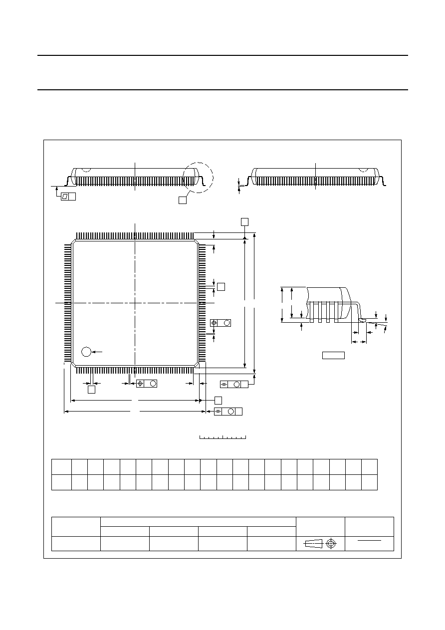
2004 Jan 26
66
Philips Semiconductors
Product specification
MPEG-2 video and MPEG-audio/AC-3
audio encoder with multiplexer
SAA6752HS
13 PACKAGE OUTLINE
UNIT
A
1
A
2
A
3
b
p
c
E
(1)
e
H
E
L
L
p
Z
y
w
v
REFERENCES
OUTLINE
VERSION
EUROPEAN
PROJECTION
ISSUE DATE
IEC
JEDEC
JEITA
mm
0.50
0.25
3.6
3.2
0.25
0.27
0.17
0.20
0.09
28.1
27.9
0.5
30.9
30.3
1.39
1.11
8
0
o
o
0.08
0.2
1.3
0.08
DIMENSIONS (mm are the original dimensions)
Note
1. Plastic or metal protrusions of 0.25 mm maximum per side are not included.
0.75
0.45
SOT316-1
MS-029
00-01-25
03-02-25
D
(1)
(1)
(1)
28.1
27.9
H
D
30.9
30.3
E
Z
1.39
1.11
D
pin 1 index
b
p
e
E
A
1
A
L
p
detail X
L
(A )
3
B
52
c
D
H
b
p
E
H
A
2
v
M
B
D
Z D
A
Z E
e
v
M
A
X
1
208
157
156
105
104
53
y
w
M
w
M
0
5
10 mm
scale
208 leads (lead length 1.3 mm); body 28 x 28 x 3.4 mm; high stand-off height
SQFP208: plastic shrink quad flat package;
SOT316-1
A
max.
4.1

2004 Jan 26
67
Philips Semiconductors
Product specification
MPEG-2 video and MPEG-audio/AC-3
audio encoder with multiplexer
SAA6752HS
14 SOLDERING
14.1
Introduction to soldering surface mount
packages
This text gives a very brief insight to a complex technology.
A more in-depth account of soldering ICs can be found in
our
"Data Handbook IC26; Integrated Circuit Packages"
(document order number 9398 652 90011).
There is no soldering method that is ideal for all surface
mount IC packages. Wave soldering can still be used for
certain surface mount ICs, but it is not suitable for fine pitch
SMDs. In these situations reflow soldering is
recommended.
14.2
Reflow soldering
Reflow soldering requires solder paste (a suspension of
fine solder particles, flux and binding agent) to be applied
to the printed-circuit board by screen printing, stencilling or
pressure-syringe dispensing before package placement.
Driven by legislation and environmental forces the
worldwide use of lead-free solder pastes is increasing.
Several methods exist for reflowing; for example,
convection or convection/infrared heating in a conveyor
type oven. Throughput times (preheating, soldering and
cooling) vary between 100 and 200 seconds depending
on heating method.
Typical reflow peak temperatures range from
215 to 270
∞
C depending on solder paste material. The
top-surface temperature of the packages should
preferably be kept:
∑
below 225
∞
C (SnPb process) or below 245
∞
C (Pb-free
process)
≠ for all BGA, HTSSON-T and SSOP-T packages
≠ for packages with a thickness
2.5 mm
≠ for packages with a thickness < 2.5 mm and a
volume
350 mm
3
so called thick/large packages.
∑
below 240
∞
C (SnPb process) or below 260
∞
C (Pb-free
process) for packages with a thickness < 2.5 mm and a
volume < 350 mm
3
so called small/thin packages.
Moisture sensitivity precautions, as indicated on packing,
must be respected at all times.
14.3
Wave soldering
Conventional single wave soldering is not recommended
for surface mount devices (SMDs) or printed-circuit boards
with a high component density, as solder bridging and
non-wetting can present major problems.
To overcome these problems the double-wave soldering
method was specifically developed.
If wave soldering is used the following conditions must be
observed for optimal results:
∑
Use a double-wave soldering method comprising a
turbulent wave with high upward pressure followed by a
smooth laminar wave.
∑
For packages with leads on two sides and a pitch (e):
≠ larger than or equal to 1.27 mm, the footprint
longitudinal axis is preferred to be parallel to the
transport direction of the printed-circuit board;
≠ smaller than 1.27 mm, the footprint longitudinal axis
must be parallel to the transport direction of the
printed-circuit board.
The footprint must incorporate solder thieves at the
downstream end.
∑
For packages with leads on four sides, the footprint must
be placed at a 45
∞
angle to the transport direction of the
printed-circuit board. The footprint must incorporate
solder thieves downstream and at the side corners.
During placement and before soldering, the package must
be fixed with a droplet of adhesive. The adhesive can be
applied by screen printing, pin transfer or syringe
dispensing. The package can be soldered after the
adhesive is cured.
Typical dwell time of the leads in the wave ranges from
3 to 4 seconds at 250
∞
C or 265
∞
C, depending on solder
material applied, SnPb or Pb-free respectively.
A mildly-activated flux will eliminate the need for removal
of corrosive residues in most applications.
14.4
Manual soldering
Fix the component by first soldering two
diagonally-opposite end leads. Use a low voltage (24 V or
less) soldering iron applied to the flat part of the lead.
Contact time must be limited to 10 seconds at up to
300
∞
C.
When using a dedicated tool, all other leads can be
soldered in one operation within 2 to 5 seconds between
270 and 320
∞
C.

2004 Jan 26
68
Philips Semiconductors
Product specification
MPEG-2 video and MPEG-audio/AC-3
audio encoder with multiplexer
SAA6752HS
14.5
Suitability of surface mount IC packages for wave and reflow soldering methods
Notes
1. For more detailed information on the BGA packages refer to the
"(LF)BGA Application Note" (AN01026); order a copy
from your Philips Semiconductors sales office.
2. All surface mount (SMD) packages are moisture sensitive. Depending upon the moisture content, the maximum
temperature (with respect to time) and body size of the package, there is a risk that internal or external package
cracks may occur due to vaporization of the moisture in them (the so called popcorn effect). For details, refer to the
Drypack information in the
"Data Handbook IC26; Integrated Circuit Packages; Section: Packing Methods".
3. These transparent plastic packages are extremely sensitive to reflow soldering conditions and must on no account
be processed through more than one soldering cycle or subjected to infrared reflow soldering with peak temperature
exceeding 217
∞
C
±
10
∞
C measured in the atmosphere of the reflow oven. The package body peak temperature
must be kept as low as possible.
4. These packages are not suitable for wave soldering. On versions with the heatsink on the bottom side, the solder
cannot penetrate between the printed-circuit board and the heatsink. On versions with the heatsink on the top side,
the solder might be deposited on the heatsink surface.
5. If wave soldering is considered, then the package must be placed at a 45
∞
angle to the solder wave direction.
The package footprint must incorporate solder thieves downstream and at the side corners.
6. Wave soldering is suitable for LQFP, TQFP and QFP packages with a pitch (e) larger than 0.8 mm; it is definitely not
suitable for packages with a pitch (e) equal to or smaller than 0.65 mm.
7. Wave soldering is suitable for SSOP, TSSOP, VSO and VSSOP packages with a pitch (e) equal to or larger than
0.65 mm; it is definitely not suitable for packages with a pitch (e) equal to or smaller than 0.5 mm.
8. Image sensor packages in principle should not be soldered. They are mounted in sockets or delivered pre-mounted
on flex foil. However, the image sensor package can be mounted by the client on a flex foil by using a hot bar
soldering process. The appropriate soldering profile can be provided on request.
9. Hot bar or manual soldering is suitable for PMFP packages.
PACKAGE
(1)
SOLDERING METHOD
WAVE
REFLOW
(2)
BGA, HTSSON..T
(3)
, LBGA, LFBGA, SQFP, SSOP..T
(3)
, TFBGA,
USON, VFBGA
not suitable
suitable
DHVQFN, HBCC, HBGA, HLQFP, HSO, HSOP, HSQFP, HSSON,
HTQFP, HTSSOP, HVQFN, HVSON, SMS
not suitable
(4)
suitable
PLCC
(5)
, SO, SOJ
suitable
suitable
LQFP, QFP, TQFP
not recommended
(5)(6)
suitable
SSOP, TSSOP, VSO, VSSOP
not recommended
(7)
suitable
CWQCCN..L
(8)
, PMFP
(9)
, WQCCN..L
(8)
not suitable
not suitable

2004 Jan 26
69
Philips Semiconductors
Product specification
MPEG-2 video and MPEG-audio/AC-3
audio encoder with multiplexer
SAA6752HS
15 DATA SHEET STATUS
Notes
1. Please consult the most recently issued data sheet before initiating or completing a design.
2. The product status of the device(s) described in this data sheet may have changed since this data sheet was
published. The latest information is available on the Internet at URL http://www.semiconductors.philips.com.
3. For data sheets describing multiple type numbers, the highest-level product status determines the data sheet status.
LEVEL
DATA SHEET
STATUS
(1)
PRODUCT
STATUS
(2)(3)
DEFINITION
I
Objective data
Development
This data sheet contains data from the objective specification for product
development. Philips Semiconductors reserves the right to change the
specification in any manner without notice.
II
Preliminary data Qualification
This data sheet contains data from the preliminary specification.
Supplementary data will be published at a later date. Philips
Semiconductors reserves the right to change the specification without
notice, in order to improve the design and supply the best possible
product.
III
Product data
Production
This data sheet contains data from the product specification. Philips
Semiconductors reserves the right to make changes at any time in order
to improve the design, manufacturing and supply. Relevant changes will
be communicated via a Customer Product/Process Change Notification
(CPCN).
16 DEFINITIONS
Short-form specification
The data in a short-form
specification is extracted from a full data sheet with the
same type number and title. For detailed information see
the relevant data sheet or data handbook.
Limiting values definition
Limiting values given are in
accordance with the Absolute Maximum Rating System
(IEC 60134). Stress above one or more of the limiting
values may cause permanent damage to the device.
These are stress ratings only and operation of the device
at these or at any other conditions above those given in the
Characteristics sections of the specification is not implied.
Exposure to limiting values for extended periods may
affect device reliability.
Application information
Applications that are
described herein for any of these products are for
illustrative purposes only. Philips Semiconductors make
no representation or warranty that such applications will be
suitable for the specified use without further testing or
modification.
17 DISCLAIMERS
Life support applications
These products are not
designed for use in life support appliances, devices, or
systems where malfunction of these products can
reasonably be expected to result in personal injury. Philips
Semiconductors customers using or selling these products
for use in such applications do so at their own risk and
agree to fully indemnify Philips Semiconductors for any
damages resulting from such application.
Right to make changes
Philips Semiconductors
reserves the right to make changes in the products -
including circuits, standard cells, and/or software -
described or contained herein in order to improve design
and/or performance. When the product is in full production
(status `Production'), relevant changes will be
communicated via a Customer Product/Process Change
Notification (CPCN). Philips Semiconductors assumes no
responsibility or liability for the use of any of these
products, conveys no licence or title under any patent,
copyright, or mask work right to these products, and
makes no representations or warranties that these
products are free from patent, copyright, or mask work
right infringement, unless otherwise specified.

2004 Jan 26
70
Philips Semiconductors
Product specification
MPEG-2 video and MPEG-audio/AC-3
audio encoder with multiplexer
SAA6752HS
ICs with MPEG-audio/AC-3 audio functionality
Purchase of a Philips IC with an MPEG-audio and/or AC-3
audio functionality does not convey an implied license
under any patent right to use this IC in any MPEG-audio or
AC-3 audio application. A license can be obtained via
Philips Intellectual Property & Standards
(Internet at URL http://www.ip.philips.com;
e-mail info.licensing@philips.com).
ICs with MPEG-2 functionality
Use of this product in
any manner that complies with the MPEG-2 Standard is
expressly prohibited without a license under applicable
patents in the MPEG-2 patent portfolio, which license is
available from MPEG LA, L.L.C., 250 Steele Street, Suite
300, Denver, Colorado 80206.
18 PURCHASE OF PHILIPS I
2
C COMPONENTS
Purchase of Philips I
2
C components conveys a license under the Philips' I
2
C patent to use the
components in the I
2
C system provided the system conforms to the I
2
C specification defined by
Philips. This specification can be ordered using the code 9398 393 40011.

© Koninklijke Philips Electronics N.V. 2004
SCA76
All rights are reserved. Reproduction in whole or in part is prohibited without the prior written consent of the copyright owner.
The information presented in this document does not form part of any quotation or contract, is believed to be accurate and reliable and may be changed
without notice. No liability will be accepted by the publisher for any consequence of its use. Publication thereof does not convey nor imply any license
under patent- or other industrial or intellectual property rights.
Philips Semiconductors ≠ a worldwide company
Contact information
For additional information please visit http://www.semiconductors.philips.com.
Fax: +31 40 27 24825
For sales offices addresses send e-mail to: sales.addresses@www.semiconductors.philips.com.
Printed in The Netherlands
R04/03/pp
71
Date of release:
2004 Jan 26
Document order number:
9397 750 12538