 | –≠–ª–µ–∫—Ç—Ä–æ–Ω–Ω—ã–π –∫–æ–º–ø–æ–Ω–µ–Ω—Ç: TDA5341 | –°–∫–∞—á–∞—Ç—å:  PDF PDF  ZIP ZIP |

DATA SHEET
Product specification
File under Integrated Circuits, IC11
1997 Jul 10
INTEGRATED CIRCUITS
TDA5341
Brushless DC motor and VCM drive
circuit with speed control

1997 Jul 10
2
Philips Semiconductors
Product specification
Brushless DC motor and VCM drive circuit
with speed control
TDA5341
FEATURES
∑
Full-wave commutation (using push-pull output stages)
without position sensors
∑
Built-in start-up circuitry
∑
Three push-pull MOS outputs:
≠ 1 A output current
≠ Low voltage drop
≠ Built-in current limiter
∑
Thermal protection
∑
General purpose operational amplifier
∑
Reset generator
∑
Motor brake facility
∑
Actuator driver (H-bridge current-controlled)
∑
Power-down detector
∑
Automatic park and brake procedure
∑
Adjustable park voltage
∑
Sleep mode
∑
Speed control with Frequency-Locked Loop (FLL)
∑
Serial port
∑
Friction reduction prior to spin-up.
APPLICATIONS
∑
Hard Disk Drive (HDD).
GENERAL DESCRIPTION
The TDA5341 is a BiCMOS integrated circuit used to drive
brushless DC motors in full-wave mode. The device
senses the rotor position using an EMF sensing technique
and is ideally suited as a drive circuit for a hard disk drive
motor.
The TDA5341 also includes a Voice Coil Motor driver
(VCM), reset and park facilities and an accurate speed
regulator. In addition, a serial port facilitates the control of
the device.
QUICK REFERENCE DATA
Measured over full voltage and temperature range.
ORDERING INFORMATION
SYMBOL
PARAMETER
MIN.
TYP.
MAX.
UNIT
V
DD
general supply voltage for logic and power
4.5
5.0
5.25
V
I
oMOT
motor output current
1.3
1.6
1.9
A
R
DS(MOT)
motor output resistance
-
1.1
1.56
I
oACT
actuator output current
0.7
1.1
1.4
A
R
DS(ACT)
actuator output resistance
-
2.0
2.5
TYPE
NUMBER
PACKAGE
NAME
DESCRIPTION
VERSION
TDA5341G
LQFP64
plastic low profile quad flat package; 64 leads; body 10
◊
10
◊
1.4 mm
SOT314-2
1997 Jul 10
3
Philips Semiconductors
Product specification
Brushless DC motor and VCM drive circuit
with speed control
TDA5341
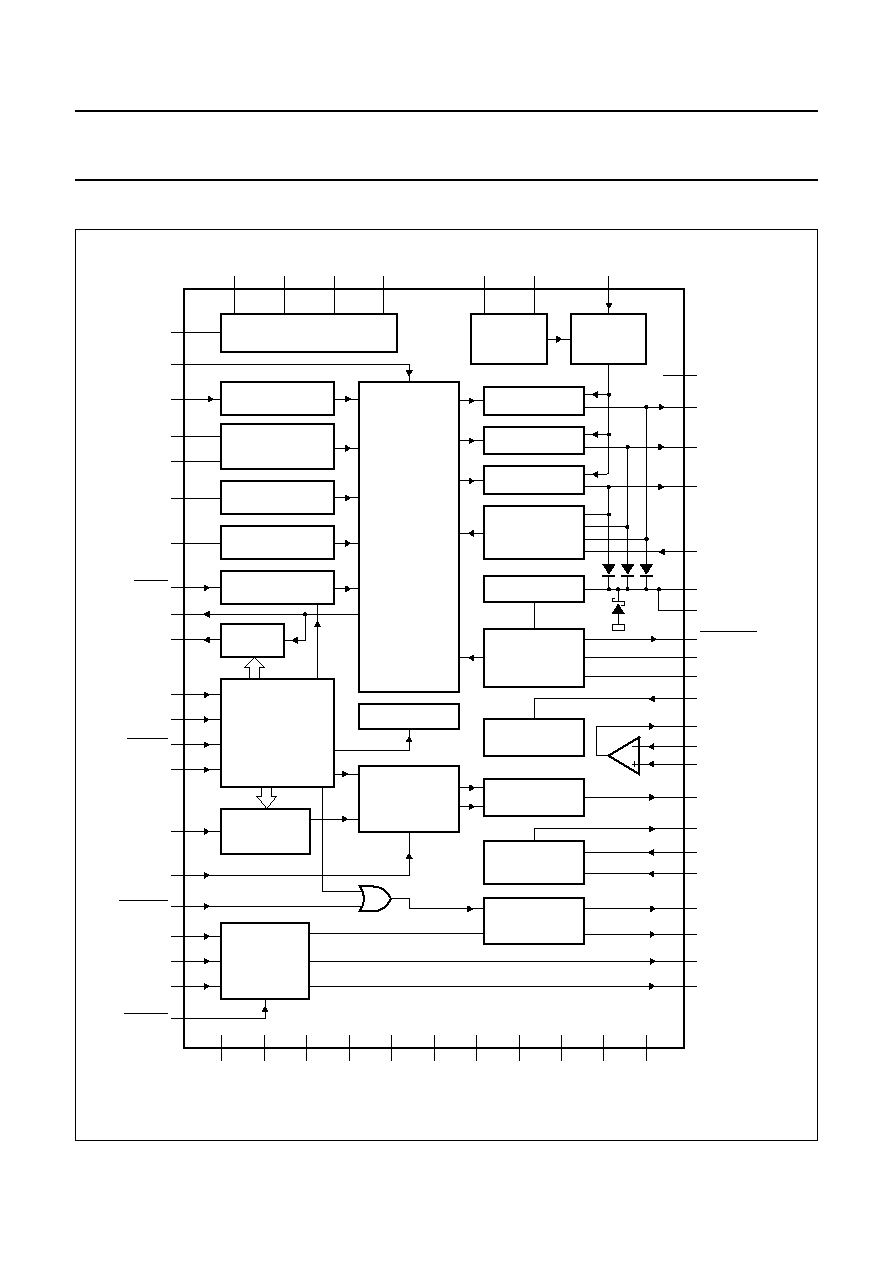
BLOCK DIAGRAM
Fig.1 Block diagram.
handbook, full pagewidth
MGE817
THERMAL
SWITCH
ADAPTIVE
COMMUTATION
DELAY
TIMING
OSCILLATOR
START
OSCILLATOR
BRAKE
CONTROLLER
COMMUTATION
AND
OUTPUT
DRIVING
LOGIC
POWER 1
POWER 2
POWER 3
COMPARATORS
BAND GAP 2
BAND GAP 1
UNDER-VOLTAGE
DETECTOR
POLES
DIVIDER
SERIAL
PORT
PROGRAMMING
FREQUENCY
DIVIDER
DIGITAL
FREQUENCY
COMPARATOR
BRAKE
AFTER PARK
CHARGE
PUMP
SENSE
AMPLIFIER
VCM
H-BRIDGE
VCM
PREAMPLIFIER
CURRENT
LIMIT
CONTROL
CONTROL
AMPLIFIER
UPPER VOLTAGE
CONVERTER
50
14
55
31
49
17
TDA5341
25
64
40
16
41
29
28
45
37
51
52
53
32
6
5
4
46
54
43
44
26
3
7
21
8
60
20
23
22
24
63
62
59
61
27
9
12
18
19
2
1
11
10
58
39
38
42
57
48
35
30
park
fill
sleep
brake
33
34
36
15
PRESET
MOT1
MOT2
MOT3
MOT0
CLAMP1
CLAMP2
UVDIN1
UVDIN2
BRAKEDELAY
AMPOUT
AMPIN
-
AMPIN
+
FILTER
SENSEOUT
SENSEIN
+
SENSEIN
-
VCM
+
VCM
-
FB1
FB2
RESETOUT
CAPXA
CAPXB
CAPYA
CAPYB
CNTRL
CAPCPC
ILIM
CAPCP
FREDENA
TESTIN
CAPCDM
CAPCDS
CAPTI
CAPST
FG
FMOT
CLOCK
DATA
ENABLE
RESET
ROSC
DPULSE
RETRACT
VCMIN1
VCMIN2
Vref
GAINSEL
BRAKE
VEED
VEE1
VEE2
VEE3
VEE4
VEE
VDD1
VDD2
VDD3
VDD
VDDD

1997 Jul 10
4
Philips Semiconductors
Product specification
Brushless DC motor and VCM drive circuit
with speed control
TDA5341
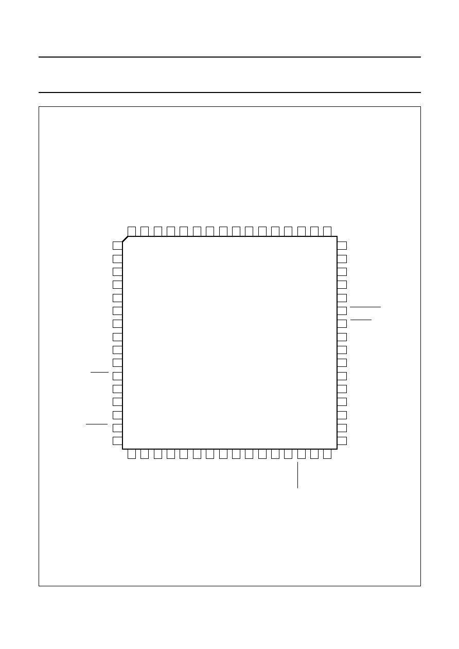
PINNING
SYMBOL
PIN
DESCRIPTION
CAPST
1
external capacitor for starting oscillator
CAPTI
2
external capacitor for timer circuit
CLAMP1
3
external capacitor used to park the heads; must be externally connected to CLAMP2
AMPOUT
4
uncommitted operational amplifier output
AMPIN
-
5
uncommitted operational amplifier invert input
AMPIN+
6
uncommitted operational amplifier direct input
MOT0
7
motor centre tap input
MOT2
8
motor driver output 2
FREDENA
9
friction reduction mode enable input (active HIGH)
FG
10
frequency generator (tacho) output
BRAKE
11
brake input command (active LOW)
TESTIN
12
test input for power output switch-off (active HIGH)
TP1
13
test purpose 1 (should be left open-circuit)
V
EE1
14
ground for the spindle motor drivers
GAINSEL
15
VCM gain adjustment input (switch ON when GAINSEL is LOW)
V
DD
16
general power supply
V
EE
17
general ground
CAPCDM
18
external capacitor for adaptive commutation delay (master)
CAPCDS
19
external capacitor for adaptive commutation delay (slave)
PRESET
20
set the motor drivers into a fixed state: MOT1 = F (floating), MOT2 = L, MOT3 = H
MOT3
21
motor driver output 3
CAPCPC
22
frequency compensation of the current control
ILIM
23
current limit control input
CNTRL
24
motor control
V
DD1
25
power supply 1 for the spindle motor drivers
CLAMP2
26
external capacitor used to park the heads; must be externally connected to CLAMP1
CAPCP
27
external capacitor for the charge pump output
FB1
28
output of the VCM preamplifiers
FB2
29
switchable output of the VCM preamplifier
RETRACT
30
park input command (active LOW)
V
EE3
31
ground 3 for the actuator driver
FILTER
32
charge pump output to be connected to an external filter
V
CMIN1
33
VCM voltage control input
V
CMIN2
34
switchable VCM voltage control input
DPULSE
35
data pulse input of the frequency comparator of the speed control
V
ref
36
voltage reference input
VCM+
37
positive output of the VCM amplifier
DATA
38
input data of the serial port (active HIGH)
CLOCK
39
clock input signal to shift DATA into SERIALIN register (active HIGH)
V
DD3
40
power supply 3 for the actuator driver

1997 Jul 10
5
Philips Semiconductors
Product specification
Brushless DC motor and VCM drive circuit
with speed control
TDA5341
V
DDD
41
digital power supply
ENABLE
42
enable input; enables the serial port, i.e. allows DATA to be shifted in (active LOW)
RESETOUT
43
under-voltage detector output flag (active LOW)
UVDIN1
44
external capacitor for the RESETOUT duration
VCM
-
45
negative output of the VCM amplifier
BRAKEDELAY
46
delay control input for brake after park
TP2
47
test purpose 2 (should be left open-circuit)
ROSC
48
reference oscillator input for motor speed control
V
EE4
49
ground 4 for the actuator driver
V
EED
50
digital ground
SENSEIN
-
51
inverting input of the VCM sense amplifier
SENSEN+
52
non-inverting input of the VCM sense amplifier
SENSEOUT
53
output of the VCM sense amplifier
UVDIN2
54
external voltage reference for the under-voltage detector
V
EE2
55
ground 2 for the spindle motor drivers
TP3
56
test purpose 3 (should be left open-circuit)
RESET
57
reset input; forces all bits of the SERIALIN register to 0 (active HIGH)
FMOT
58
tachometer output (one pulse per mechanical revolution)
CAPXB
59
external capacitor for the charge pump output
MOT1
60
motor driver output 1
CAPXA
61
external capacitor for the charge pump output
CAPYA
62
external capacitor for the charge pump output
CAPYB
63
external capacitor for the charge pump output
V
DD2
64
power supply for the spindle motor drivers
SYMBOL
PIN
DESCRIPTION
1997 Jul 10
6
Philips Semiconductors
Product specification
Brushless DC motor and VCM drive circuit
with speed control
TDA5341
Fig.2 Pinning diagram.
handbook, full pagewidth
TDA5341
MGE816
1
2
3
4
5
6
7
8
9
10
11
12
13
14
15
16
48
47
46
45
44
43
42
41
40
39
38
37
36
35
34
33
ROSC
TP2
BRAKEDELAY
VCM
-
UVDIN1
RESETOUT
ENABLE
VDDD
VDD3
CLOCK
DATA
VCM
+
Vref
DPULSE
VCMIN2
VCMIN1
CAPST
CAPTI
CLAMP1
AMPOUT
AMPIN
-
AMPIN
+
MOT0
MOT2
FREDENA
FG
BRAKE
TESTIN
TP1
VEE1
GAINSEL
VDD
17
18
19
20
21
22
23
24
25
26
27
28
29
30
31
32
64
63
62
61
60
59
58
57
56
55
54
53
52
51
50
49
V
DD2
CAPYB
CAPYA
CAPXA
MOT1
CAPXB
FMOT
RESET
TP3
V
EE2
UVDIN2
SENSEOUT
SENSEIN
+
SENSEIN
-
V
EED
V
EE4
V
EE
CAPCDM
CAPCDS
PRESET
MOT3
CAPCPC
ILIM
CNTRL
V
DD1
CLAMP2
CAPCP
FB1
FB2
RETRACT
V
EE3
FILTER

1997 Jul 10
7
Philips Semiconductors
Product specification
Brushless DC motor and VCM drive circuit
with speed control
TDA5341
FUNCTIONAL DESCRIPTION
The TDA5341 offers a sensorless three-phase motor
full-wave drive function. The device also offers protected
outputs capable of handling high currents and can be used
with star or delta connected motors.
The TDA5341 can easily be adapted for different motors
and applications.
The TDA5341 offers the following features:
∑
Sensorless commutation by using the motor EMF
∑
Built-in start-up circuit
∑
Optimum commutation, independent of motor type or
motor loading
∑
Built-in flyback diodes
∑
Three-phase full-wave drive
∑
High output current (1.3 A)
∑
Low MOS R
DSon
(1
)
∑
Outputs protected by current limitation and thermal
protection of each output transistor
∑
Low current consumption
∑
Additional uncommitted operational amplifier
∑
H-bridge actuator driver current controlled with an
external series sense resistor
∑
Automatic retract procedure
∑
Adjustable park voltage
∑
Sleep mode
∑
Automatic brake (after park) procedure
∑
Speed control based on FLL technique
∑
Serial port DATAIN (24 bits)
∑
Friction reduction prior to spin-up.
TDA5341 modes description
The TDA5341 can be used in two main modes, depending
on whether they are controlled or not.
The `controlled modes' (user commands) are executed by
the TDA5341 without delay or priority treatment, either by
software via the serial port or by hardware. BRAKE is a
hardware command whereas RETRACT can be controlled
in both ways. If it is preferable to control the heads parking
via the serial bus, the equivalent pin can be left
open-circuit.
The sleep mode is controlled by software only; it results
from the combination of the spindle and actuator being
disabled. The spindle is turned off by bit SPINDLE
DISABLE, whereas the actuator is disabled towards bit
VCM DISABLE of the serial port (see Section "Serial
port"). In addition, a special spin-up mode can be activated
in the event of high head stiction
The `uncontrolled modes' only result from different failures
caused by either a too high internal temperature or an
abnormally low power voltage, which will cause the
actuator to retract and, after the spindle, to brake.
The output signals mainly affected by those failures are
RESETOUT, MOT1, 2 and 3, VCM+ and VCM
-
. This is
summarised in Tables 1 and 2.
Table 1
Summary of controlled modes
HARDWARE/
SOFTWARE
MODE
MOT1, 2 AND 3
VCM+ AND
VCM
-
RESETOUT
EFFECT
Software
spindle disable
high impedance
high impedance
HIGH
spindle off
Software
VCM disable
not affected
high impedance
HIGH
spindle on; VCM off
Hardware
brake
LOW
not affected
HIGH
spindle coils ground
Software/
hardware
retract
not affected
VCM
-
= 0.65 V;
VCM+ = 0 V
HIGH
heads parked
Hardware
friction reduction
-
not affected
HIGH
heads in vibration

1997 Jul 10
8
Philips Semiconductors
Product specification
Brushless DC motor and VCM drive circuit
with speed control
TDA5341
Table 2
Summary of uncontrolled modes
FAILURE
MOT1, 2 AND 3
VCM+ AND VCM
-
RESETOUT
EFFECT
Thermal
shut-down
high impedance
LOW
VCM
-
= 0.65 V;
VCM+ = 0 V
LOW
automatic park and brake
Voltage
shut-down
high impedance
LOW
VCM
-
= 0.65 V;
VCM+ = 0 V
LOW
automatic park and brake
Controlled modes
S
PINDLE DISABLE
The spindle circuitry is switched off when bit 23 (SPINDLE
DISABLE) of the serial port is pulled HIGH. In that mode,
the reference band gap generator is cut off so that all
internal current sources are disabled. Both the spindle and
actuator outputs will be set to the high impedance state
because the upper converter is also turned off.
It should be noted that the uncommitted operational
amplifier is also disabled in that mode.
VCM
DISABLE
The actuator will be disabled when bit 22 (VCM DISABLE)
is set to logic 1; the spindle circuitry is not affected in that
mode. The retract circuitry also remains active, so that the
heads can be parked although the VCM is disabled. In that
mode, the current consumption can be reduced by
±
4 mA.
S
LEEP MODE
The sleep mode is obtained by pulling both the SPINDLE
and VCM DISABLE bits of the serial port HIGH. The power
monitor circuitry only remains active in sleep mode.
R
ETRACT
Retract is activated by pulling either bit 21 (PARK) HIGH
or RETRACT (pin 30) LOW. When RETRACT is set LOW,
a voltage of 0.65 V is applied to pin VCM
-
for parking.
It should be noted that the park voltage can be made
adjustable by changing one of the interconnect masks.
Accordingly, some different voltages, varying from
0.2 to 1.2 V, can quickly be obtained on customer
demand. This mode does not affect the control of the
spindle rotation.
B
RAKE MODE
The brake mode is activated by pulling BRAKE (pin 11)
LOW. When a voltage of less than 0.8 V is applied to pin
BRAKE, the 3 motor outputs are short-circuited to ground,
which results in a quick reduction of the speed until the
motor stops completely.
F
RICTION REDUCTION
Pulling FREDENA HIGH activates the friction reduction
mode of the TDA5341. In that mode, a clock signal fed via
pin TESTIN will cause the MOT outputs to sequentially
switch-on and switch-off at the same frequency and, as a
result, generate an AC spindle torque high enough to
overcome the head stiction.
Before start-up, the head stiction might be higher than
normal due to condensation between the head(s) and the
disk(s). Normal spin-up is not possible when this friction
torque is higher than the start-up torque of the spindle
motor. Spin-up is then only possible after friction has been
reduced by breaking the head(s) free. Bringing a static
friction system into mechanical resonance is an effective
method to break static friction head(s) free.
The resonance frequency is:
Where:
C = Stiffness of the head-spring(s) in direction of disk(s)
rotation, (N/m)
J = Inertia of the disk(s), (kg/m
2
).
The external clock input frequency must be:
A burst of n
◊
6 clock pulse will bring the system into
resonance and break the heads free (n > 2). Once the
heads have been broken free, the normal spin-up
procedure can be applied.
It should be noted that the clock frequency must be smaller
than 40000/CAPCDM (nF).
f
res
1
2
-------
0.5
C
J
----
◊
=
f
clk
6
2
-------
0.5
C
J
----
◊
=

1997 Jul 10
9
Philips Semiconductors
Product specification
Brushless DC motor and VCM drive circuit
with speed control
TDA5341
Uncontrolled modes
P
OWER SHUT
-
DOWN
If the power supply decreases to less than the voltage
threshold determined by the ratio between R1 and R2
connected to UVDIN2 (see Fig.8) (for more than 1
µ
s), the
TDA5341 will issue a reset (RESETOUT goes LOW) and
the following operation will start:
∑
Firstly, the MOT outputs are switched to the high
impedance state so as to get back the rectified EMF
issued from the motor itself. At the same time, the
voltage upper converter is cut off in order to preserve the
voltage on the charge pump capacitance at CAPCP.
The energy supplied in that way is then used to park the
heads in a safe position
∑
Secondly, after a certain period of time, depending on
the RC constant of the device connected to
BRAKEDELAY, the lower MOS drivers will be turned on
in order to stop the motor completely.
T
HERMAL SHUT
-
DOWN
Should the temperature of the chip exceed +140
±
10
∞
C, a
shut-down operation will also be processed. The actions
described for power shut-down will be sequenced in the
same manner.
S
PINDLE SECTION
(see Fig.1)
Full-wave driving of a three-phase motor requires three
push-pull output stages. In each of the six possible states
two outputs are active, one sourcing current and one
sinking current. The third output presents a high
impedance to the motor which enables measurement of
the motor EMF in the corresponding motor coil by the EMF
comparator at each output. The commutation logic is
responsible for control of the output transistors and
selection of the correct EMF comparator.
The zero-crossing in the motor EMF (detected by the
comparator selected by the commutation logic) is used to
calculate the correct moment for the next commutation, i.e.
the change to the next output state. The delay is calculated
(depending on the motor loading) by the adaptive
commutation delay block.
Because of high inductive loading the output stages
contain flyback diodes. The output stages are also
protected by a current limiting circuit and by thermal
protection of the six output transistors.
The zero-crossings can be used to provide speed
information such as the tacho signal (FG).
The system will only function when the EMF voltage from
the motor is present. Consequently, a start oscillator is
provided that will generate commutation pulses when no
zero-crossings in the motor voltage are available.
A timing function is incorporated into the device for internal
timing and for timing of the reverse rotation detection.
The TDA5341 also contains a control amplifier, directly
driving output amplifiers.
The TDA5341 also provides access to the user of some of
its internal test modes. Firstly, a PRESET mode can be
used for prepositioning the three motor output drivers into
a fixed state. By pulling pin PRESET to 0.75 V above V
DD
,
MOT3 goes HIGH, MOT2 goes LOW and MOT1 goes to
the high impedance state.
In addition, when TESTIN is pulled HIGH (provided that
FREDENA is LOW), the 3 motor output drivers are
switched off. It should be noted that RESETOUT goes
LOW in that particular event.
Adjustments
The system has been designed in such a way that the
tolerances of the application components are not critical.
However, the approximate values of the following
components must still be determined:
∑
The start capacitor; this determines the frequency of the
start oscillator
∑
The two capacitors in the adaptive commutation delay
circuit; these are important in determining the optimum
moment for commutation, depending on the type and
loading of the motor
∑
The timing capacitor; this provides the system with its
timing signals.
The start capacitor (CAPST)
This capacitor determines the frequency of the start
oscillator. It is charged and discharged, with a current of
5.5
µ
A, from 0.05 to 2.2 V and back to 0.05 V. The time
taken to complete one cycle is given by:
t
start
= (0.78
◊
C); where C is given in
µ
F.
The start oscillator is reset by a commutation pulse and so
is only active when the system is in the start-up mode.
A pulse from the start oscillator will cause the outputs to
change to the next state (torque in the motor). If the
movement of the motor generates enough EMF the
TDA5341 will run the motor.

1997 Jul 10
10
Philips Semiconductors
Product specification
Brushless DC motor and VCM drive circuit
with speed control
TDA5341
If the amount of EMF generated is insufficient, then the
motor will move one step only and will oscillate in its new
position. The amplitude of the oscillation must decrease
sufficiently before the arrival of the next start pulse, to
prevent the pulse arriving during the wrong phase of the
oscillation. The oscillation of the motor is given by:
Where:
K
t
= torque constant (N.m/A)
I = current (A)
p = number of magnetic pole-pairs
J = inertia J (kg/m
2
).
Example: J = 6.34
◊
10
-
7
kg/m
2
, K = 4.5
◊
10
-
3
N.m/A,
p = 6 and I = 0.48 A; thus f
osc
= 22.7 Hz. Without
damping, a start frequency of 48.4 Hz can be chosen or
t = 24 ms, thus C = 0.024/0.78 = 0.031
µ
F, (choose
33 nF).
The Adaptive Commutation Delay
(CAPCDM and CAPCDS)
In this circuit capacitor CAPCDM is charged during one
commutation period, with an interruption of the charging
current during the diode pulse.
f
osc
0.5
--------
K
t
I
P
J
----
◊
◊
◊
1
2
---
=
During the next commutation period this capacitor
(CAPCDM) is discharged at twice the charging current.
The charging current is 10
µ
A and the discharging current
20
µ
A; the voltage range is from 0.87 to 2.28 V.
The voltage must stay within this range at the lowest
commutation frequency of interest, f
C1
:
Where C is in nF.
If the frequency is lower, then a constant commutation
delay after the zero-crossing is generated by the discharge
from 2.28 to 0.87 V at 20
µ
A.
Maximum delay = (0.070
◊
C) ms: Where C is in nF.
Example: nominal commutation frequency is 3240 Hz and
the lowest usable frequency is 1600 Hz, thus
CAPCDM = 7092/1600 = 4.43 (choose 4.7 nF)
The other capacitor, CAPCDS, is used to repeat the same
delay by charging and discharging with 20
µ
A. The same
value can be chosen as for CAPCDM. Figure 3 illustrates
typical voltage waveforms.
C
10
10
◊
6
≠
f
1.41
◊
------------------------
7092
f
C1
-------------
=
=
Fig.3 CAPCDM and CAPCDS voltage waveforms in normal running mode.
handbook, full pagewidth
MGE820
voltage
on CAPCDS
voltage
on CAPCDM

1997 Jul 10
11
Philips Semiconductors
Product specification
Brushless DC motor and VCM drive circuit
with speed control
TDA5341
The Timing Capacitor (CAPTI)
Capacitor CAPTI is used for timing the successive steps
within one commutation period; these steps include some
internal delays.
The most important function is the watchdog time in which
the motor EMF has to recover from a negative diode pulse
back to a positive EMF voltage (or vice-versa). A watchdog
timer is a guarding function that only becomes active when
the expected event does not occur within a predetermined
time.
The EMF usually recovers within a short time if the motor
is running normally (<<ms). However, if the motor is
motionless or rotating in the reverse direction, then the
time can be longer (>>ms).
A watchdog time must be chosen so that it is long enough
for a motor without EMF (still) and eddy currents that may
stretch the voltage in a motor winding. However, it must be
short enough to detect reverse rotation. If the watchdog
time is made too long, then the motor may run in the wrong
direction (with little torque).
The capacitor is charged, with a current of 60
µ
A, from
0.03 to 0.3 V. Above this level it is charged, with a current
of 5
µ
A, up to 2.2 V only if the selected motor EMF remains
in the wrong polarity (watchdog function). At the end, or, if
the motor voltage becomes positive, the capacitor is
discharged with a current of 30
µ
A. The watchdog time is
the time taken to charge the capacitor, with a current of
5
µ
A, from 0.3 to 2.2 V. The value of CAPTI is given by:
Where: C is in nF and t is in ms.
Example: If, after switching off, the voltage from a motor
winding is reduced, in 3.5 ms, to within 10 mV (the offset
of the EMF comparator), then the value of the required
timing capacitor is given by:
C = 2.63
◊
3.5 = 9.2 (choose 10 nF)
Typical voltage waveforms are illustrated by Fig.4.
C
5
10
6
≠
◊
t
m
1.9
--------
2.63t
m
=
◊
=
Fig.4 Typical CAPTI and V
MOT1
voltage waveforms in normal running mode.
If the chosen value of CAPTI is too small, then oscillations can occur in certain positions of a blocked rotor. If the chosen value is too large, then it is
possible that the motor may run in the reverse direction (synchronously with little torque).
handbook, full pagewidth
MGE821
voltage
on CAPTI
VMOT1
1997 Jul 10
12
Philips Semiconductors
Product specification
Brushless DC motor and VCM drive circuit
with speed control
TDA5341
Other design aspects
There are other design aspects concerning the application
of the TDA5341 besides the commutation function.
They are as follows:
∑
Generation of the tacho signal FG
∑
Motor control
∑
Current limiting
∑
Thermal protection.
FG signal
The FG signal is generated in the TDA5341 by using the
zero-crossing of the motor EMF from the three motor
windings and the commutation signal.
Output FG switches from HIGH-to-LOW on all
zero-crossings and LOW-to-HIGH on all commutations
and can source more than 40
µ
A and sink more than
1.6 mA.
Example: A three-phase motor with 6 magnetic pole-pairs
at 1500 rpm and with a full-wave drive has a commutation
frequency of 25
◊
6
◊
6 = 900 Hz and generates a tacho
signal of 900 Hz.
Motor control
Figure 5 shows the spindle transconductance by giving the
relative output current as a function of the voltage applied
to pin CNTRL.
handbook, halfpage
MGE822
0
5
100
0
20
40
60
80
1
2
3
4
control voltage (V)
Io
(% of Imax)
Fig.5 Output current control.
Current limiting
Outputs MOT1 to MOT3 are protected against high
currents in two ways; current limiting of the `lower' output
transistor and current limiting of the `upper' one.
This means that the current from and to the output stages
is limited.
It is possible to adjust the limiting current externally by
using an external resistor connected between pin ILIM and
ground, the value is determined by the formula:
Where R = R (min.) = 19.5 k
and I
ILIM
= 1.3 A.
If R < 19.5 k
, then I
ILIM
is internally limited for device
protection purposes.
Thermal protection
Thermal protection of the six output transistors of the
spindle section is achieved by each transistor having a
thermal sensor that is active when the transistor is
switched on. The transistors are switched off when the
local temperature becomes too high. In that event, a
RESET is automatically generated to the external world by
pulling RESETOUT LOW.
Reset section
This circuit provides the following:
∑
An external signal that sends a RESETOUT (active
LOW) to the disk drive circuitry at power-up and
power-down
∑
Causes actuator to retract (PARK).
The power-up reset signal (RESETOUT) applied to
external circuits as a digital output is typically 150 ms after
power-up. In the same way, as soon as V
DD
goes below a
threshold that is externally set (UVDIN2), RESETOUT
goes LOW. The under voltage detection threshold is
adjustable with external resistors (see Fig.8).
The reset circuitry has a minimum output pulse (100 ms)
even for brief power interruptions (higher than 1 ms).
The pulse duration can be adjusted with an external
capacitor (UVDIN1).
I
ILIM
10020
2.54
R
-----------
◊
=
1997 Jul 10
13
Philips Semiconductors
Product specification
Brushless DC motor and VCM drive circuit
with speed control
TDA5341
The power for retraction is received from the rectification
of the EMF of the spindle before it is spun down.
After retraction, a brake procedure is automatically settled.
The time needed for retraction, prior to braking, can be
precisely adjusted with the external RC device connected
to pin BRAKEDELAY. The discharge of the capacitance
across the resistance from V
DD
-
0.7 V down to 1 V will
provide the desired time constant.
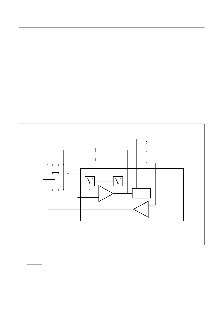
Actuator section
The actuator driver has a control input voltage that is
proportional to the actuator current which is capable of a
closed-loop band-pass frequency higher than 10 kHz.
An operational amplifier input allows passive external
components for compensation and gain setting.
The compensation amplifier is able to be pulled out of a
saturation state within 5
µ
s and its output swing is
V
DD
-
1.5 V.
An actuator current-sense amplifier is provided for use by
the disc drive controller. The gain from current-sense
resistor to sense the amplifier output is typically 10 (
±
3%)
and the output voltage swing is
±
1.25 V. An input common
mode range insures operation through all normal coil
voltage excursions. Maximum recovery time from
saturation is 20
µ
s (typ.).
T
RANSFER FUNCTION
With GAINSEL = HIGH; R
IN
= R
IN1
With GAINSEL = LOW;
Fig.6 VCM section application diagram.
handbook, full pagewidth
VCMIN2
RIN1
CL2
CL1
RIN2
Rf
VCMIN1
Vref
GAINSEL
input
FB2
FB1
actuator
VCM
-
SENSEIN
-
VCM
+
SENSEIN
+
SENSEOUT
PREAMP
SENSE
AMP
OUTPUT
GAIN 11
TDA5341
MGE825
Rs
T
11
R
f
◊
Z
L
◊
1
R
IN
R
f
R
s
R
f
Z
VCM
110
R
s
◊
Z
L
◊
+
◊
+
◊
(
)
◊
--------------------------------------------------------------------------------------------------------------------
◊
≠
=
R
IN
R
IN1
R
IN2
◊
R
IN1
R
IN2
+
------------------------------
=

1997 Jul 10
14
Philips Semiconductors
Product specification
Brushless DC motor and VCM drive circuit
with speed control
TDA5341
Speed control function
Speed control is efficiently achieved by the
frequency-locked loop circuitry which is enabled by bit D20
of the CONTROL register.
Its aim is to keep the tachometer signal set to a reference
programmed by the user via the serial port (see Section
"Serial port").
The FLL operates as follows:
When power is first applied to the circuit, the FILTER pin is
pulled HIGH so that maximum output current can be
sourced for optimum torque.
FG pulses will appear rapidly so as to provide a `clean'
clock signal (FMOT) that will issue one pulse per
mechanical revolution. This may be used for speed
regulation, by re-entering the signal through the DPULSE
pin. Then, after it has been synchronised to the ROSC
clock, it is compared to an accurate reference derived from
the ROSC clock and programmed by the user via the serial
port. The resulting variation in frequency generates a
speed error term that will switch a charge-pump up or
down in order to charge or discharge an external RC filter
(FILTER). The voltage at the FILTER pin is then used as
an input to the current control amplifier that regulates the
current in both upper and lower NMOS transistors.
A velocity regulation based upon (maximum) one
corrective action per mechanical revolution may be
considered insufficient in some applications. That is the
reason why the second input of the FLL circuitry was
intentionally left open-circuit and directly accessible to the
external world via pin DPULSE. In that way, total freedom
is given to the user to use any signal coming out of the
microcontroller in order to regulate the motor velocity with
a finer accuracy.
Moreover, a mixed regulation is also possible: firstly,
the FMOT signal is fed via DPULSE into the FLL circuitry
and then once data is read out off the disc, it is switched to
another clock signal with a higher frequency than FMOT.
Simultaneously, a new division factor is programmed via
the serial port.
It should be noted that there is no need for external
synchronization. However, it is recommended to change
the division factor and the DPULSE clock rate during the
period when FMOT is HIGH.
Serial port
The serial port operates as follows:
When ENABLE is HIGH, the serial port is disabled, which
means the TDA5341 functions regardless of any change
at pins DATA and CLOCK.
When ENABLE is set LOW some set-up time before the
falling edge of CLOCK, the serial port is enabled, i. e. data
is serially shifted into the 24-bit shift register on the falling
edge of the CLOCK signal. The least significant bit
(LSB = DATA 0) is the first in, DATA(23) the MSB is the
last in.
When ENABLE goes HIGH, the contents of the shift
register are loaded into the internal fixed register
(CONTROL register), it will not change until the next rising
edge of ENABLE.
It should be noted that when RESET goes HIGH it will
force all bits of the shift register and the control register to
logic 0. However, there is no reset effect on both power-up
and power-down i.e there is no correlation between
RESET and RESETOUT.
CLOCK can be stopped (either in the HIGH or LOW state)
once RESET or ENABLE have been asserted.
The 24-bit control register is organized as follows:
∑
D23: SPINDLE DISABLE
≠ When LOW, the spindle circuitry is enabled
∑
D22: VCM DISABLE
≠ When LOW, the actuator circuitry is enabled
∑
D21: PARK
≠ When HIGH, it enables the head retraction. This has
the same effect as pin RETRACT pulled LOW
∑
D20: FLL ENABLE
≠ When HIGH, it closes the complete speed regulation
loop
≠ When LOW, it will set the output of the charge pump
(FILTER) to the high impedance state
∑
D19 and D18
≠ The combination of these bits fixes the division factor
to apply on the FG signal with respect to the number
of poles.

1997 Jul 10
15
Philips Semiconductors
Product specification
Brushless DC motor and VCM drive circuit
with speed control
TDA5341
Table 3
Division factor
∑
D17 to D0
These bits program the division factor to apply to the
ROSC signal so as to generate a reference that will
precisely control the spindle rotation;
≠ The division factor can range from 8 (DIV = 1) to
8
◊
[2
18
-
1] = 2097144 (DIV = 3FFFF)
≠ The relationship between this division factor, ROSC
and the motor frequency is as follows:
DIVISION FACTOR = 7.5
◊
ROSC/MOTOR speed
where the MOTOR speed is given in rpm and ROSC
in Hz.
D19
D18
POLE PAIRS
0
0
4
0
1
6
1
0
8
1
1
12
Example: for a motor speed of 3600 rpm and a reference
oscillation ROSC of 16 MHz, the division factor that has to
be programmed via the bus, will be:
The resulting error will be less than 0.04 rpm.
DIV
7.5
16
10
6
≠
◊
3600
------------------------
◊
33333
=
=
LIMITING VALUES
In accordance with the Absolute Maximum Rating System (IEC 134).
HANDLING
Every pin withstands the ESD test in accordance with MIL-STD-883C. Method 3015 (HBM 1900
, 100 pF) 3 pulses
positive and 3 pulses negative on each pin with reference to ground. Class 1 : 0 to 1999 V.
THERMAL CHARACTERISTICS
SYMBOL
PARAMETER
MIN.
MAX.
UNIT
V
DD
positive supply voltage
-
5.5
V
V
i
input voltage (all pins)
-
0.3
V
DD
+ 0.3 V
V
60,8,21
output voltage pins MOT1, MOT2 and MOT3
-
0.25
+5.5
V
V
45,37,53
output voltage pins VCM
-
, VCM+ and SENSEOUT
0.7
V
DD
+ 0.7 V
V
1,2,18,19
input voltage pins CAPST, CAPTI, CAPCDM and CAPCDS
-
2.5
V
T
stg
IC storage temperature
-
55
+150
∞
C
T
amb
operating ambient temperature
0
+70
∞
C
P
tot
total power dissipation
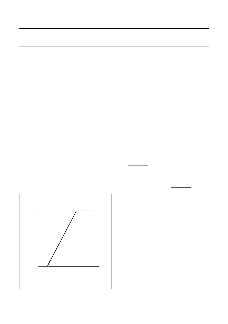
see Fig.7
SYMBOL
PARAMETER
VALUE
UNIT
R
th j-a
thermal resistance from junction to ambient in free air
54
K/W

1997 Jul 10
16
Philips Semiconductors
Product specification
Brushless DC motor and VCM drive circuit
with speed control
TDA5341
CHARACTERISTICS (SPINDLE FUNCTION)
V
DD
= 5 V; V
DD1
and V
DD2
> V
DD
is not allowed; T
amb
= 25
∞
C; unless otherwise specified.
SYMBOL
PARAMETER
CONDITIONS
MIN.
TYP.
MAX.
UNIT
Supply
V
DD
general supply voltage
4.5
5.0
5.25
V
V
DD1
supply voltage 1 for the spindle
motor drivers
4.5
5.0
5.25
V
V
DD2
supply voltage 2 for the spindle
motor drivers
4.5
5.0
5.25
V
V
DD3
supply voltage for the actuator
driver
4.5
5.0
5.25
V
I
DD
general supply current
-
11
15
mA
I
q(sm)
quiescent current in sleep mode
-
1.4
2
mA
Thermal protection
T
SD
local temperature at temperature
sensor causing shut-down
130
140
150
∞
C
T
reduction in temperature before
switch-on
after shut-down
-
T
SD
-
30
-
∞
C
V
so
test pin switch-off voltage
2.5
-
-
V
Fig.7 Power derating curve.
handbook, halfpage
0
50
150
Ptot
(W)
3
0
MGE823
100
Tamb (
∞
C)
1
2
(1)
(2)
SAFE
OPERATING
AREA
(1) T
j(max)
= 130
∞
C.
(2) T
j(max)
= 150
∞
C.

1997 Jul 10
17
Philips Semiconductors
Product specification
Brushless DC motor and VCM drive circuit
with speed control
TDA5341
MOT0
V
i
input voltage level
-
0.3
-
V
DD
-
1.7 V
I
bias
input bias current
-
1
-
0
µ
A
V
CSW
comparator switching voltage level
note 1
±
6.8
±
9.2
±
11.6
mV
V
CWS
variation in comparator switching
voltage levels within one IC
-
3.4
-
+3.4
mV
MOT1, MOT2 and MOT3; pins 60, 8 and 21
V
DO
drop-out voltage
I
o
= 250 mA
-
-
0.34
V
I
o
= 250 mA;
T
amb
= 70
∞
C
-
-
0.39
V
t
r
output rise time
from 0.2 to 0.8V
DD
10
25
35
µ
s
t
f
output fall time
from 0.8 to 0.2V
DD
10
25
35
µ
s
Output current limiting circuit; V
ILIM
= 5 V; pin 23
I
ILIM
limiting current (estimation)
R
ILIM
= 20 k
1.15
1.25
1.35
A
V
ILIM
input voltage
I
ILIM
= 100
µ
A
2.43
2.51
2.60
V
I
ILIM(CR)
limiting current control range
(estimation)
0.01
-
1.3
A
Output current control circuit; pin 24
V
CNTRL
input voltage level
0
-
V
DD
V
C
CPC
control loop stability capacitor
-
100
-
nF
CAPCPC; pin 22
I
o(sink)
output sink current
30
40
50
µ
A
I
o(source)
output source current
-
5.5
-
3.5
-
1.5
µ
A
CAPCP; pin 27
C
extCP
external output capacitor for the
charge pump
note 2
22
-
-
nF
I
o(sink)
output sink current
V
DD
= 0 V;
V
clamp
= 1.2 V
-
1
2.5
µ
A
V
CP
charge pump voltage
9.0
9.9
10.8
V
CAPST; pin 1
I
o(sink)
output sink current
4.5
6.0
7.5
µ
A
I
o(source)
output source current
-
7.0
-
5.5
-
4.0
µ
A
V
SW(L)
lower switching level
-
0.20
-
V
V
SW(M)
middle switching level
-
0.30
-
V
V
SW(H)
upper switching level
-
2.20
-
V
SYMBOL
PARAMETER
CONDITIONS
MIN.
TYP.
MAX.
UNIT
I
ILIM
I
o
10000
----------------
=

1997 Jul 10
18
Philips Semiconductors
Product specification
Brushless DC motor and VCM drive circuit
with speed control
TDA5341
Notes
1. Switching levels with respect to MOT1, MOT2 and MOT3.
2. CAPCP value is dependant of the powerless park and brake operations.
CAPTI; pin 2
I
o(sink)
output sink current
25
35
45
µ
A
I
oH(source)
HIGH level output source current
-
85
-
70
-
55
µ
A
I
oL(source)
LOW level lower source current
-
7.5
-
5.0
-
2.5
µ
A
V
SW(L)
lower switching level
-
30
-
mV
V
SW(M)
middle switching level
-
0.3
-
V
V
SW(H)
upper switching level
-
2.2
-
V
CAPCDM; pin 18
I
o(sink)
output sink current
13
20
27
µ
A
I
o(source)
output source current
-
13.5
-
10
-
6.5
µ
A
I
sink
/I
source
ratio of sink-to-source current
-
2.2
-
2.0
-
1.8
V
IL
LOW level input voltage
0.82
0.87
0.92
V
V
IH
HIGH level input voltage
2.20
2.28
2.37
V
CAPCDS; pin 19
I
o(sink)
output sink current
13
20
27
µ
A
I
o(source)
output source current
-
27
-
20
-
13
µ
A
I
sink
/I
source
ratio of sink-to-source current
-
1.1
-
1.0
-
0.9
µ
A
V
IL
LOW level input voltage
0.82
0.87
0.92
V
V
IH
HIGH level input voltage
2.20
2.28
2.37
V
FG; pin 10
V
OL
LOW level output voltage
I
o
= 0
µ
A
-
-
0.5
V
I
OL
LOW level output current
V
OL
= 1 V
3.3
5.3
-
mA
I
OH
HIGH level output current
V
OH
= 4.5 V
-
-
83
-
40
mA
R
F
ratio of FG frequency and
commutation frequency
-
1
-
duty factor
-
50
-
%
BRAKE; pin 11
I
NM
normal mode current
V
NM
= 2.8 V
-
40
-
27
-
µ
A
V
NM
normal mode voltage
2.65
-
V
DD
V
V
BM
brake mode voltage
-
-
2.35
V
I
BM
brake mode current
-
40
-
24
-
µ
A
Upper converter; pins 61 and 62
C
XA
external pump capacitor pin 61
-
10
-
nF
C
YA
external pump capacitor pin 62
-
10
-
nF
SYMBOL
PARAMETER
CONDITIONS
MIN.
TYP.
MAX.
UNIT

1997 Jul 10
19
Philips Semiconductors
Product specification
Brushless DC motor and VCM drive circuit
with speed control
TDA5341
CHARACTERISTICS (RESET FUNCTION)
V
DD
= 5 V; V
DD1
and V
DD2
> V
DD
is not allowed; T
amb
= 25
∞
C; unless otherwise specified.
SYMBOL
PARAMETER
CONDITIONS
MIN.
TYP.
MAX.
UNIT
UVDIN1; pin 44
I
UVDIN1
load capacitance current to
control the reset pulse width
-
2.3
-
1.7
-
1.3
µ
A
V
UVDIN1
input voltage threshold to
activate the reset output
2.4
2.55
2.75
V
UVDIN2; pin 54
V
UVDIN2
comparator voltage for
power-up and power-down
detection
see Fig.8
1.280
1.315
1.340
V
I
UVDIN2
input current
V
UVDIN2
= 1.6 V
-
0.5
-
+0.5
µ
A
RESETOUT; pin 43
V
PTH
power threshold voltage
see Fig.9
-
4.25
-
V
t
dPU
power-up reset delay
C = 0.1
µ
F;
see Fig.9
100
150
200
ms
t
dPD
power-down reset delay
see Fig.9
-
-
4
µ
s
t
PDW
power-down reset pulse width
see Fig.9
1.0
-
4
µ
s
t
W(min)
minimum output pulse width
C = 0.1
µ
F
100
-
-
ms
R
pu
pull-up resistance
6
10
14
k
V
OL
LOW level output voltage
I
OL
= 8.5 mA
-
-
0.5
V
Fig.8 Reset mode threshold.
handbook, halfpage
MGE818
VDD
R1
R2
UVDIN2
under-voltage threshold
1.32
R2
R1
+
(
)
R1
-----------------------------
◊
=
1997 Jul 10
20
Philips Semiconductors
Product specification
Brushless DC motor and VCM drive circuit
with speed control
TDA5341
CHARACTERISTICS (VCM FUNCTION)
V
DD
= 5 V; V
DD1
and V
DD2
> V
DD
is not allowed; T
amb
= 25
∞
C; unless otherwise specified.
SYMBOL
PARAMETER
CONDITIONS
MIN.
TYP.
MAX.
UNIT
SENSEIN
-
and SENSEIN+; pins 51 and 52
V
CS
common input sense voltage
0
-
V
DD
V
I
iSENSE
input sense current
-
250
-
+250
µ
A
SENSEOUT; pin 53
V
SENSE
differential output voltage
V
ref
= 1.9 to 2.6 V
0.5
V
ref
±
1.25
4.0
V
I
oSENSE
output sense current
-
250
-
+250
µ
A
G
SENSE
sense amplifier gain
9.9
10.2
10.5
f
co
cross-over frequency
-
40
-
MHz
V
o(os)
output offset voltage
I
SENSEIN
= 0
-
66
-
+66
mV
t
RSA
recovery time from saturation
-
20
-
µ
s
V
ref
; pin 36
V
ref
reference input voltage
1.9
-
2.6
V
I
ref
reference input current
-
5
-
+5
µ
A
Fig.9 Reset mode timing.
handbook, full pagewidth
MGE819
VDD
VPTH
VOH
VOL
VDD
RESETOUT
tdPU
tdPD
tW(min)
tPDW
>
4
µ
s
tPDW
<
1.2
µ
s
td

1997 Jul 10
21
Philips Semiconductors
Product specification
Brushless DC motor and VCM drive circuit
with speed control
TDA5341
VCM+ and VCM
-
; pins 37 and 45
V
CMdo
drop-out voltage
I
o
= 400 mA
-
0.8
1.0
V
I
oLIM
output current limiting
0.7
1.15
1.5
A
G
v
power amplifier voltage gain
9
-
12
V
oPARK
output park voltage
R
L
= 40
; note 1
-
0.75
-
V
VCMIN1 and VCMIN2
V
i
input voltage level
1.9
-
2.6
V
I
ibias
input bias current
-
-
0.25
µ
A
I
i(os)
input offset current
-
25
-
nA
GAINSEL; pin 15
V
IH
HIGH level input voltage
2
-
-
V
V
IL
LOW level input voltage
-
-
0.8
V
I
IH
HIGH level input current
-
10
-
+10
µ
A
I
IL
LOW level input current
-
20
-
+10
µ
A
R
SW
switch resistance
GAINSEL = LOW
-
-
40
GAINSEL = HIGH
10
-
-
M
FB1 and FB2; pins 28 and 29
V
i(os)
input offset voltage
-
5
-
+5
mV
V
FB
feed-back differential output
voltage
V
DD
= 5.25 V
±
0.4
-
±
V
DD
-
0.45
V
f
co
cross-over frequency
-
10
-
MHz
I
oFB
feed-back output current
-
250
+250
µ
A
t
RSB
recovery time from saturation
-
5
-
µ
s
R
SW
switch resistance
GAINSEL = LOW
-
-
40
GAINSEL = HIGH
10
-
-
M
RETRACT; pin 30
V
IH
HIGH level input voltage
2
-
-
V
V
IL
LOW level input voltage
-
-
0.8
V
I
IH
HIGH level input current
-
10
-
+10
µ
A
I
IL
LOW level input current
-
20
-
+10
µ
A
BRAKEDELAY; pin 46
V
BM
brake mode threshold voltage
-
0.75
1.0
V
V
NM
normal mode voltage
V
DD
-
0.85
-
-
V
SYMBOL
PARAMETER
CONDITIONS
MIN.
TYP.
MAX.
UNIT

1997 Jul 10
22
Philips Semiconductors
Product specification
Brushless DC motor and VCM drive circuit
with speed control
TDA5341
Note
1. This is the PARK default value. Other values can be obtained with a metal mask change.
CHARACTERISTICS (SPEED CONTROL FUNCTION)
V
DD
= 5 V; V
DD1
and V
DD2
> V
DD
is not allowed; T
amb
= 25
∞
C; unless otherwise specified.
Uncommitted operational amplifier; pins 4 to 6
V
i(os)
input offset voltage
-
3.5
-
+3.5
mV
I
i(bias)
input bias current
-
250
-
+250
nA
I
i(os)
input offset current
-
25
-
nA
V
CM
common mode voltage
1.7
-
2.6
V
G
OL
open loop gain
-
68
-
dB
f
co
cross-over frequency
-
10
-
MHz
V
OL
LOW level output voltage
I
OL
= 250
µ
A
-
-
0.7
V
V
OH
HIGH level output voltage
I
OH
=
-
250
µ
A
4.3
-
-
V
SYMBOL
PARAMETER
CONDITIONS
MIN.
TYP.
MAX.
UNIT
FILTER; pin 32
I
o(sink)
output sink current
80
100
120
µ
A
I
o(source)
output source current
-
110
-
90
-
70
µ
A
I
sink
/I
source
ratio of sink-to-source current
0.9
1.1
1.2
I
LO
charge pump leakage current
-
5
-
+5
nA
DATA, RESET and ENABLE; pins 38, 57 and 42
V
IL
LOW level input voltage
-
-
0.8
V
V
IH
HIGH level input voltage
2.4
-
-
V
I
i
input current
-
0
-
µ
A
CLOCK; pin 39
V
IL
LOW level input voltage
-
-
0.8
V
V
IH
HIGH level input voltage
2.4
-
-
V
f
clk
clock frequency
-
-
18
MHz
ROSC; pin 48
V
IL
LOW level input voltage
-
-
0.8
V
V
IH
HIGH level input voltage
2.4
-
-
V
f
refOSC
reference oscillator frequency
1
-
20
MHz
DPULSE; pin 35
V
IL
LOW level input voltage
-
-
0.8
V
V
IH
HIGH level input voltage
2.4
-
-
V
f
DPULSE
data pulse frequency
-
-
10
MHz
SYMBOL
PARAMETER
CONDITIONS
MIN.
TYP.
MAX.
UNIT
1997 Jul 10
23
Philips Semiconductors
Product specification
Brushless DC motor and VCM drive circuit
with speed control
TDA5341
FMOT; pin 58
V
OL
LOW level output voltage
I
OL
= 500
µ
A
-
-
0.1
V
duty factor
-
50
-
%
Timing; see Fig.10
t
su1
ENABLE set-up time
8
-
-
ns
t
su2
DATA set-up time
6
-
-
ns
t
h
DATA hold time
10
-
-
ns
SYMBOL
PARAMETER
CONDITIONS
MIN.
TYP.
MAX.
UNIT
Fig.10 Timing diagram.
handbook, full pagewidth
MGE824
SHIFTED
DATA
CLOCK
DATA
ENABLE
tsu1
tsu2
th
1997 Jul 10
24
Philips Semiconductors
Product specification
Brushless DC motor and VCM drive circuit
with speed control
TDA5341
APPLICATION INFORMATION
Fig.11 Application diagram of the TDA5341 in a hard disk drive.
handbook, full pagewidth
MGE826
MOT1
MOT2
MOT3
MOT0
CLAMP1 CLAMP2
RESETOUT
UVDIN1
UVDIN2
BRAKEDELAY
FILTER
SENSEOUT
SENSEIN
+
SENSEIN
-
VCM
+
VCM
-
FB1
FB2
CAPXA
CAPXB
CAPYA
CAPYB
CNTRL
CAPCPC
ILIM
CAPCP
FREDENA
TESTIN
CAPCDM
CAPCDS
CAPTI
CAPST
BRAKE
FMOT
CLOCK
DATA
ENABLE
RESET
ROSC
DPULSE
VCMIN1
VCMIN2
Vref
GAINSEL
RETRACT
VEED VEE1 VEE2 VEE3 VEE4 VEE
VDD1 VDD2 VDD3 VDD
VDDD
FG
+
5 V
+
5 V
SPINDLE
MOTOR
Rs
Rf
RIN1
RIN2
input
CL1
CL2
to micro-
controller
C2
C1
R1
24
32
9
39
38
42
57
48
12
43
11
10
58
35
27
61
59
62
63
18
19
2
1
50
14
55
31
49
17
36
46
29
34
28
33
53
52
51
37
45
15
30
54
44
22
23
7
21
8
60
26
3
41
16
40
64
25
TDA5341

1997 Jul 10
25
Philips Semiconductors
Product specification
Brushless DC motor and VCM drive circuit
with speed control
TDA5341
PACKAGE OUTLINE
UNIT
A
max.
A
1
A
2
A
3
b
p
c
E
(1)
e
H
E
L
L
p
Q
Z
y
w
v
REFERENCES
OUTLINE
VERSION
EUROPEAN
PROJECTION
ISSUE DATE
IEC
JEDEC
EIAJ
mm
1.60
0.20
0.05
1.45
1.35
0.25
0.27
0.17
0.18
0.12
10.1
9.9
0.5
12.15
11.85
0.69
0.59
1.45
1.05
7
0
o
o
0.12
0.1
1.0
0.2
DIMENSIONS (mm are the original dimensions)
Note
1. Plastic or metal protrusions of 0.25 mm maximum per side are not included.
0.75
0.45
SOT314-2
94-01-07
95-12-19
D
(1)
(1)
(1)
10.1
9.9
H
D
12.15
11.85
E
Z
1.45
1.05
D
b
p
e
E
A
1
A
L
p
Q
detail X
L
(A )
3
B
16
c
D
H
b
p
E
H
A
2
v
M
B
D
Z D
A
Z E
e
v
M
A
X
1
64
49
48
33
32
17
y
pin 1 index
w
M
w
M
0
2.5
5 mm
scale
LQFP64: plastic low profile quad flat package; 64 leads; body 10 x 10 x 1.4 mm
SOT314-2

1997 Jul 10
26
Philips Semiconductors
Product specification
Brushless DC motor and VCM drive circuit
with speed control
TDA5341
SOLDERING
Introduction
There is no soldering method that is ideal for all IC
packages. Wave soldering is often preferred when
through-hole and surface mounted components are mixed
on one printed-circuit board. However, wave soldering is
not always suitable for surface mounted ICs, or for
printed-circuits with high population densities. In these
situations reflow soldering is often used.
This text gives a very brief insight to a complex technology.
A more in-depth account of soldering ICs can be found in
our
"IC Package Databook" (order code 9398 652 90011).
Reflow soldering
Reflow soldering techniques are suitable for all LQFP
packages.
Reflow soldering requires solder paste (a suspension of
fine solder particles, flux and binding agent) to be applied
to the printed-circuit board by screen printing, stencilling or
pressure-syringe dispensing before package placement.
Several techniques exist for reflowing; for example,
thermal conduction by heated belt. Dwell times vary
between 50 and 300 seconds depending on heating
method. Typical reflow temperatures range from
215 to 250
∞
C.
Preheating is necessary to dry the paste and evaporate
the binding agent. Preheating duration: 45 minutes at
45
∞
C.
Wave soldering
Wave soldering is not recommended for LQFP packages.
This is because of the likelihood of solder bridging due to
closely-spaced leads and the possibility of incomplete
solder penetration in multi-lead devices.
If wave soldering cannot be avoided, the following
conditions must be observed:
∑
A double-wave (a turbulent wave with high upward
pressure followed by a smooth laminar wave)
soldering technique should be used.
∑
The footprint must be at an angle of 45
∞
to the board
direction and must incorporate solder thieves
downstream and at the side corners.
Even with these conditions, do not consider wave
soldering LQFP packages LQFP48 (SOT313-2),
LQFP64 (SOT314-2) or LQFP80 (SOT315-1).
During placement and before soldering, the package must
be fixed with a droplet of adhesive. The adhesive can be
applied by screen printing, pin transfer or syringe
dispensing. The package can be soldered after the
adhesive is cured.
Maximum permissible solder temperature is 260
∞
C, and
maximum duration of package immersion in solder is
10 seconds, if cooled to less than 150
∞
C within
6 seconds. Typical dwell time is 4 seconds at 250
∞
C.
A mildly-activated flux will eliminate the need for removal
of corrosive residues in most applications.
Repairing soldered joints
Fix the component by first soldering two diagonally-
opposite end leads. Use only a low voltage soldering iron
(less than 24 V) applied to the flat part of the lead. Contact
time must be limited to 10 seconds at up to 300
∞
C. When
using a dedicated tool, all other leads can be soldered in
one operation within 2 to 5 seconds between
270 and 320
∞
C.

1997 Jul 10
27
Philips Semiconductors
Product specification
Brushless DC motor and VCM drive circuit
with speed control
TDA5341
DEFINITIONS
LIFE SUPPORT APPLICATIONS
These products are not designed for use in life support appliances, devices, or systems where malfunction of these
products can reasonably be expected to result in personal injury. Philips customers using or selling these products for
use in such applications do so at their own risk and agree to fully indemnify Philips for any damages resulting from such
improper use or sale.
Data sheet status
Objective specification
This data sheet contains target or goal specifications for product development.
Preliminary specification
This data sheet contains preliminary data; supplementary data may be published later.
Product specification
This data sheet contains final product specifications.
Limiting values
Limiting values given are in accordance with the Absolute Maximum Rating System (IEC 134). Stress above one or
more of the limiting values may cause permanent damage to the device. These are stress ratings only and operation
of the device at these or at any other conditions above those given in the Characteristics sections of the specification
is not implied. Exposure to limiting values for extended periods may affect device reliability.
Application information
Where application information is given, it is advisory and does not form part of the specification.

Internet: http://www.semiconductors.philips.com
Philips Semiconductors ≠ a worldwide company
© Philips Electronics N.V. 1997
SCA55
All rights are reserved. Reproduction in whole or in part is prohibited without the prior written consent of the copyright owner.
The information presented in this document does not form part of any quotation or contract, is believed to be accurate and reliable and may be changed
without notice. No liability will be accepted by the publisher for any consequence of its use. Publication thereof does not convey nor imply any license
under patent- or other industrial or intellectual property rights.
Netherlands: Postbus 90050, 5600 PB EINDHOVEN, Bldg. VB,
Tel. +31 40 27 82785, Fax. +31 40 27 88399
New Zealand: 2 Wagener Place, C.P.O. Box 1041, AUCKLAND,
Tel. +64 9 849 4160, Fax. +64 9 849 7811
Norway: Box 1, Manglerud 0612, OSLO,
Tel. +47 22 74 8000, Fax. +47 22 74 8341
Philippines: Philips Semiconductors Philippines Inc.,
106 Valero St. Salcedo Village, P.O. Box 2108 MCC, MAKATI,
Metro MANILA, Tel. +63 2 816 6380, Fax. +63 2 817 3474
Poland: Ul. Lukiska 10, PL 04-123 WARSZAWA,
Tel. +48 22 612 2831, Fax. +48 22 612 2327
Portugal: see Spain
Romania: see Italy
Russia: Philips Russia, Ul. Usatcheva 35A, 119048 MOSCOW,
Tel. +7 095 755 6918, Fax. +7 095 755 6919
Singapore: Lorong 1, Toa Payoh, SINGAPORE 1231,
Tel. +65 350 2538, Fax. +65 251 6500
Slovakia: see Austria
Slovenia: see Italy
South Africa: S.A. PHILIPS Pty Ltd., 195-215 Main Road Martindale,
2092 JOHANNESBURG, P.O. Box 7430 Johannesburg 2000,
Tel. +27 11 470 5911, Fax. +27 11 470 5494
South America: Rua do Rocio 220, 5th floor, Suite 51,
04552-903 S„o Paulo, S√O PAULO - SP, Brazil,
Tel. +55 11 821 2333, Fax. +55 11 829 1849
Spain: Balmes 22, 08007 BARCELONA,
Tel. +34 3 301 6312, Fax. +34 3 301 4107
Sweden: Kottbygatan 7, Akalla, S-16485 STOCKHOLM,
Tel. +46 8 632 2000, Fax. +46 8 632 2745
Switzerland: Allmendstrasse 140, CH-8027 ZÐRICH,
Tel. +41 1 488 2686, Fax. +41 1 481 7730
Taiwan: Philips Semiconductors, 6F, No. 96, Chien Kuo N. Rd., Sec. 1,
TAIPEI, Taiwan Tel. +886 2 2134 2865, Fax. +886 2 2134 2874
Thailand: PHILIPS ELECTRONICS (THAILAND) Ltd.,
209/2 Sanpavuth-Bangna Road Prakanong, BANGKOK 10260,
Tel. +66 2 745 4090, Fax. +66 2 398 0793
Turkey: Talatpasa Cad. No. 5, 80640 GÐLTEPE/ISTANBUL,
Tel. +90 212 279 2770, Fax. +90 212 282 6707
Ukraine: PHILIPS UKRAINE, 4 Patrice Lumumba str., Building B, Floor 7,
252042 KIEV, Tel. +380 44 264 2776, Fax. +380 44 268 0461
United Kingdom: Philips Semiconductors Ltd., 276 Bath Road, Hayes,
MIDDLESEX UB3 5BX, Tel. +44 181 730 5000, Fax. +44 181 754 8421
United States: 811 East Arques Avenue, SUNNYVALE, CA 94088-3409,
Tel. +1 800 234 7381
Uruguay: see South America
Vietnam: see Singapore
Yugoslavia: PHILIPS, Trg N. Pasica 5/v, 11000 BEOGRAD,
Tel. +381 11 625 344, Fax.+381 11 635 777
For all other countries apply to: Philips Semiconductors, Marketing & Sales Communications,
Building BE-p, P.O. Box 218, 5600 MD EINDHOVEN, The Netherlands, Fax. +31 40 27 24825
Argentina: see South America
Australia: 34 Waterloo Road, NORTH RYDE, NSW 2113,
Tel. +61 2 9805 4455, Fax. +61 2 9805 4466
Austria: Computerstr. 6, A-1101 WIEN, P.O. Box 213, Tel. +43 160 1010,
Fax. +43 160 101 1210
Belarus: Hotel Minsk Business Center, Bld. 3, r. 1211, Volodarski Str. 6,
220050 MINSK, Tel. +375 172 200 733, Fax. +375 172 200 773
Belgium: see The Netherlands
Brazil: see South America
Bulgaria: Philips Bulgaria Ltd., Energoproject, 15th floor,
51 James Bourchier Blvd., 1407 SOFIA,
Tel. +359 2 689 211, Fax. +359 2 689 102
Canada: PHILIPS SEMICONDUCTORS/COMPONENTS,
Tel. +1 800 234 7381
China/Hong Kong: 501 Hong Kong Industrial Technology Centre,
72 Tat Chee Avenue, Kowloon Tong, HONG KONG,
Tel. +852 2319 7888, Fax. +852 2319 7700
Colombia: see South America
Czech Republic: see Austria
Denmark: Prags Boulevard 80, PB 1919, DK-2300 COPENHAGEN S,
Tel. +45 32 88 2636, Fax. +45 31 57 0044
Finland: Sinikalliontie 3, FIN-02630 ESPOO,
Tel. +358 9 615800, Fax. +358 9 61580920
France: 4 Rue du Port-aux-Vins, BP317, 92156 SURESNES Cedex,
Tel. +33 1 40 99 6161, Fax. +33 1 40 99 6427
Germany: Hammerbrookstraþe 69, D-20097 HAMBURG,
Tel. +49 40 23 53 60, Fax. +49 40 23 536 300
Greece: No. 15, 25th March Street, GR 17778 TAVROS/ATHENS,
Tel. +30 1 4894 339/239, Fax. +30 1 4814 240
Hungary: see Austria
India: Philips INDIA Ltd, Band Box Building, 2nd floor,
254-D, Dr. Annie Besant Road, Worli, MUMBAI 400 025,
Tel. +91 22 493 8541, Fax. +91 22 493 0966
Indonesia: see Singapore
Ireland: Newstead, Clonskeagh, DUBLIN 14,
Tel. +353 1 7640 000, Fax. +353 1 7640 200
Israel: RAPAC Electronics, 7 Kehilat Saloniki St, PO Box 18053,
TEL AVIV 61180, Tel. +972 3 645 0444, Fax. +972 3 649 1007
Italy: PHILIPS SEMICONDUCTORS, Piazza IV Novembre 3,
20124 MILANO, Tel. +39 2 6752 2531, Fax. +39 2 6752 2557
Japan: Philips Bldg 13-37, Kohnan 2-chome, Minato-ku, TOKYO 108,
Tel. +81 3 3740 5130, Fax. +81 3 3740 5077
Korea: Philips House, 260-199 Itaewon-dong, Yongsan-ku, SEOUL,
Tel. +82 2 709 1412, Fax. +82 2 709 1415
Malaysia: No. 76 Jalan Universiti, 46200 PETALING JAYA, SELANGOR,
Tel. +60 3 750 5214, Fax. +60 3 757 4880
Mexico: 5900 Gateway East, Suite 200, EL PASO, TEXAS 79905,
Tel. +9-5 800 234 7381
Middle East: see Italy
Printed in The Netherlands
297027/1200/01/pp28
Date of release: 1997 Jul 10
Document order number:
9397 750 02621