 | –≠–ª–µ–∫—Ç—Ä–æ–Ω–Ω—ã–π –∫–æ–º–ø–æ–Ω–µ–Ω—Ç: TDA8040T | –°–∫–∞—á–∞—Ç—å:  PDF PDF  ZIP ZIP |
Document Outline
- FEATURES
- APPLICATIONS
- GENERAL DESCRIPTION
- QUICK REFERENCE DATA
- ORDERING INFORMATION
- BLOCK DIAGRAM
- PINNING
- FUNCTIONAL DESCRIPTION
- LIMITING VALUES
- HANDLING
- THERMAL CHARACTERISTICS
- CHARACTERISTICS
- INPUT PIN CONFIGURATION
- APPLICATION INFORMATION
- PACKAGE OUTLINE
- SOLDERING
- DEFINITIONS
- LIFE SUPPORT APPLICATIONS

DATA SHEET
Objective specification
Supersedes data of 1995 Feb 07
File under Integrated Circuits, IC02
1996 Oct 08
INTEGRATED CIRCUITS
TDA8040T
Quadrature demodulator

1996 Oct 08
2
Philips Semiconductors
Objective specification
Quadrature demodulator
TDA8040T
FEATURES
∑
+5 V supply voltage
∑
Bandgap internal reference voltage
∑
Low crosstalk between I (in-phase) and Q (quadrature)
channel outputs
∑
High operating input sensitivity
∑
High Carrier-to-Noise Ratio (CNR) of the VCO.
APPLICATIONS
∑
Quadrature Phase Shift Keying (QPSK) demodulation.
GENERAL DESCRIPTION
The TDA8040T is a monolitic bipolar IC dedicated for
quadrature demodulation.
It has been designed to operate in conjunction with the
TDA8041H to provide a complete QPSK demodulator.
The design of this circuit has been optimized to provide the
best quadrature accuracy necessary for digital receiver
applications and particularly for digital television.
The TDA8040T includes two matched mixers, an
RF amplifier, a symmetrical Voltage Controlled Oscillator
(VCO), a frequency divider and two matched amplifiers.
Two external filters are required for the baseband filtering.
The VCO requires an external LC tank circuit with two
varicap diodes. This oscillator operates at twice the
IF carrier frequency and can be used in a carrier recovery
AFC loop.
QUICK REFERENCE DATA
ORDERING INFORMATION
SYMBOL
PARAMETER
CONDITIONS
MIN.
TYP.
MAX.
UNIT
V
CC
supply voltage
4.5
5.0
5.5
V
I
CC(tot)
total supply current
V
CC
= 5 V
70
79
90
mA
V
i(RF)
operating input voltage level
64
67
70
dB
µ
V
f
i(RF)
RF input signal frequency
10.7
-
150
MHz
V
olQ(p-p)
I and Q output voltage
(peak-to-peak value)
-
0.5
-
V
E
(IQ)
phase error between the
I and Q channels
-
-
3
deg
E
G(IQ)
gain error between the
I and Q channels
-
-
1
dB
E
G(tilt)
gain tilt error in the I and Q channels
-
-
1
dB
ct(IQ)
crosstalk between the
I and Q channels
30
-
-
dB
IM3
intermodulation distortion in the
I and Q channels
40
-
-
dB
TYPE NUMBER
PACKAGE
NAME
DESCRIPTION
VERSION
TDA8040T
SO16
plastic small outline package; 16 leads; body width 3.9 mm
SOT109-1
1996 Oct 08
3
Philips Semiconductors
Objective specification
Quadrature demodulator
TDA8040T
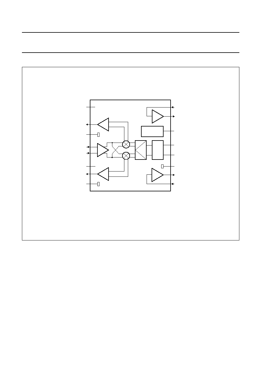
BLOCK DIAGRAM
Fig.1 Block diagram.
handbook, full pagewidth
MGE511
2
0
90
VCO
VOLTAGE
REFERENCE
AMP
AMP
AMP
AMP
AMP
1
2
3
4
5
6
7
8
9
10
11
12
13
14
15
16
VCC(A)
I
GND(D)
RF A
RF B
VCC(D)
Q
GND(A)
Iin
Iout
VCC(V)
VCOB
VCOA
GND(V)
Qout
Qin
TDA8040T
˜
1996 Oct 08
4
Philips Semiconductors
Objective specification
Quadrature demodulator
TDA8040T
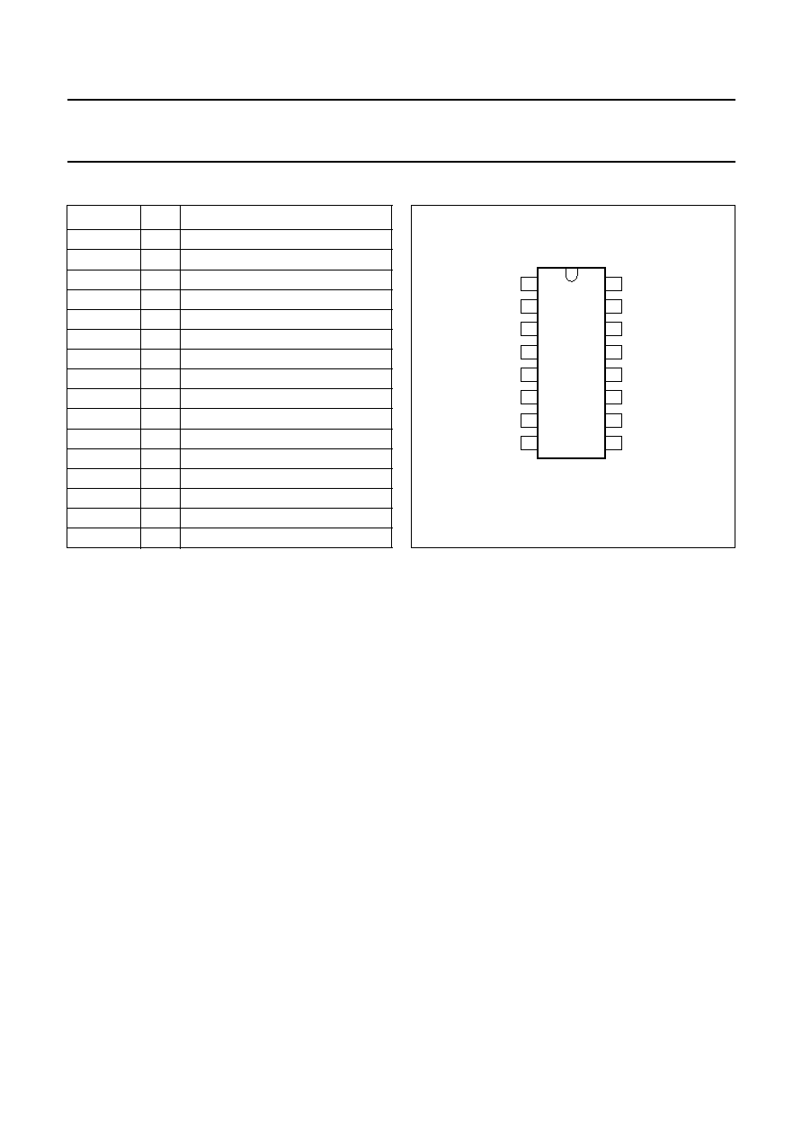
PINNING
SYMBOL
PIN
DESCRIPTION
V
CC(A)
1
supply voltage for I and Q amplifiers
I
2
I channel buffer output
GND(D)
3
demodulator ground
RF A
4
RF input A
RF B
5
RF input B
V
CC(D)
6
supply voltage for demodulator
Q
7
Q channel buffer output
GND(A)
8
I and Q amplifiers ground
Q
in
9
Q channel amplifier input
Q
out
10
Q channel amplifier output
GND(V)
11
VCO ground
VCOA
12
VCO tank circuit A
VCOB
13
VCO tank circuit B
V
CC(V)
14
supply voltage for VCO
I
out
15
I channel amplifier output
I
in
16
I channel amplifier input
Fig.2 Pin configuration.
handbook, halfpage
TDA8040T
MGE510
1
2
3
4
5
6
7
8
16
15
14
13
12
11
10
9
VCC(A)
I
GND(D)
RF A
RF B
VCC(D)
Q
GND(A)
Qin
Qout
GND(V)
VCOA
VCOB
VCC(V)
Iout
Iin
FUNCTIONAL DESCRIPTION
The QPSK modulated RF signal is applied at the input of a
high gain RF amplifier. The amplified signal is then mixed
in a pair of mixers with two LO signals, which are
90 degrees out of phase, to produce the in-phase (I) and
quadrature (Q) signals. These two signals are separately
buffered to drive the external low-pass filters used for the
baseband filtering. The I and Q signals are then amplified
by two matched amplifiers designed to avoid crosstalk
between channels.
The VCO operates at twice the carrier frequency. Its output
signal is applied to a frequency divider (divide-by-2) to
produce the two LO signals which are 90 degrees out of
phase. The VCO is powered from the internal voltage
stabilizer to ensure good shift performance.
1996 Oct 08
5
Philips Semiconductors
Objective specification
Quadrature demodulator
TDA8040T
LIMITING VALUES
In accordance with the Absolute Maximum Rating System (IEC 134).
HANDLING
Inputs and outputs are protected against electrostatic discharge in normal handling. However, to be totally safe, it is
desirable to take normal precautions appropriate to handling MOS devices.
THERMAL CHARACTERISTICS
SYMBOL
PARAMETER
CONDITIONS
MIN.
MAX.
UNIT
V
CC(A)
supply voltage for I and Q amplifiers
-
0.3
+6.0
V
V
CC(D)
supply voltage for demodulator
-
0.3
+6.0
V
V
CC(V)
supply voltage for VCO
-
0.3
+6.0
V
V
n(max)
maximum voltage on all pins
-
0.3
V
CC
V
I
max
maximum sink or source current
-
10
mA
t
sc(max)
maximum short-circuit time on outputs
-
10
s
Z
L(IQ)
AC load impedance for
I and Q channels
f
i
= 15 MHz
35
-
Z
LA(IQ)
AC load impedance for
I and Q output amplifiers
f
i
= 15 MHz
300
-
V
VCO(p-p)
voltage drive level for external oscillator
signal (peak-to-peak value)
-
0.6
V
P
tot
total power dissipation
T
amb
= 70
∞
C
-
500
mW
T
stg
storage temperature
-
55
+150
∞
C
T
j
junction temperature
-
150
∞
C
T
amb
operating ambient temperature
0
70
∞
C
SYMBOL
PARAMETER
VALUE
UNIT
R
th j-a
thermal resistance from junction to ambient in free air
110
K/W