 | –≠–ª–µ–∫—Ç—Ä–æ–Ω–Ω—ã–π –∫–æ–º–ø–æ–Ω–µ–Ω—Ç: TDA9816M | –°–∫–∞—á–∞—Ç—å:  PDF PDF  ZIP ZIP |

DATA SHEET
Preliminary specification
File under Integrated Circuits, IC02
1997 Nov 19
INTEGRATED CIRCUITS
TDA9816M
Multistandard multimedia IF-PLL
and FM radio demodulator

1997 Nov 19
2
Philips Semiconductors
Preliminary specification
Multistandard multimedia IF-PLL and FM
radio demodulator
TDA9816M
FEATURES
∑
5 V supply voltage
∑
Gain controlled wideband Video IF (VIF) amplifier
(AC-coupled)
∑
True synchronous demodulation with active carrier
regeneration (very linear demodulation, good
intermodulation figures, reduced harmonics,
excellent pulse response)
∑
Robustness for over-modulation better than 105% due
to gated phase detector at L/L accent standard and PLL
bandwidth control for negative modulation standards
∑
VCO (Voltage Controlled Oscillator) frequency can be
switched between L and L accent (alignment external)
picture carrier frequency
∑
VIF AGC (Automatic Gain Control) detector for gain
control, operating as peak sync detector for B/G and
peak white detector for L; signal controlled reaction time
for L
∑
Tuner AGC with adjustable TakeOver Point (TOP)
∑
AFC (Automatic Frequency Control) detector without
extra reference circuit
∑
AC-coupled limiting amplifier for sound intercarrier
signal
∑
Alignment-free FM PLL (Phase-Locked Loop)
demodulator with high linearity; integrated de-emphasis
resistor
∑
Integrated level detector
∑
Alignment-free FM radio AFC detector with external
resonator
∑
RIF (Radio IF) amplifier for 10.7 MHz
∑
SIF (Sound IF) input for single reference QSS (Quasi
Split Sound) mode (PLL controlled); SIF AGC detector
for gain controlled SIF amplifier; single reference QSS
mixer able to operate in high performance single
reference QSS mode
∑
AM demodulator without extra reference circuit
∑
Stabilizer circuit for ripple rejection and to achieve
constant output signals
∑
ESD (Electrostatic Discharge) protection for all pins.
GENERAL DESCRIPTION
The TDA9816M is an integrated circuit for multistandard
vision IF signal processing, sound AM and FM
demodulation and FM radio demodulation in multimedia
sets.
ORDERING INFORMATION
TYPE NUMBER
PACKAGE
NAME
DESCRIPTION
VERSION
TDA9816M
SSOP28
plastic shrink small outline package; 28 leads; body width 5.3 mm
SOT341-1
1997 Nov 19
3
Philips Semiconductors
Preliminary specification
Multistandard multimedia IF-PLL and FM
radio demodulator
TDA9816M
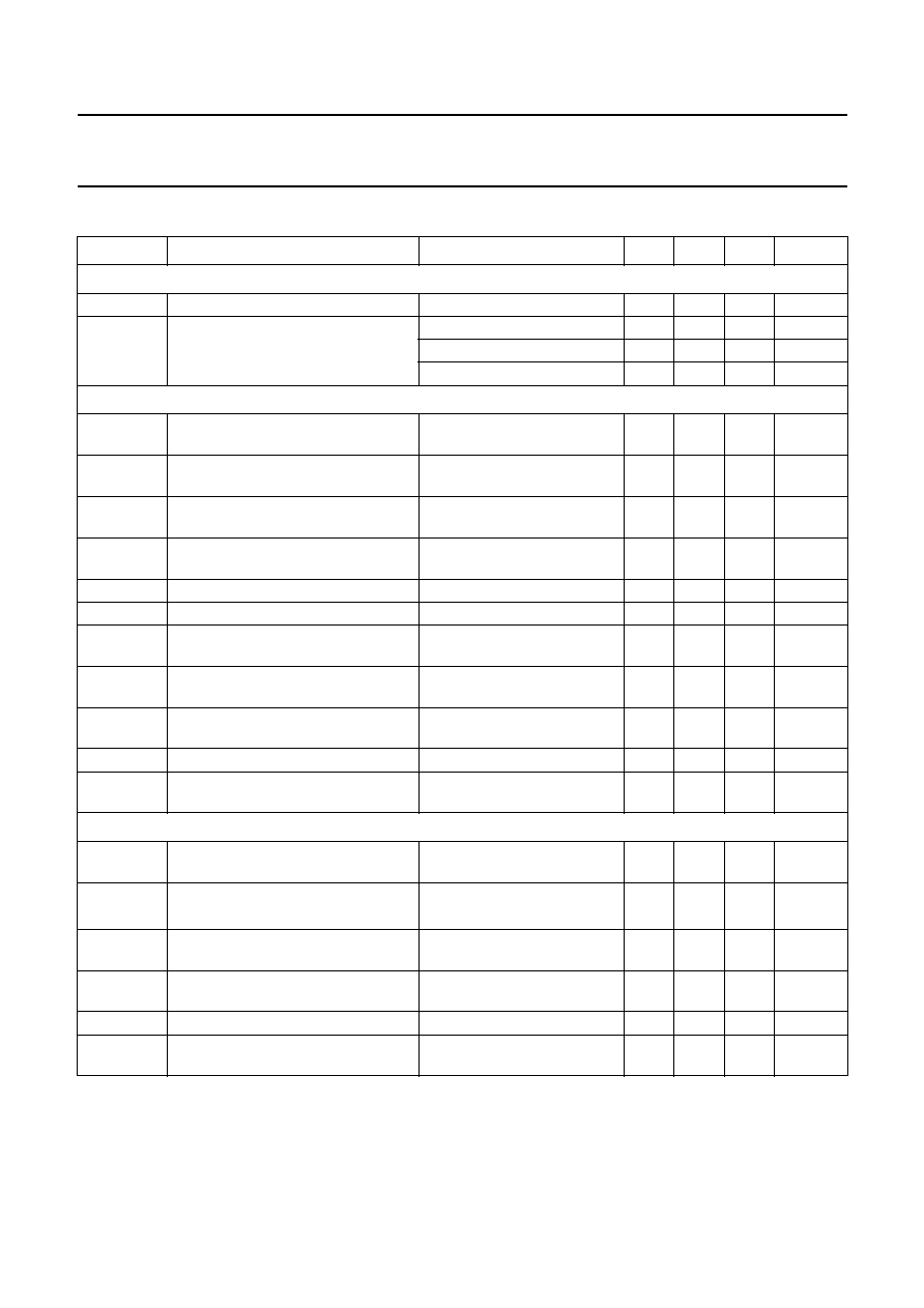
QUICK REFERENCE DATA
Note
1. d
3
is the ratio of the intermodulation product at 10.3 MHz to the level of V
i(4)(max)(rms)
.
SYMBOL
PARAMETER
CONDITIONS
MIN.
TYP.
MAX.
UNIT
Supply (pin 25)
V
P
supply voltage
4.5
5
5.5
V
I
P
supply current
TV mode (B/G standard)
76
89
102
mA
radio mode
29
35
41
mA
power-down mode
5
8
11
mA
Television mode
V
i(VIF)(rms)
minimum vision IF input signal
voltage (RMS value)
-
1 dB video at output
-
60
100
µ
V
V
o(video)(p-p)
video output signal voltage
(peak-to-peak value)
0.97
1.1
1.23
V
B
-
3dB
-
3 dB video bandwidth on pin 18
C
L
< 30 pF; R
L
> 1.5 k
;
AC load
7
8
-
MHz
S/N
W(video)
weighted signal-to-noise ratio for
video
54
58
-
dB
IM(1.1)
intermodulation attenuation at `blue'
f = 1.1 MHz
52
58
-
dB
IM(3.3)
intermodulation attenuation at `blue'
f = 3.3 MHz
52
58
-
dB
H(sup)
suppression of harmonics in video
signal
35
40
-
dB
V
i(SIF)(rms)
minimum sound IF input signal
voltage (RMS value)
-
3 dB at intercarrier output
-
30
70
µ
V
V
o(audio)(rms)
audio output signal voltage for FM
(RMS value)
B/G standard;
27 kHz modulation
0.4
0.5
0.6
V
THD
video
total harmonic distortion for video
27 kHz modulation
-
0.5
1.0
%
S/N
W(audio)
weighted signal-to-noise ratio for
audio
27 kHz modulation; t = 50
µ
s
50
55
-
dB
Radio mode
V
i(RIF)(rms)
minimum radio IF input signal
voltage (RMS value)
d
3
< 60 dB intermodulation;
note 1
-
-
20
mV
V
i(FM)(rms)
minimum FM limiter input signal
voltage (RMS value)
-
100
-
µ
V
V
LD
/log
V
i
output voltage slope according to
FM limiter input voltage
-
50
-
mV/dB
µ
V
V
o(audio)(rms)
audio output signal voltage for radio
(peak-to-peak value)
22.5 kHz modulation
200
250
300
mV
THD
audio
total harmonic distortion for audio
22.5 kHz modulation
-
0.5
1.0
%
S/N
W(audio)
weighted signal-to-noise ratio for
audio
22.5 kHz modulation;
15 kHz bandwidth
59
64
-
dB
S
N
+
N
-------------- unweighted
26 dB
=
1997 Nov 19
4
Philips Semiconductors
Preliminary specification
Multistandard multimedia IF-PLL and FM
radio demodulator
TDA9816M
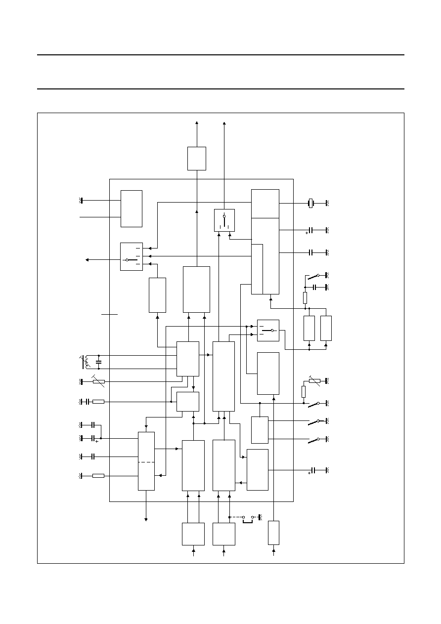
BLOCK DIAGRAM
ok, full pagewidth
1 V (p-p)
MHA990
VCO
TWD
AND TV AFC
QSS MIXER
INTERCARRIER MIXER
AND AM DEMODULATOR
FPLL
SIF AMPLIFIER
RIF AMPLIFIER
AND
AGC DETECTOR
VIF AMPLIFIER
AND
AGC DETECTOR
SIF AMPLIFIER
AND
AGC DETECTOR
TUNER
AGC
VIF
AGC
VIF
SAW
SOUND
TRAP
VIDEO
DEMODULATOR
AND AMPLIFIER
TV AFC
DETECTOR
INTERNAL
VOLTAGE
STABILIZER
GND
n.c.
V
P
AFC/RIF
level
2
◊
f
PC
T
PLL
C
VAGC
TADJ
TV/radio
tuner AGC
1
16
2
LOGIC
4
38
C
DEC
forced
mute
soft mute
threshold
adjust
LP1
LP0
11
LP2
5.5 MHz
13
C
de-em
12
24
15
14
18
10
19
25
22
21
7
5
26
23
V
oAF
1.1 V (p-p)
video
20
TDA9816M
10.7 MHz
10.7 MHz
10.7 MHz
ceramic
resonator
FM-PLL DEMODULATOR AND
AF SIGNAL PROCESSING
LEVEL DETECTOR
RADIO
AFC
intercarrier
mode
C
SAGC
6
SIF
SAW
V
iVIF1
V
iVIF2
V
iSIF1
V
iSIF2
V
iRIF
V
oQSS
V
iFM
28
27
17
9
C
BL
L accent
adjust
Fig.1 Block diagram.

1997 Nov 19
5
Philips Semiconductors
Preliminary specification
Multistandard multimedia IF-PLL and FM
radio demodulator
TDA9816M
PINNING
SYMBOL
PIN
DESCRIPTION
V
iVIF1
1
VIF differential input signal voltage 1
V
iVIF2
2
VIF differential input signal voltage 2
LP0
3
logic port 0
V
iRIF
4
RIF input
C
VAGC
5
VIF AGC capacitor
C
SAGC
6
SIF AGC capacitor
T
PLL
7
PLL loop filter
LP1
8
logic port 1
LADJ
9
L/L accent switch and adjustment
V
oAF
10
audio output
LP2
11
logic port 2 and soft mute threshold
adjustment
C
de-em
12
de-emphasis capacitor
C
DEC
13
decoupling capacitor
V
oQSS
14
single reference QSS/intercarrier
output voltage
V
iFM
15
sound intercarrier input voltage
TAGC
16
TV/radio tuner AGC output
C
BL
17
black level detector
V
o(vid)
18
composite video output voltage
AFC
19
AFC/RIF level output
n.c.
20
not connected
VCO1
21
VCO1 resonance circuit
VCO2
22
VCO2 resonance circuit
GND
23
ground
CERRES
24
ceramic resonator 10.7 MHz
V
P
25
supply voltage
TADJ
26
tuner AGC takeover point adjustment
V
iSIF1
27
SIF differential input signal voltage 1
V
iSIF2
28
SIF differential input signal voltage 2
Fig.2 Pin configuration.
handbook, halfpage
ViVIF1
ViVIF2
LP0
ViRIF
CVAGC
CSAGC
TPLL
LP1
LADJ
VoAF
LP2
Cde-em
CDEC
VoQSS
ViSIF2
ViSIF1
TADJ
VP
GND
VCO2
CERRES
VCO1
n.c.
AFC
Vo(vid)
CBL
TAGC
ViFM
1
2
3
4
5
6
7
8
9
10
11
12
13
28
27
26
25
24
23
22
21
20
19
18
17
16
15
14
TDA9816M
MHA989