2000 Feb 18
2
Philips Semiconductors
Product specification
Speech circuit with dialler interface, regulated
supply and earpiece volume control
TEA1111A
FEATURES
∑
Low DC line voltage; operates down to 1.5 V (excluding
voltage drop across external polarity guard)
∑
Line voltage regulator with adjustable DC voltage
∑
3.25 V regulated strong supply point for peripheral
circuits compatible with:
≠ Speech mode
≠ Ringer mode
≠ Trickle mode.
∑
Transmit stage with:
≠ Microphone amplifier with symmetrical high
impedance inputs
≠ DTMF amplifier with confidence tone on earpiece.
∑
Receive stage with:
≠ Earpiece amplifier with adjustable gain and volume
control.
∑
MUTE input for pulse or DTMF dialling
∑
AGC line loss compensation for microphone and
earpiece
∑
LED control output.
APPLICATIONS
∑
Line powered telephone sets with LCD module
∑
Cordless telephones
∑
Fax machines
∑
Answering machines.
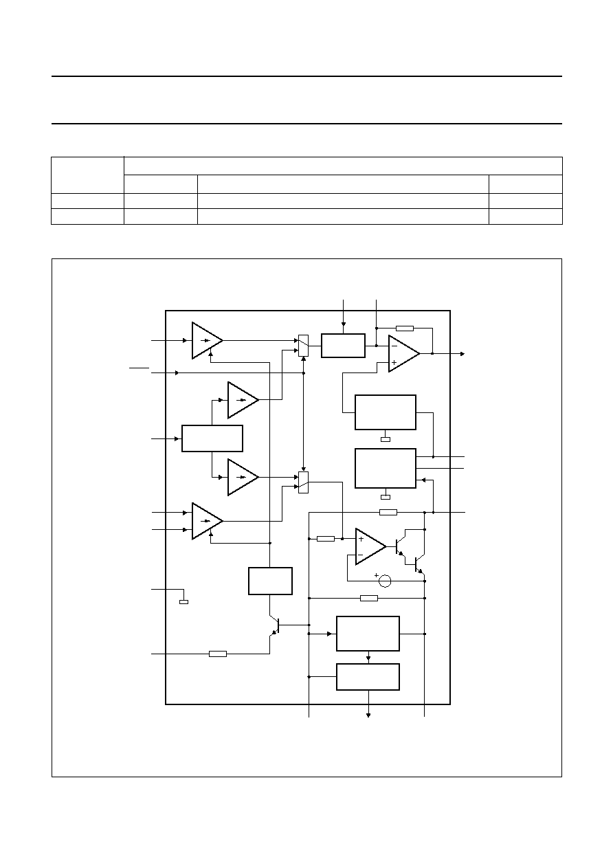
GENERAL DESCRIPTION
The TEA1111A is a bipolar integrated circuit that performs
all speech and line interface functions required in fully
electronic telephone sets. It performs electronic switching
between speech and dialling. The IC operates at a line
voltage down to 1.5 V DC (with reduced performance) to
facilitate the use of telephone sets connected in parallel.
When the line current is high enough, a fixed amount of
current is derived from the LN pin in order to create a
strong supply point at pin V
DD
. The voltage at pin V
DD
is
regulated to 3.25 V to supply peripherals such as dialler,
LCD module and microcontroller.
QUICK REFERENCE DATA
I
line
= 15 mA; V
EE
= 0 V; V
VCI
= 0 V; R
SLPE
= 20
; AGC pin connected to V
EE
; Z
line
= 600
; f = 1 kHz; measured
according to test circuits given in Figs 15, 16 and 17; T
amb
= 25
∞
C; T
j
= 25
∞
C for TEA1111AUH; unless otherwise
specified.
SYMBOL
PARAMETER
CONDITIONS
MIN.
TYP.
MAX. UNIT
I
line
line current operating range
normal operation
11
-
140
mA
with reduced
performance
1
-
11
mA
V
LN
DC line voltage
3.7
4.0
4.3
V
I
CC
internal current consumption
V
CC
= 3.3 V
-
1.15
1.4
mA
V
CC
supply voltage for internal circuitry (unregulated)
I
P
= 0 mA
-
3.3
-
V
V
DD
regulated supply voltage for peripherals
speech mode
I
DD
=
-
3 mA
2.95
3.25
3.55
V
ringer mode
I
DD
= 75 mA
3.0
3.3
3.6
V
I
DD
available supply current for peripherals
-
-
-
3
mA
G
v(TX)
typical voltage gain for microphone amplifier
V
MIC
= 4 mV (RMS)
43.2
44.2
45.2
dB
G
v(QR)
typical voltage gain for earpiece amplifier
V
IR
= 4 mV (RMS)
26.4
27.4
28.4
dB
G
v(QR)
volume control range for earpiece amplifier
0
14.5
-
dB
G
v(trx)
gain control range for microphone and earpiece
amplifiers with respect to I
line
= 15 mA
I
line
= 85 mA
-
6.0
-
dB
G
v(trx)(m)
gain reduction for microphone and earpiece
amplifiers
MUTE = LOW
-
80
-
dB
2000 Feb 18
4
Philips Semiconductors
Product specification
Speech circuit with dialler interface, regulated
supply and earpiece volume control
TEA1111A
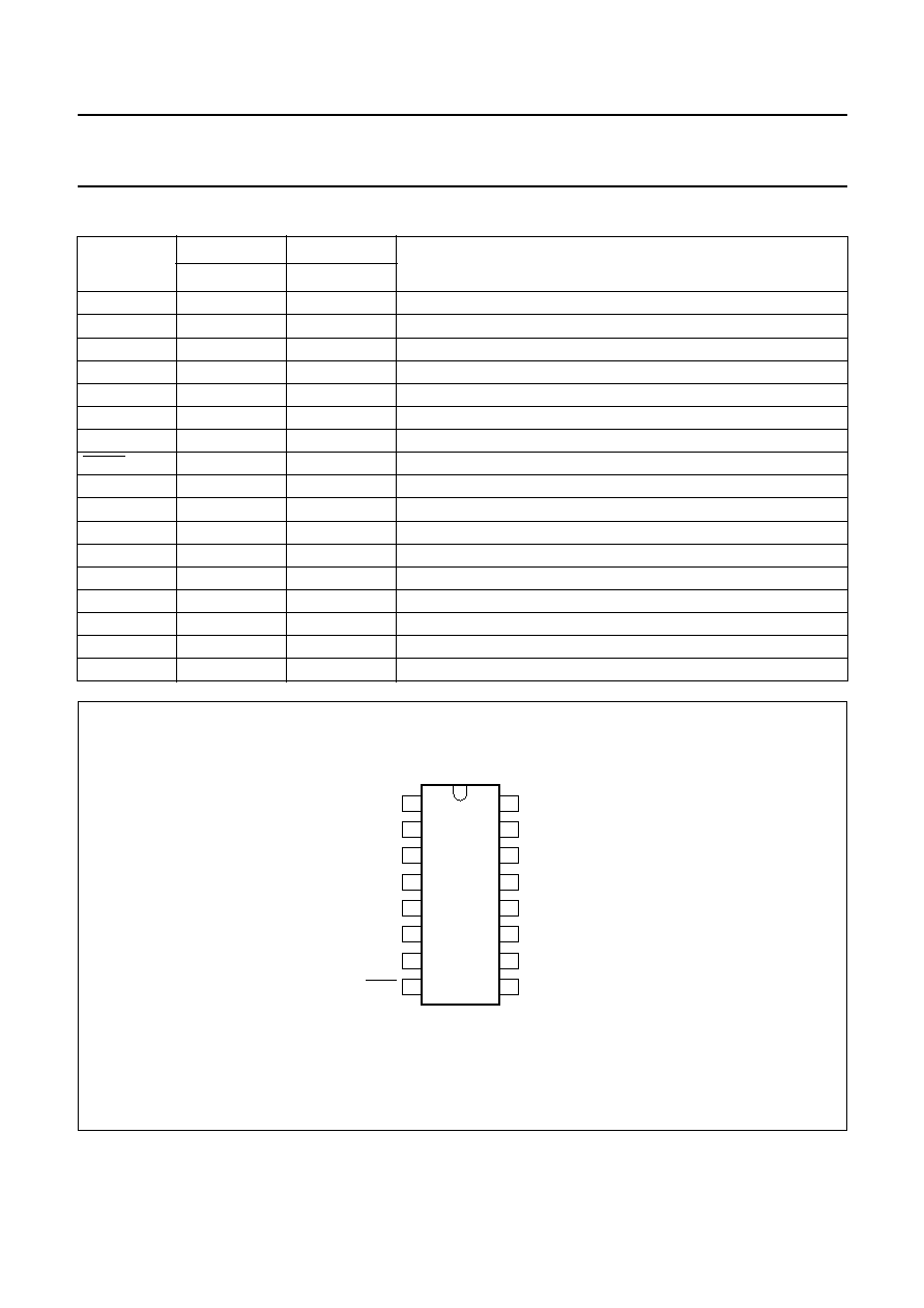
PINNING
SYMBOL
PIN
PAD
DESCRIPTION
TEA1111TV
TEA1111AUH
LN
1
1
positive line terminal
SLPE
2
2
slope (DC resistance) adjustment
REG
3
3
line voltage regulator decoupling
IR
4
4
receive amplifier input
AGC
5
5
automatic gain control/ line loss compensation
DTMF
6
6
dual-tone multi-frequency input
V
DD
7
7
regulated supply for peripherals
MUTE
8
8
mute input to select speech or dialling mode (active LOW)
n.c.
-
9
not connected
VCI
9
10
volume control input
V
EE
10
11, 12
negative line terminal
QR
11
13
earpiece amplifier output
GAR
12
14
earpiece amplifier gain adjustment
MIC+
13
15
non-inverting microphone amplifier input
MIC
-
14
16
inverting microphone amplifier input
LEDC
15
17
LED control output
V
CC
16
18
supply voltage for internal circuit
handbook, halfpage
TEA1111A
FCA052
1
2
3
4
5
6
7
8
16
15
14
13
12
11
10
9
LN
SLPE
REG
IR
AGC
DTMF
VDD
MUTE
VCI
VEE
QR
GAR
MIC
+
MIC
-
VCC
LEDC
Fig.2 Pin configuration.

2000 Feb 18
5
Philips Semiconductors
Product specification
Speech circuit with dialler interface, regulated
supply and earpiece volume control
TEA1111A
FUNCTIONAL DESCRIPTION
All data given in this chapter concerns typical values,
except when otherwise specified.
Supply (pins LN, SLPE, REG, V
CC
and V
DD
)
The supply for the TEA1111A and its peripherals is
obtained from the telephone line (see Fig.3).
T
HE LINE INTERFACE
(
PINS
LN, SLPE
AND
REG)
The IC generates a stabilized reference voltage (V
ref
)
across pins LN and SLPE. V
ref
is temperature
compensated and can be adjusted by using an external
resistor (R
VA
). V
ref
equals 3.8 V and can be increased by
connecting R
VA
between pins REG and SLPE or
decreased by connecting R
VA
between pins REG and LN.
The voltage at pin REG is used by the internal regulator to
generate V
ref
and is decoupled by C
REG
, which is
connected to V
EE
. This capacitor, converted to an
equivalent inductance, (see Section "Set impedance")
determines the set impedance conversion from its DC
value (R
SLPE
) to its AC value (R
CC
in the audio-frequency
range). The voltage at pin SLPE is proportional to the line
current.
The voltage at pin LN is:
V
LN
= V
ref
+ R
SLPE
◊
I
SLPE
I
SLPE
= I
line
-
I
CC
-
I
P
-
I
SUP
-
I
LEDC
where:
I
line
= line current
I
CC
= current consumption of the IC
I
P
= supply current for external circuits
I
SUP
= current consumed between LN and V
EE
by the
V
DD
regulator
I
LEDC
= supply current for external LED circuitry.
The preferred value for R
SLPE
is 20
. Changing R
SLPE
will
affect more than the DC characteristics; it also influences
the microphone and DTMF gains, the gain control
characteristics, the sidetone level and the maximum
output swing on the line.
The DC line current flowing into the set is determined by
the exchange supply voltage (V
EXCH
), the feeding bridge
resistance (R
EXCH
), the DC resistance of the telephone
line (R
line
) and the reference voltage (V
ref
). With line
currents below I
low
(9 mA), the internal reference voltage
(generating V
ref
) is automatically adjusted to a lower value.
This means that several sets can operate in parallel with
DC line voltages (excluding the polarity guard) down to an
absolute minimum voltage of 1.5 V. At line currents below
I
low
, the circuit has limited sending and receiving levels.
This is called the low voltage area.
T
HE INTERNAL SUPPLY POINT
(
PIN
V
CC
)
The internal circuitry of the TEA1111A is supplied from
pin V
CC
. This voltage supply is derived from the line
voltage by means of a resistor (R
CC
) and must be
decoupled by a capacitor C
VCC
. It may also be used to
supply some external circuits.
The V
CC
voltage (see also Figs 4 and 5) depends on the
current consumed by the IC and the peripheral circuits as:
V
CC0
= V
LN
-
R
CC
◊
I
CC
V
CC
= V
CC0
-
R
CC
◊
(I
P
+ I
rec
)
Where I
rec
is the current consumed by the output stage of
the earpiece amplifier.