 | –≠–ª–µ–∫—Ç—Ä–æ–Ω–Ω—ã–π –∫–æ–º–ø–æ–Ω–µ–Ω—Ç: TEA6330T | –°–∫–∞—á–∞—Ç—å:  PDF PDF  ZIP ZIP |

DATA SHEET
Preliminary specification
Supersedes data of June 1991
File under Integrated Circuits, IC01
January 1992
INTEGRATED CIRCUITS
TEA6330T
Sound fader control circuit
for car radios

January 1992
2
Philips Semiconductors
Preliminary specification
Sound fader control circuit
for car radios
TEA6330T
FEATURES
∑
Stereo/hi-fi processor for car radios performed with
volume, balance, bass and treble controls
∑
Sound fader control (front/rear) down to
-
30 dB in steps
of 2 dB
∑
Fast muting via bus or via setting the muting pin
∑
Suitable for external audio equalizers, can be looped-in
controlled by the I
2
C-bus
∑
Power-on reset on chip sets the device into general
mute position
∑
AC and DC short-circuit protected concerning
neighbouring pins
∑
I
2
C-bus control for all functions.
GENERAL DESCRIPTION
This bipolar IC is an I
2
C-bus controlled sound/volume
controller for car radios, in addition with fader function and
the possibility of an external equalizer.
QUICK REFERENCE DATA
ORDERING INFORMATION
Note
1. Plastic small outline package; 20 leads; body width 7.5 mm; (SOT163A); SOT163-1; 1996 August 02.
SYMBOL
PARAMETER
MIN.
TYP.
MAX.
UNIT
V
P
supply voltage
7
8.5
10
V
I
P
supply current
-
26
-
mA
V
i
maximum AF input signal
(RMS value)
2
-
-
V
V
o
maximum AF output signal
(RMS value)
1.1
-
-
V
G
v
volume control range, separated
-
66
-
+
20
dB
fader control range, separated
0
-
-
30
dB
bass control range
-
12
-
+
15
dB
treble control range
-
12
-
+
12
dB
THD
total harmonic distortion
-
-
0.2
%
S/N(W)
weighted signal-to-noise ratio
-
67
-
dB
CR
crosstalk attenuation
-
90
-
dB
B
frequency response (
-
1 dB)
35 to
-
20000
-
Hz
EXTENDED
TYPE NUMBER
PACKAGE
PINS
PIN POSITION
MATERIAL
CODE
TEA6330T
(1)
20
SO
plastic
SOT163A

January 1992
3
Philips Semiconductors
Preliminary specification
Sound fader control circuit
for car radios
TEA6330T
Fig.1 Block and test circuit.
Fig.2
Connection of equalizer (Table 7).
In application with equalizer circuit
TEA6360 coupling capacitors are not
necessary. Connectors for RIGHT in
brackets.
Fig.3
T-filter for enhanced bass control (Fig.5).
Connectors for LEFT in brackets.
January 1992
4
Philips Semiconductors
Preliminary specification
Sound fader control circuit
for car radios
TEA6330T
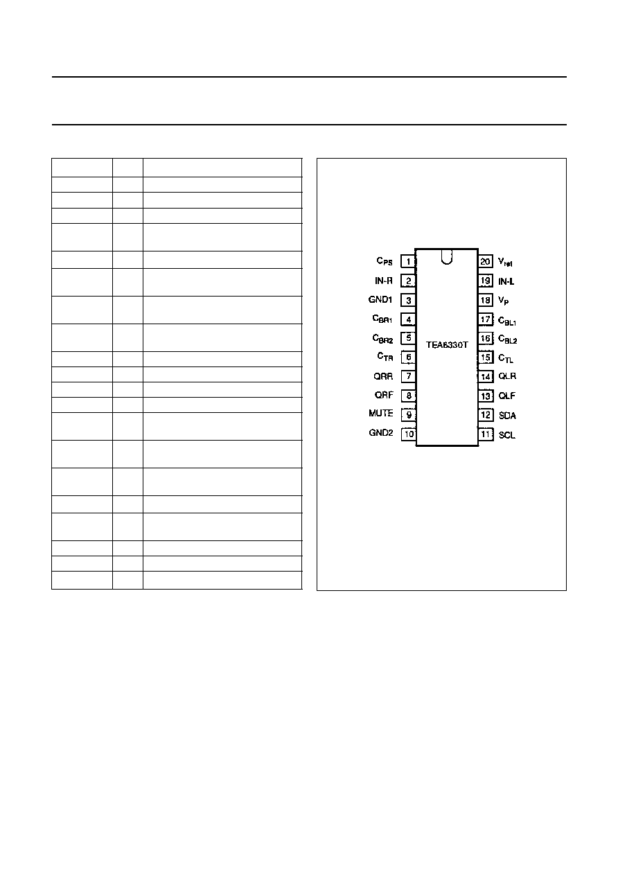
PINNING
SYMBOL
PIN
DESCRIPTION
C
PS
1
filtering capacitor for power supply
IN-R
2
audio input signal RIGHT
GND1
3
analog ground (0 V)
C
BR1
4
capacitor for bass control RIGHT
and signal to equalizer
C
BR2
5
capacitor for bass control RIGHT
C
TR
6
capacitor for treble control RIGHT,
input signal for equalizer RIGHT
QRR
7
right audio output signal of rear
channel
QRF
8
right audio output signal of front
channel
MUTE
9
input to set mute externally
GND2
10
digital ground (0 V) for bus control
SCL
11
clock signal of I
2
C-bus
SDA
12
data signal of I
2
C-bus
QLF
13
left audio output signal of front
channel
QLR
14
left audio output signal of rear
channel
C
TL
15
capacitor for treble control LEFT,
input signal for equalizer LEFT
C
BL2
16
capacitor for bass control LEFT
C
BL1
17
capacitor for bass control LEFT
and signal to equalizer
V
P
18
+
8.5 V supply voltage
IN-L
19
audio input signal LEFT
V
ref
20
reference voltage output (V
P
/2)
Fig.4 Pin configuration.
January 1992
5
Philips Semiconductors
Preliminary specification
Sound fader control circuit
for car radios
TEA6330T
FUNCTIONAL DESCRIPTION
This bipolar IC is an I
2
C-bus controlled sound/volume
controller for car radios including fader function and the
possibility of an external equalizer. The sound signal
setting is performed by resistor chains in combination with
multi-input operational amplifiers. The advantages of this
principle are the combination of low noise, low distortion
and a high dynamic range. The separated volume controls
of the left and the right channel make the balance control
possible. The value and the characteristic of the balance is
controlled via the I
2
C-bus.
The contour function is performed by setting an extra bass
control and optional treble, depending on the actual
volume position. Its switching points and its range are also
controllable via the I
2
C-bus.
An interface is assigned behind the volume control to
loop-in an equalizer (Fig.2). In this case the treble control
is switched off, and the bass control can be used to set the
contour.
Low level control fader is included independent of the
volume controls, because the TEA6330T has four driver
outputs (for front and rear).
An extra mute position for the front, the rear or for all
channels is built in. The last function may be used for
muting during preset selection. No external interface is
required between the microcomputer and this circuit, for all
switching and controlling functions are controllable via the
two-wire I
2
C-bus.
The separate mute-pin allows to switch the fader into mute
position without using the I
2
C-bus.
The on chip power-on reset sets the TEA6330T into the
general mute mode.
LIMITING VALUES
In accordance with the Absolute Maximum System (IEC 134). Ground pins 3 and 10 connected together.
* Equivalent to discharging a 200 pF capacitor through a 0
series resistor.
** Equivalent to discharging a 100 pF capacitor through a 1.5 k
series resistor.
SYMBOL
PARAMETER
MIN.
MAX.
UNIT
V
P
supply voltage (pin 18)
0
10
V
P
tot
total power dissipation
0
700
mW
T
stg
storage temperature range
-
55
150
∞
C
T
amb
operating ambient temperature range
-
40
85
∞
C
V
ESD
electrostatic handling* for all pins
-
±
300
V
electrostatic handling** for all pins
-
±
4000
V
January 1992
6
Philips Semiconductors
Preliminary specification
Sound fader control circuit
for car radios
TEA6330T
CHARACTERISTICS
V
P
= 8.5 V; load resistors at audio outputs 10 k
, f
i
= 1 kHz (R
S
= 600
), bass and treble in linear position, fader in off
position and T
amb
= 25
∞
C; measurements taken in Fig.1 unless otherwise specified.
SYMBOL
PARAMETER
CONDITIONS
MIN.
TYP.
MAX.
UNIT
V
P
supply voltage range (pin 18)
7
8.5
10
V
I
P
supply current
-
26
-
mA
V
ref
reference voltage (pin 20)
0.45 V
P
0.5 V
P
0.55 V
P
V
V
O
DC voltage at output (pins 7, 8, 13, 14)
-
0.5 V
P
-
V
Measurements over all
V
i
maximum AF input level for THD = 2 %
G
v
=
-
66 to
-
6 dB
at pins 2 and 19 (RMS value)
and V
P
= 8.1 V
2
-
-
V
V
o
maximum AF output level for THD = 2%
G
v
=
-
4 to
+
20 dB
at pins 7, 8, 13, 14 (RMS value)
and V
P
= 8.1 V
1.1
-
-
V
G
v
maximum gain by volume setting
19
20
21
dB
B
frequency response
-
1 dB roll-off frequency
35 to
-
20000
-
Hz
CR
crosstalk attenuation
f = 250 to 10000 Hz
G
v
= 0 dB
70
90
-
dB
THD
total harmonic distortion
f = 20 to 12500 Hz
V
i (RMS)
= 50 mV
G
v
=
+
20 dB
-
0.1
0.3
%
V
i (RMS)
= 500 mV
G
v
= 0 dB
-
0.05
0.2
%
V
i (RMS)
= 1.6 V
G
v
=
-
10 dB
-
0.2
0.5
%
RR
ripple rejection for V
R
<
200 mV RMS
G
v
= 0 dB
f = 100 Hz
-
70
-
dB
f = 40 Hz to 3 kHz
-
60
-
dB
f = 3 to 12.5 kHz
-
50
-
dB
P
N
noise power at output of a 25 W
powerstage with 26 dB gain
(only contribution of TEA6330T)
mute position
(V
9
= 0)
-
-
10
nW
BUS
crosstalk attenuation between SDA, SCL
and signal output
G
v
= 0 dB
-
110
-
dB
(20 log V
BUS
(p-p)/V
o
RMS)
S/N(W)
weighted signal-to-noise ratio for
CCIR 468-2 quasi
peak for 6 W power
amplifier
V
i
= 50 mV RMS
P
o
= 50 mW
-
65
-
dB
V
i
= 500 mV RMS
P
o
= 50 mW
-
67
-
dB
V
i
= 50 mV RMS
P
o
= 1 W
65
72
-
dB
V
i
= 500 mV RMS
P
o
= 1 W
71
78
-
dB
V
i
= 50 mV RMS
P
o
= 6 W; Fig.9
-
72
-
dB
V
i
= 500 mV RMS
P
o
= 6 W; Fig.9
-
86
-
dB

January 1992
7
Philips Semiconductors
Preliminary specification
Sound fader control circuit
for car radios
TEA6330T
Audio frequency outputs QLF, QRF, QLR and QRR
V
o
maximum output signal (RMS value)
1.1
-
-
V
R
o
output resistance (pins 7, 8, 13 and 14)
-
100
150
R
L
admissible output load resistor
to ground or V
CC
7.5
-
-
k
C
L
admissible output load capacitor
-
-
2.5
nF
V
N(W)
weighted noise voltage at output
CCIR 468-2 ; Fig.8
quasi peak
for maximum gain
G
v
=
+
20 dB
-
110
220
µ
V
for 0 dB gain
G
v
= 0 dB
-
25
50
µ
V
for minimum gain
G
v
=
-
66 dB
-
19
38
µ
V
for mute position
(V
9
= 0)
-
11
22
µ
V
Volume control
R
G
= 600
R
l
input resistance (pins 2 and 19)
35
50
65
k
G
v
volume control range
Table 2
-
66
-
+
20
dB
G
v
step width
-
2
-
dB
gain set error
G
v
=
-
50 to
+
20 dB
-
-
2
dB
G
v
=
-
66 to
-
50 dB
-
-
3
dB
gain tracking error
balance in mid position
-
-
2
dB
mute
mute attenuation at volume mute
set mute-bits
76
90
-
dB
Bass control
G
v
controllable bass range
Table 3; Fig.6
maximum boost
f = 40 Hz
14
15
16
dB
maximum boost
f = 100 Hz
12
13
14
dB
maximum attenuation
f = 40 Hz
11
12
13
dB
maximum attenuation
f = 100 Hz
10
11
12
dB
G
v
step width
f = 40 Hz
2.5
3
3.5
dB
Treble control
G
v
controllable treble range
Table 4; Fig.7
maximum boost
f = 10 kHz
9
10
11
dB
maximum boost
f = 15 kHz
11
12
13
dB
maximum boost
f
>
15 kHz
-
-
15
dB
maximum attenuation
f = 10 kHz
9
10
11
dB
maximum attenuation
f = 15 kHz
11
12
13
dB
G
v
step width
f = 15 kHz
2.5
3
3.5
dB
SYMBOL
PARAMETER
CONDITIONS
MIN.
TYP.
MAX.
UNIT
January 1992
8
Philips Semiconductors
Preliminary specification
Sound fader control circuit
for car radios
TEA6330T
Fader control
G
v
fader control range
Table 5
0 to
-
-
30
-
dB
step width
1.5
2
2.5
dB
MUTE
mute attenuation
GMB-bit = 1; Table 6
74
84
-
dB
V
o
DC offset output voltage (pins 7, 8, 13,
14)
between any adjoining volume step
and any step to mute
G
v
=
-
66 to 0 dB
-
0.2
10
mV
G
v
= 0 to
+
20 dB
-
2
15
mV
in any treble and fader position
G
v
=
-
66 to 0 dB
-
-
10
mV
in any bass position
G
v
=
-
66 to 0 dB
-
-
10
mV
External mute (pin 9)
V
9
input voltage for MUTE-ON (LOW)
fader is switched into
general mute position
0
-
1.5
V
input voltage for MUTE-OFF (HIGH)
Tables 2 and 5
3
-
V
P
V
input voltage for MUTE-OFF
pin 9 open-circuit
-
5
-
V
I
9
input current
-
-
±
10
µ
A
I
2
C-bus, SCL and SDA (pins 11 and 12)
V
11, 12
input voltage HIGH-level
3
-
V
P
V
input voltage LOW-level
0
-
1.5
V
I
11, 12
input current
-
-
±
10
µ
A
V
ACK
output voltage at acknowledge (pin 12)
I
12
=
-
3 mA
-
-
0.4
V
Power-on reset, when reset is active the GMU-bit (general mute) is set and the bus receiver is in reset position
V
P
supply voltage for start of reset
increasing voltage
-
-
2.5
V
supply voltage for end of reset
increasing voltage
5.2
6.0
6.8
V
supply voltage for start of reset
decreasing voltage
4.2
5.0
5.8
V
SYMBOL
PARAMETER
CONDITIONS
MIN.
TYP.
MAX.
UNIT

January 1992
9
Philips Semiconductors
Preliminary specification
Sound fader control circuit
for car radios
TEA6330T
Fig.5 Bass control with enhanced control range (T-filter coupling, Fig.1).
Fig.6 Bass control with normal control range (Fig.1).

January 1992
10
Philips Semiconductors
Preliminary specification
Sound fader control circuit
for car radios
TEA6330T
Fig.7 Treble control.
Fig.8 Noise voltage on outputs (CCIR 468-2 weighted, quasi-peak).

January 1992
11
Philips Semiconductors
Preliminary specification
Sound fader control circuit
for car radios
TEA6330T
Fig.9
Signal-to-noise ratio (CClR 468-2 weighted, quasi-peak) for TEA6330T with a 6 W power amplifier
(20 dB gain, Fig.10). Measurements without noise contribution of the power amplifier.
Fig.10 Signal-to-noise ratio measurement (Fig.9) with V
i
= 50 mV RMS, V
o
= 500 mV RMS for P
max
= 6 W.

January 1992
12
Philips Semiconductors
Preliminary specification
Sound fader control circuit
for car radios
TEA6330T
I
2
C-BUS PROTOCOL
I
2
C-bus format
If more than 1 byte DATA are transmitted, then auto-increment of the subaddress is performed.
Byte organisation
Table 1 I
2
C-bus transmission
Function of the bits:
S
SLAVE ADDRESS
A
SUBADDRESS
A
DATA
P
S
=
start condition
SLAVE ADDRESS
=
1000 000X
A
=
acknowledge, generated by the slave
SUBADDRESS
=
subaddress byte, Table 1
DATA
=
data byte, Table 1
P
=
stop condition
X
=
read/write control bit
X = 0, order to write (the circuit is slave receiver only)
FUNCTION
SUBADDRESS BYTE
DATA BYTE
D7
D6
D5
D4
D3
D2
D1
D0
volume left
0
0
0
0
0
0
0
0
0
0
VL5
VL4
VL3
VL2
VL1
VL0
volume right
0
0
0
0
0
0
0
1
0
0
VR5
VR4
VR3
VR2
VR1
VR0
bass
0
0
0
0
0
0
1
0
0
0
0
0
BA3
BA2
BA1
BA0
treble
0
0
0
0
0
0
1
1
0
0
0
0
TR3
TR2
TR1
TR0
fader
0
0
0
0
0
1
0
0
0
0
MFN
FCH
FA3
FA2
FA1
FA0
audio switch
0
0
0
0
0
1
0
1
GMU
EQN
0
0
0
0
0
0
VL0
to
VL5
volume control of left channel (balance control)
VR0
to
VR5
volume control of right channel (balance control)
BA0
to
BA3
bass control of both channels
TRO
to
TR3
treble control of both channels
FA0
to
FA3
fader control front to rear
FCH
select fader channels front or rear
MFN
mute control of the selected channels front or rear
GMU
mute control, general mute
EQN
equalizer switchover (0 = equalizer-on)

January 1992
13
Philips Semiconductors
Preliminary specification
Sound fader control circuit
for car radios
TEA6330T
Table 2(a) Volume setting LEFT
G
V
DATA
DB
VL5
VL4
VL3
VL2
VL1
VL0
+
20
1
1
1
1
1
1
+
18
1
1
1
1
1
0
+
16
1
1
1
1
0
1
+
14
1
1
1
1
0
0
+
12
1
1
1
0
1
1
+
10
1
1
1
0
1
0
+
8
1
1
1
0
0
1
+
6
1
1
1
0
0
0
+
4
1
1
0
1
1
1
+
2
1
1
0
1
1
0
0
1
1
0
1
0
1
-
2
1
1
0
1
0
0
-
4
1
1
0
0
1
1
-
6
1
1
0
0
1
0
-
8
1
1
0
0
0
1
-
10
1
1
0
0
0
0
-
12
1
0
1
1
1
1
-
14
1
0
1
1
1
0
-
16
1
0
1
1
0
1
-
18
1
0
1
1
0
0
-
20
1
0
1
0
1
1
-
22
1
0
1
0
1
0
-
24
1
0
1
0
0
1
-
26
1
0
1
0
0
0
-
28
1
0
0
1
1
1
-
30
1
0
0
1
1
0
-
32
1
0
0
1
0
1
-
34
1
0
0
1
0
0
-
36
1
0
0
0
1
1
-
38
1
0
0
0
1
0
-
40
1
0
0
0
0
1
-
42
1
0
0
0
0
0
-
44
0
1
1
1
1
1
-
46
0
1
1
1
1
0
-
48
0
1
1
1
0
1
-
50
0
1
1
1
0
0
-
52
0
1
1
0
1
1
-
54
0
1
1
0
1
0
-
56
0
1
1
0
0
1
-
58
0
1
1
0
0
0
-
60
0
1
0
1
1
1
-
62
0
1
0
1
1
0
-
64
0
1
0
1
0
1
-
66
0
1
0
1
0
0
mute
left
0
1
0
0
1
1
mute
left
0
1
0
0
1
0
---
---
---
---
---
---
---
---
---
mute
left
0
0
0
0
0
0
G
V
DATA
DB
VL5
VL4
VL3
VL2
VL1
VL0

January 1992
14
Philips Semiconductors
Preliminary specification
Sound fader control circuit
for car radios
TEA6330T
Table 2(b) Volume setting RIGHT
G
V
DATA
DB
VR5
VR4
VR3
VR2
VR1
VL0
+
20
1
1
1
1
1
1
+
18
1
1
1
1
1
0
+
16
1
1
1
1
0
1
+
14
1
1
1
1
0
0
+
12
1
1
1
0
1
1
+
10
1
1
1
0
1
0
+
8
1
1
1
0
0
1
+
6
1
1
1
0
0
0
+
4
1
1
0
1
1
1
+
2
1
1
0
1
1
0
0
1
1
0
1
0
1
-
2
1
1
0
1
0
0
-
4
1
1
0
0
1
1
-
6
1
1
0
0
1
0
-
8
1
1
0
0
0
1
-
10
1
1
0
0
0
0
-
12
1
0
1
1
1
1
-
14
1
0
1
1
1
0
-
16
1
0
1
1
0
1
-
18
1
0
1
1
0
0
-
20
1
0
1
0
1
1
-
22
1
0
1
0
1
0
-
24
1
0
1
0
0
1
-
26
1
0
1
0
0
0
-
28
1
0
0
1
1
1
-
30
1
0
0
1
1
0
-
32
1
0
0
1
0
1
-
34
1
0
0
1
0
0
-
36
1
0
0
0
1
1
-
38
1
0
0
0
1
0
-
40
1
0
0
0
0
1
-
42
1
0
0
0
0
0
-
44
0
1
1
1
1
1
-
46
0
1
1
1
1
0
-
48
0
1
1
1
0
1
-
50
0
1
1
1
0
0
-
52
0
1
1
0
1
1
-
54
0
1
1
0
1
0
-
56
0
1
1
0
0
1
-
58
0
1
1
0
0
0
-
60
0
1
0
1
1
1
-
62
0
1
0
1
1
0
-
64
0
1
0
1
0
1
-
66
0
1
0
1
0
0
mute
right
0
1
0
0
1
1
mute
right
0
1
0
0
1
0
---
---
---
---
---
---
---
---
---
mute
right
0
0
0
0
0
0
G
V
DATA
DB
VR5
VR4
VR3
VR2
VR1
VL0

January 1992
15
Philips Semiconductors
Preliminary specification
Sound fader control circuit
for car radios
TEA6330T
Table 3(a)
Bass setting with equalizer passive (EQN =1)
G
V
DATA
DB
D3
D2
D1
D0
+15
1
1
1
1
+15
1
1
1
0
+15
1
1
0
1
+15
1
1
0
0
+12
1
0
1
1
+9
1
0
1
0
+6
1
0
0
1
+3
1
0
0
0
0
0
1
1
1
-
3
0
1
1
0
-
6
0
1
0
1
-
9
0
1
0
0
-
12
0
0
1
1
-
12
0
0
1
0
-
12
0
0
0
0
Table 3(b)
Bass setting with equalizer active (EQN = 0)
G
V
DATA
DB
D3
D2
D1
D0
+
15
1
1
1
1
+
15
1
1
1
0
+
15
1
1
0
1
+
15
1
1
0
0
+
12
1
0
1
1
+
9
1
0
1
0
+
6
1
0
0
1
+
3
1
0
0
0
0
0
1
1
1
0
0
1
1
0
0
0
1
0
1
0
0
1
0
0
0
0
0
1
1
0
0
0
1
0
0
0
0
0
0
Table 4(a)
Treble setting with equalizer passive (EQN = 1)
G
V
DATA
DB
D3
D2
D1
D0
+
12
1
1
1
1
+
12
1
1
1
0
+
12
1
1
0
1
+
12
1
1
0
0
+
12
1
0
1
1
+
9
1
0
1
0
+
6
1
0
0
1
+
3
1
0
0
0
0
0
1
1
1
-
3
0
1
1
0
-
6
0
1
0
1
-
9
0
1
0
0
-
12
0
0
1
1
-
12
0
0
1
0
-
12
0
0
0
0
Table 4(b)
Treble setting with equalizer active (EQN = 0)
G
V
DATA
DB
D3
D2
D1
D0
0
1
1
1
1
0
1
1
1
0
0
1
1
0
1
0
1
1
0
0
0
1
0
1
1
0
1
0
1
0
0
1
0
0
1
0
1
0
0
0
0
0
1
1
1
0
0
1
1
0
0
0
1
0
1
0
0
1
0
0
0
0
0
1
1
0
0
0
1
0
0
0
0
0
0

January 1992
16
Philips Semiconductors
Preliminary specification
Sound fader control circuit
for car radios
TEA6330T
Table 5(a) Fader function front
SETTING
DATA
FRONT
REAR
DB
DB
MFN FCH
FA3
FA2
FA1
FA0
fader-off
0
0
1
1
1
1
1
1
0
0
0
1
1
1
1
1
fader-front
-
2
0
1
1
1
1
1
0
-
4
0
1
1
1
1
0
1
-
6
0
1
1
1
1
0
0
-
8
0
1
1
1
0
1
1
-
10
0
1
1
1
0
1
0
-
12
0
1
1
1
0
0
1
-
14
0
1
1
1
0
0
0
-
16
0
1
1
0
1
1
1
-
18
0
1
1
0
1
1
0
-
20
0
1
1
0
1
0
1
-
22
0
1
1
0
1
0
0
-
24
0
1
1
0
0
1
1
-
26
0
1
1
0
0
1
0
-
28
0
1
1
0
0
0
1
-
30
0
1
1
0
0
0
0
mute front
-
84
0
0
1
1
1
1
0
---
---
---
---
---
---
---
---
---
-
84
0
0
1
0
0
0
0
Table 5(b) Fader function rear
SETTING
DATA
FRONT
REAR
DB
DB
MFN FCH FA3
FA2
FA1
FA0
fader-off
0
0
1
0
1
1
1
1
0
0
0
0
1
1
1
1
fader rear
0
-
2
1
0
1
1
1
0
0
-
4
1
0
1
1
0
1
0
-
6
1
0
1
1
0
0
0
-
8
1
0
1
0
1
1
0
-
10
1
0
1
0
1
0
0
-
12
1
0
1
0
0
1
0
-
14
1
0
1
0
0
0
0
-
16
1
0
0
1
1
1
0
-
18
1
0
0
1
1
0
0
-
20
1
0
0
1
0
1
0
-
22
1
0
0
1
0
0
0
-
24
1
0
0
0
1
1
0
-
26
1
0
0
0
1
0
0
-
28
1
0
0
0
0
1
0
-
30
1
0
0
0
0
0
mute rear
0
-
84
0
0
1
1
1
0
---
---
---
---
---
---
---
---
---
0
-
84
0
0
0
0
0
0
Table 6 Mute control
MUTE
CONTROL
DATA
GMU-BIT
REMARKS
active
1
outputs QLF, QLR, QRF
and QRR are muted
passive
0
no general mute
Table 7 Equalizer
EQUALIZER
CONTROL
DATA
EQN-BIT
REMARKS
active
0
signal outputs for
equalizer are pins 4 and
17, inputs are pins 6 and
15; Tables 3(b) and 4(b)
passive
1
no general mute;
Tables 3(a) and 4(a)
January 1992
17
Philips Semiconductors
Preliminary specification
Sound fader control circuit
for car radios
TEA6330T
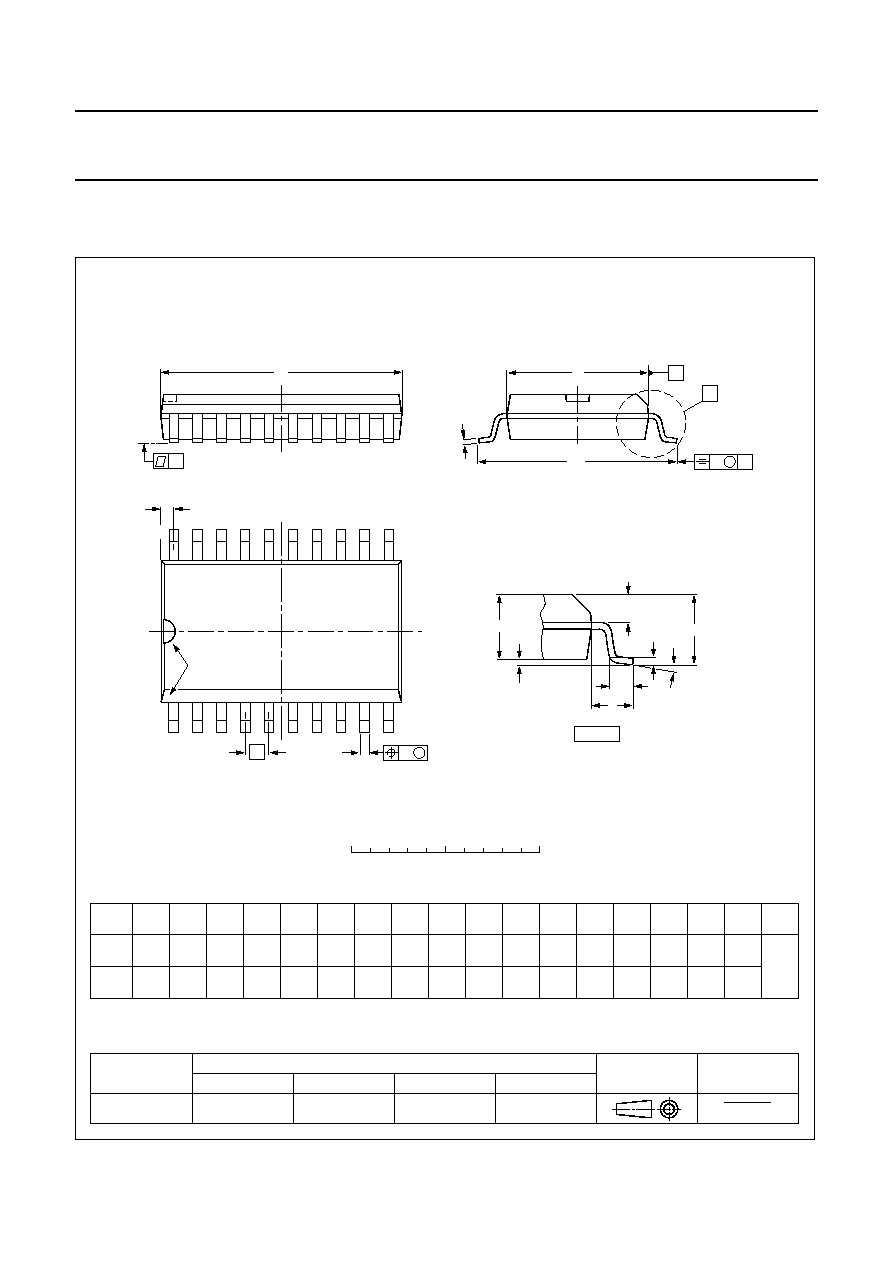
PACKAGE OUTLINE
UNIT
A
max.
A
1
A
2
A
3
b
p
c
D
(1)
E
(1)
(1)
e
H
E
L
L
p
Q
Z
y
w
v
REFERENCES
OUTLINE
VERSION
EUROPEAN
PROJECTION
ISSUE DATE
IEC
JEDEC
EIAJ
mm
inches
2.65
0.30
0.10
2.45
2.25
0.49
0.36
0.32
0.23
13.0
12.6
7.6
7.4
1.27
10.65
10.00
1.1
1.0
0.9
0.4
8
0
o
o
0.25
0.1
DIMENSIONS (inch dimensions are derived from the original mm dimensions)
Note
1. Plastic or metal protrusions of 0.15 mm maximum per side are not included.
1.1
0.4
SOT163-1
10
20
w
M
b
p
detail X
Z
e
11
1
D
y
0.25
075E04
MS-013AC
pin 1 index
0.10
0.012
0.004
0.096
0.089
0.019
0.014
0.013
0.009
0.51
0.49
0.30
0.29
0.050
1.4
0.055
0.419
0.394
0.043
0.039
0.035
0.016
0.01
0.25
0.01
0.004
0.043
0.016
0.01
0
5
10 mm
scale
X
A
A
1
A
2
H
E
L
p
Q
E
c
L
v
M
A
(A )
3
A
SO20: plastic small outline package; 20 leads; body width 7.5 mm
SOT163-1
95-01-24
97-05-22

January 1992
18
Philips Semiconductors
Preliminary specification
Sound fader control circuit
for car radios
TEA6330T
SOLDERING
Introduction
There is no soldering method that is ideal for all IC
packages. Wave soldering is often preferred when
through-hole and surface mounted components are mixed
on one printed-circuit board. However, wave soldering is
not always suitable for surface mounted ICs, or for
printed-circuits with high population densities. In these
situations reflow soldering is often used.
This text gives a very brief insight to a complex technology.
A more in-depth account of soldering ICs can be found in
our
"IC Package Databook" (order code 9398 652 90011).
Reflow soldering
Reflow soldering techniques are suitable for all SO
packages.
Reflow soldering requires solder paste (a suspension of
fine solder particles, flux and binding agent) to be applied
to the printed-circuit board by screen printing, stencilling or
pressure-syringe dispensing before package placement.
Several techniques exist for reflowing; for example,
thermal conduction by heated belt. Dwell times vary
between 50 and 300 seconds depending on heating
method. Typical reflow temperatures range from
215 to 250
∞
C.
Preheating is necessary to dry the paste and evaporate
the binding agent. Preheating duration: 45 minutes at
45
∞
C.
Wave soldering
Wave soldering techniques can be used for all SO
packages if the following conditions are observed:
∑
A double-wave (a turbulent wave with high upward
pressure followed by a smooth laminar wave) soldering
technique should be used.
∑
The longitudinal axis of the package footprint must be
parallel to the solder flow.
∑
The package footprint must incorporate solder thieves at
the downstream end.
During placement and before soldering, the package must
be fixed with a droplet of adhesive. The adhesive can be
applied by screen printing, pin transfer or syringe
dispensing. The package can be soldered after the
adhesive is cured.
Maximum permissible solder temperature is 260
∞
C, and
maximum duration of package immersion in solder is
10 seconds, if cooled to less than 150
∞
C within
6 seconds. Typical dwell time is 4 seconds at 250
∞
C.
A mildly-activated flux will eliminate the need for removal
of corrosive residues in most applications.
Repairing soldered joints
Fix the component by first soldering two diagonally-
opposite end leads. Use only a low voltage soldering iron
(less than 24 V) applied to the flat part of the lead. Contact
time must be limited to 10 seconds at up to 300
∞
C. When
using a dedicated tool, all other leads can be soldered in
one operation within 2 to 5 seconds between
270 and 320
∞
C.

January 1992
19
Philips Semiconductors
Preliminary specification
Sound fader control circuit
for car radios
TEA6330T
DEFINITIONS
LIFE SUPPORT APPLICATIONS
These products are not designed for use in life support appliances, devices, or systems where malfunction of these
products can reasonably be expected to result in personal injury. Philips customers using or selling these products for
use in such applications do so at their own risk and agree to fully indemnify Philips for any damages resulting from such
improper use or sale.
Data sheet status
Objective specification
This data sheet contains target or goal specifications for product development.
Preliminary specification
This data sheet contains preliminary data; supplementary data may be published later.
Product specification
This data sheet contains final product specifications.
Limiting values
Limiting values given are in accordance with the Absolute Maximum Rating System (IEC 134). Stress above one or
more of the limiting values may cause permanent damage to the device. These are stress ratings only and operation
of the device at these or at any other conditions above those given in the Characteristics sections of the specification
is not implied. Exposure to limiting values for extended periods may affect device reliability.
Application information
Where application information is given, it is advisory and does not form part of the specification.