
PLL207-151
Frequency Generator with 200MHz Differential CPU Clocks
47745 Fremont Blvd., Fremont, California 94538 TEL (510) 492-0990 FAX (510) 492-0991 Rev 11/27/02 Page 1
FEATURES
∑
Supports 3 pair of differential CPU clocks for
INTEL Brookdale chipsets.
∑
Programmable Spread Spectrum Modulation
from
±
0.1% to
±
1.5% with minimum step size of
±
0.012%. Selectable either center or down.
∑
Selectable Spread Spectrum modulation profile.
∑
AccuSkew
TM,
Programmable Precision skew
tuning channel with maximum
±
5% precision
over the variation of temperature, process and
voltage. Finest step starts with 80ps.
∑
AccuDrive
TM
Programmable Output Buffer drive
strength with minimum 6mA per step.
∑
7 PCI, 3 PCI_F, 1 USB, 1 DOT, 1 REF, 5 3V66
∑
One 3V66/VCH (3.3V) at 66.66MHz or 48MHz.
∑
Power management control to stop CPU, PCI.
∑
Support 2-wire I2C serial bus interface.
∑
Single byte micro-step linear Frequency
programming via I2C with smooth switching.
∑
Available in 300 mil 56 pin SSOP.
BLOCK DIAGRAM
PIN CONFIGURATION
Note:
^
:
Pull up (100k
),
#: Active low,
*
: Bi-directional latched at power-up
POWER GROUP
∑
VDD1, VSS1: REF, XIN, XOUT, PLL ANALOG
∑
VDD2, VSS2: PCI
∑
VDD3, VSS3: 3V66
∑
VDD4, VSS4: 48MHz
∑
VDD5, VSS5: CPUT & CPUC
KEY SPECIFICATIONS
∑
CPU Output Jitter < 200ps
∑
3V66 Output Jitter < 250ps
∑
CPU Output Skew < 150 ps
XIN
SDATA
SCLK
FS (0:2)*
XTAL
OSC
I2C
Logic
PLL1
SST
Control
Logic
REF
CPUT0
XOUT
CPUC0
CPUT1
CPUC1
CPUT2
CPUC2
CPU_STOP#
PD#
PCI(0:6)
PCI_F(0:2)
3V66 (1:5)
I
REF
PLL
2
48MHz_USB
48MHz_DOT
3V66_0/VCH
MULTSEL0
PCI_STOP#
PLL207-151
VSS3
VDD3
PCI6
PCI5
PCI4
VSS2
PCI_F1
PCI_F0
VSS1
XOUT
XIN
VDD1
PD#/^
3V66_2
PCI0
CPUT1
CPUC1
VSS5
VDD5
CPUT2
CPUC2
MULTSEL0^
I
REF
VSS_I
REF
FS2
48MHz_USB
REF
CPU_STOP#^
CPUT0
CPUC0
VDD5
48MHz_DOT
3V66_0/VCH
VDD4
VSS4
PCI_STOP#^
SDATA
SCLK
VSS3
VDD3
3V66_1
1
2
3
4
5
6
7
8
9
10
11
12
13
14
15
16
17
18
19
20
21
22
23
24
28
27
26
25
48
47
46
45
44
43
42
41
40
39
38
37
36
35
34
33
32
31
30
29
49
50
52
51
53
54
55
56
PCI_F2
VDD2
VSS2
PCI1
PCI2
PCI3
VDD2
3V66_3
3V66_4
3V66_5
VDD1
VSS1
Vtt_PWRGD#
FS1
FS0

PLL207-151
Frequency Generator with 200MHz Differential CPU Clocks
47745 Fremont Blvd., Fremont, California 94538 TEL (510) 492-0990 FAX (510) 492-0991 Rev 11/27/02 Page 2
PIN DESCRIPTIONS
Name
Number
Type
Description
VDD
1,8,14,19,26,
32,37,46,50
P
3.3V Power Supply.
XIN
2
I
14.318Mhz crystal input to be connected to one end of the crystal.
XOUT
3
O
14.318Mhz crystal output.
PCI_F(0:2)
5,6,7
O
PCI clock optionally not affected by PCI_STOP (see I2C Byte 3). PCI_F will
all be left free running if I2C Byte 3 bit [3:5] = 0, but will be stopped if I2C
Byte 3 bit [3:5] = 1. They have 20 ohms on-chip series resistor.
PCI(0:6)
10,11,12,13,
16,17,18
O
PCI clock outputs. They have 20 ohms on-chip series resistor.
3V66(1:5)
21,22,23,24,
33
O
66MHz reference clock from internal VCO. It has a 20 ohms on-chip series
resistor.
PD#
25
I
Power Down Control input. When low, Power Down will disable all clock
outputs including internal VCO and crystal clock. This pin has a 100k
internal pull-up.
Vtt_PWRGD#
28
I
This 3.3V LVTTL input is a level sensitive strobe used to determine when FS
(0:2) and MULTSEL0 inputs are valid and ready to be sampled (active low).
SDATA
29
B
SCLK
30
I
Serial data inputs for serial interface port.
PCI_STOP#
34
I
Halts PCI clocks when low (except PCI_F which are free running). This pin
has a 100k
internal pull-up.
3V66_0/VCH
35
O
3.3V output selectable through I2C to be 66MHz from internal VCO or 48MHz
(non-Speed Spectrum Controlled). It has a 20 ohms on-chip series resistor.
48MHz_DOT
38
O
48MHz output for DOT. It has a 20 ohms on-chip series resistor.
48MHz_USB
39
O
48MHz output for USB. It has a 20 ohms on-chip series resistor.
FS2
40
I
Frequency select pins.
I
REF
42
O
This pin establishes the reference current for the CPU pairs, it requires a
fixed precision resistor tied to ground in order to establish the appropriate
current.
MULTSEL0
43
I
This input is selecting the current multiplier for CPU outputs. This pin has a
100k
internal pull-up.
CPUC(0:2)
44,48,51
O
Complementary clock of differential pair of CPU outputs.
CPUT(0:2)
45,49,52
O
True clock of differential pair of CPU outputs.
CPU_STOP
53
I
Halts CPU clocks when input low. This pin has a 100k
internal pull-up.

PLL207-151
Frequency Generator with 200MHz Differential CPU Clocks
47745 Fremont Blvd., Fremont, California 94538 TEL (510) 492-0990 FAX (510) 492-0991 Rev 11/27/02 Page 3
PIN DESCRIPTIONS (CONTINUED)
Name
Number
Type
Description
FS(0:1)
54,55
I
Frequency select pins.
REF
56
O
14.318MHz reference clock. It has a 20 ohms on-chip series resistor.
VSS_I
REF
41
P
Current reference programming input for CPU buffers. This pin is returned to
device VSS.
VSS
4,9,15,20,27,
31,36,47
P
0.0V Power Supply.
FEQUENCY (MHz) SELECTION TABLE
FS2
FS1
FS0
CPU
3V66
PCI_F, PCI
Spread Spectrum
modulation rate
0
0
0
66.66
66.66
33.3
0 to ≠0.5% down spread
0
0
1
100
66.66
33.3
0 to ≠0.5% down spread
0
1
0
200
66.66
33.3
0 to ≠0.5% down spread
0
1
1
133.3
66.66
33.3
0 to ≠0.5% down spread
1
0
0
66.66
66.66
33.3
0 to ≠0.75% down spread
1
0
1
100
66.66
33.3
0 to ≠0.75% down spread
1
1
0
200
66.66
33.3
0 to ≠0.75% down spread
1
1
1
133.3
66.66
33.3
0 to ≠0.75% down spread
Mid
0
0
Tristate
Tristate
Tristate
N/A
Mid
0
1
TCLK/2
TCLK/4
TCLK/8
N/A
Mid
1
0
Reserved
Reserved
Reserved
N/A
Mid
1
1
Reserved
Reserved
Reserved
N/A
POWER MANAGEMENT CONIGURATION
PD# CPU_STOP# PCI_STOP# CPUT CPUC 3V66 PCI_F
PCI
USB/DOT PLL/OSC
0
X
X
IREF*2 FLOAT
LOW
LOW
LOW
LOW
OFF
1
0
0
IREF*2 FLOAT
ON
ON
ON
ON
ON
1
0
1
IREF*2 FLOAT
ON
ON
ON
ON
ON
1
1
0
ON
ON
ON
ON
ON
ON
ON
1
1
1
ON
ON
ON
ON
ON
ON
ON

PLL207-151
Frequency Generator with 200MHz Differential CPU Clocks
47745 Fremont Blvd., Fremont, California 94538 TEL (510) 492-0990 FAX (510) 492-0991 Rev 11/27/02 Page 4
HOST SWING SELECT FUNCTIONS
MULT_SEL0 Board target trace (Z) Reference R (Rr); IREF = VDD/(3*Rr) Output Current Voh @ Z
0
50
Rr = 221
(1%); IREF = 5.00mA
Ioh = 4 x IREF
1.0V @
50
1
50
Rr = 475
(1%); IREF = 2.32mA
Ioh = 6 x IREF
0.7V @
50
MAXIMUM ALLOWED CURRENT
Conditions
Max. 3.3 supply consumption
VDD = 3.465V All static inputs = VDD or GND
Powerdown Mode (PD# = 0)
25mA @ Iref = 2.32 mA, 45mA @ Iref = 5.0mA
Full Active
280 mA
TIMING DIAGRAMS & PHASE RELATIONSHIP
Figure:
3V66 & PCI Phase Relationship ( Un-Buffered Mode )
Group Skews at Common Transition Edges: ( Un-Buffered Mode)
Group
Symbols
Description
Min
Max
Units
3V66
3V66
3V66(0:5) pin-to-pin skew
0
500
ps
PCI
PCI
PCI_F(0:2) and PCI (0:6)
pin-to-pin skew
0
500
ps
3V66 to PCI
T PCI
3V66(0:5) leads 33MHz PCI
1.5
3.5
ns
3V66(0:1)
3V66(2:4)
3V66_5
PCI_F(0:2) / PCI(0:6)
T
pci
PLL207-151
Frequency Generator with 200MHz Differential CPU Clocks
47745 Fremont Blvd., Fremont, California 94538 TEL (510) 492-0990 FAX (510) 492-0991 Rev 11/27/02 Page 5
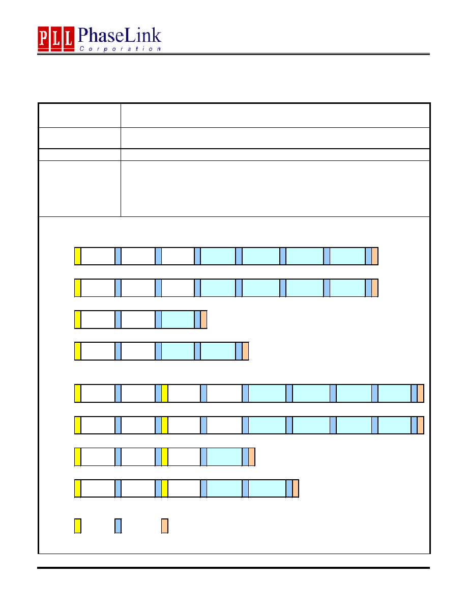
I2C BUS CONFIGURATION SETTING
Address Assignment
A6 A5 A4 A3 A2 A1 A0 R/W
1 1 0 1 0 0 1 _
Slave
Receiver/Transmitter Provides both slave write and read back functionality
Data Transfer Rate
Standard mode at 100kbits/s
Data Protocol
This serial interface is designed to allow multiple protocols to write and read from the
controller. It includes Block Read/Write, Block Index Read/Write, Byte Read/Write and Word
Read/Write. In general, the bytes must be accessed in sequential order from lowest to highest
byte. Each byte transferred must be followed by 1 acknowledge bit. A byte transferred without
acknowledged bit will terminate the transfer. The write or read block both begins with the
master sending a slave address and a write condition (0xD2) or a read condition (0xD3).
WRITE MODE
Block
Write
S
Address
D2
A
Command
00
A
A
A
A
A
A P
Block
Index Write
S
Address
D2
A
Command M
=(00~22)
A
A
A
A
A
A P
Byte Write
S
Address
D2
A
Command M'
=(00~22)+128
A
A P
Word Write
S
Address
D2
A
Command M'
=(00~22)+128
A
A
A P
READ MODE
Block
Read
S
Address
D2
A
Command
00
A S
A
A
A
A
A
Data
Byte N
A P
Block
Index Read
S
Address
D2
A
Command M
=(00~22)
A S
A
A
A
A
A
Data
Byte M+N-1
A P
Byte Read
S
Address
D2
A
Command M'
=(00~22)+128
A S
A
A P
Word Read
S
Address
D2
A
Command M'
=(00~22)+128
A S
A
A
A P
Legend:
S Start
A
P Stop
Data
Byte M
Address
D3
Byte count
N
Data
--------
Data
Byte M+1
Data
Byte M
Data
Byte N
Byte count
N
Data
Byte M
Data
Byte M+1
Data
--------
Data
Byte M+N-1
Data
Byte 2
Data
--------
Byte count
N
Data
Byte 1
Address
D3
Byte count
N
Data
Byte 1
Data
Byte 2
Data
Byte M+1
Data
--------
Address
D3
Data
Byte M
Data
Byte M
Acknowledge to
host
Address
D3
Data
Byte M
Data
Byte M+1