 | ÐлекÑÑоннÑй компоненÑ: PLL701-15 | СкаÑаÑÑ:  PDF PDF  ZIP ZIP |
FEATURES
Preliminary
PLL701-15
Low EMI Spread Spectrum Multiplier Clock
FEATURES
· Spread Spectrum clock with frequency range of
33 ~ 90MHz.
· Output frequency 1X the input frequency.
· Less than 250 ps skew between outputs.
· Less than 100 ps cycle - cycle jitter.
· ±0.50% Center Spread Modulation.
· TTL/CMOS compatible outputs.
· 3.3V operation.
· Available in 8-Pin 150mil SOIC.
DESCRIPTIONS
The PLL701-15 is a Spread Spectrum Clock
Generator designed for the purpose of reducing EMI
in high-speed digital systems. The device is designed
to operate from 33 ~ 90MHz and provides five low-
skew outputs.
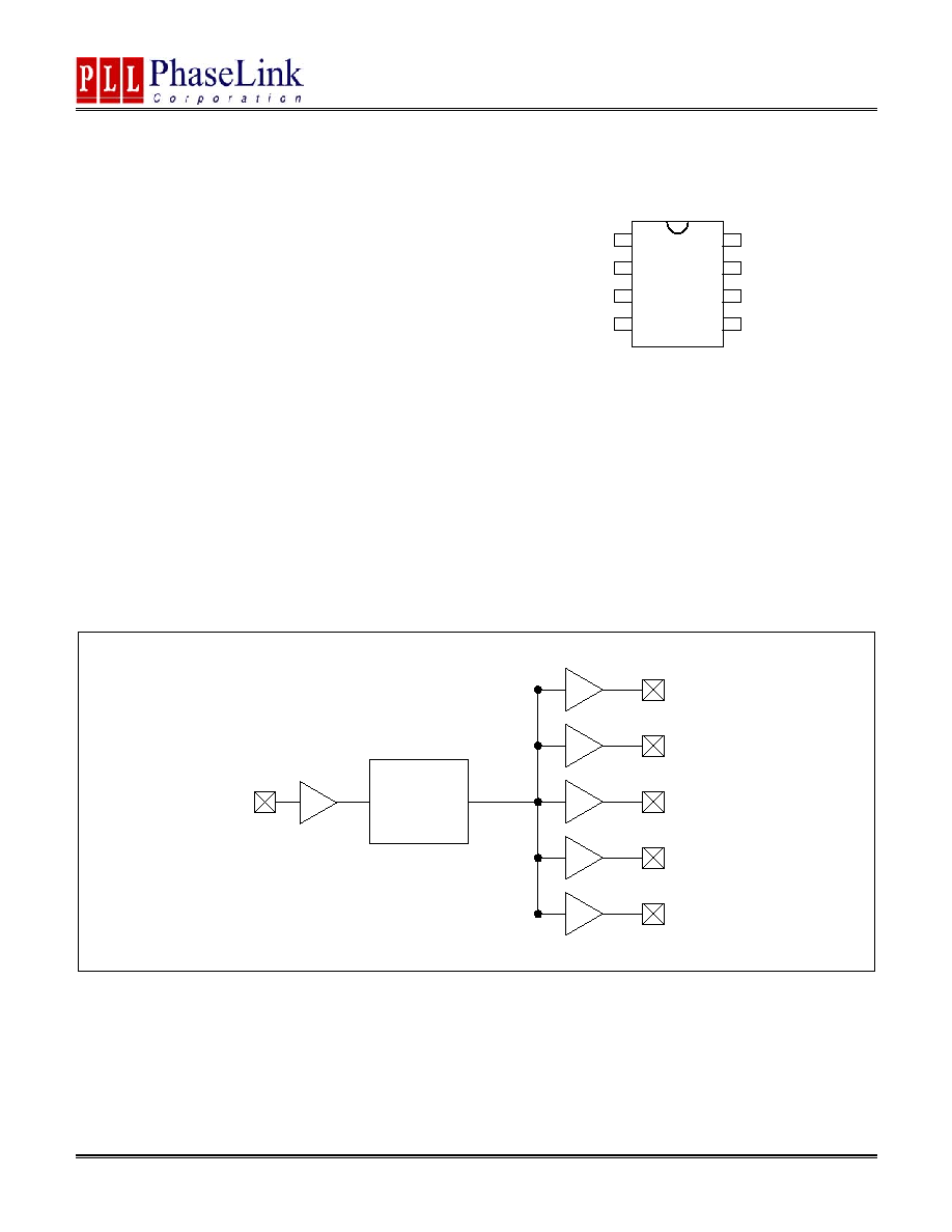
PIN CONFIGURATION
PLL701-15
1
2
3
4
5
6
7
8
FIN
CLK2
CLK1
GND
CLK5
VDD
CLK3
CLK4
FIN = 33 ~ 90 Mhz
BLOCK DIAGRAM
PLL SST
1X
FIN
CLK1
CLK2
CLK3
CLK4
CLK5
47745 Fremont Blvd., Fremont, California 94538 TEL (510) 492-0990 FAX (510) 492-0991 Rev 2/24/03 Page 1
Preliminary
PLL701-15
Low EMI Spread Spectrum Multiplier Clock
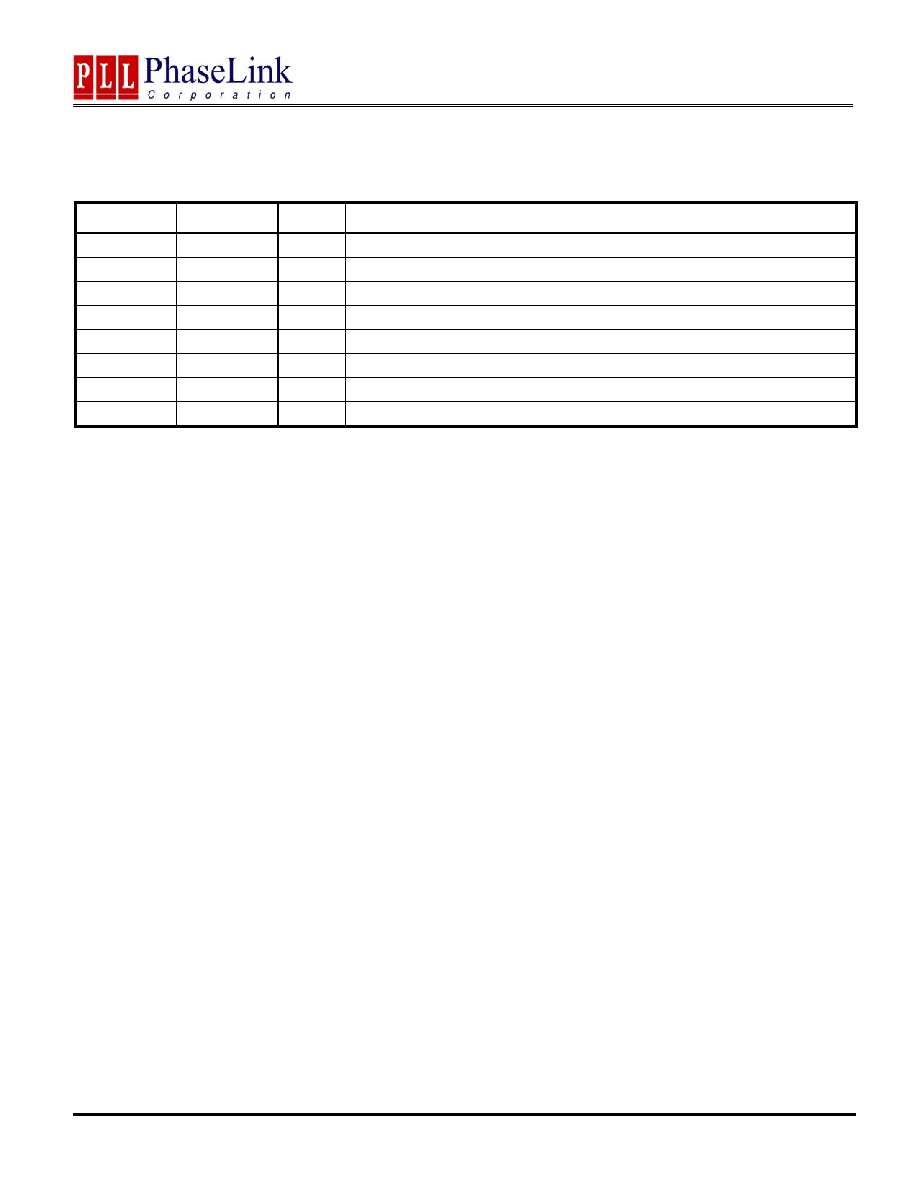
PIN DESCRIPTIONS
Name Number
Type
Description
FIN
1
I
Input Clock Frequency. ( 33 ~ 90MHz )
CLK2
2
O
Buffered Clock Output. 1X the input frequency ( FIN ).
CLK1
3
O
Buffered Clock Output. 1X the input frequency ( FIN ).
GND 4 I
Ground.
CLK3
5
O
Buffered Clock Output. 1X the input frequency ( FIN ).
VDD
6
P
3.3V Power Supply.
CLK4
7
O
Buffered Clock Output. 1X the input frequency ( FIN ).
CLK5
8
O
Buffered Clock Output. 1X the input frequency ( FIN ).
47745 Fremont Blvd., Fremont, California 94538 TEL (510) 492-0990 FAX (510) 492-0991 Rev 2/24/03 Page 2
Preliminary
PLL701-15
Low EMI Spread Spectrum Multiplier Clock
ELECTRICAL SPECIFICATIONS
1. Absolute Maximum Ratings
PARAMETERS SYMBOL
MIN.
MAX.
UNITS
Supply Voltage Range
V
CC
-
0.5
7 V
Input Voltage Range
V
I
-
0.5 V
CC
+
0.5
V
Output Voltage Range
V
O
-
0.5 V
CC
+
0.5
V
Soldering Temperature
260
°C
Storage Temperature
T
S
-65 150
°C
Ambient Operating Temperature*
T
A
-40 85
°C
ESD Voltage
2
kV
Exposure of the device under conditions beyond the limits specified by Maximum Ratings for extended periods may cause permanent damage to the
device and affect product reliability. These conditions represent a stress rating only, and functional operations of the device at these or any other
conditions above the operational limits noted in this specification is not implied
* Note: Operating Temperature is guaranteed by design for all parts (COMMERCIAL and INDUSTRIAL), but tested for INDUSTRIAL grade only.
2. Electrical Characteristics
V
DD
= 3.0~3.6V, unless otherwise stated
PARAMETERS SYMBOL CONDITIONS
MIN.
TYP.
MAX.
UNITS
Input Low Voltage
V
IL
0.8
V
Input High Voltage
V
IH
2.0
V
Input Low Current
I
IL
V
IN
= 0V
19
50.0
µA
Input High Current
I
IH
V
IN
= V
DD
0.10
100.0
µA
Output Low Voltage
V
OL
I
OL
= 50 mA
0.25
0.4
V
Output High Voltage
V
OH
I
OH
= 50 mA
2.4
2.9
V
Supply Current
I
DD
Unloaded outputs at 75MHz,
SEL inputs at V
DD
or GND
30.0
40.0
mA
47745 Fremont Blvd., Fremont, California 94538 TEL (510) 492-0990 FAX (510) 492-0991 Rev 2/24/03 Page 3
Preliminary
PLL701-15
Low EMI Spread Spectrum Multiplier Clock
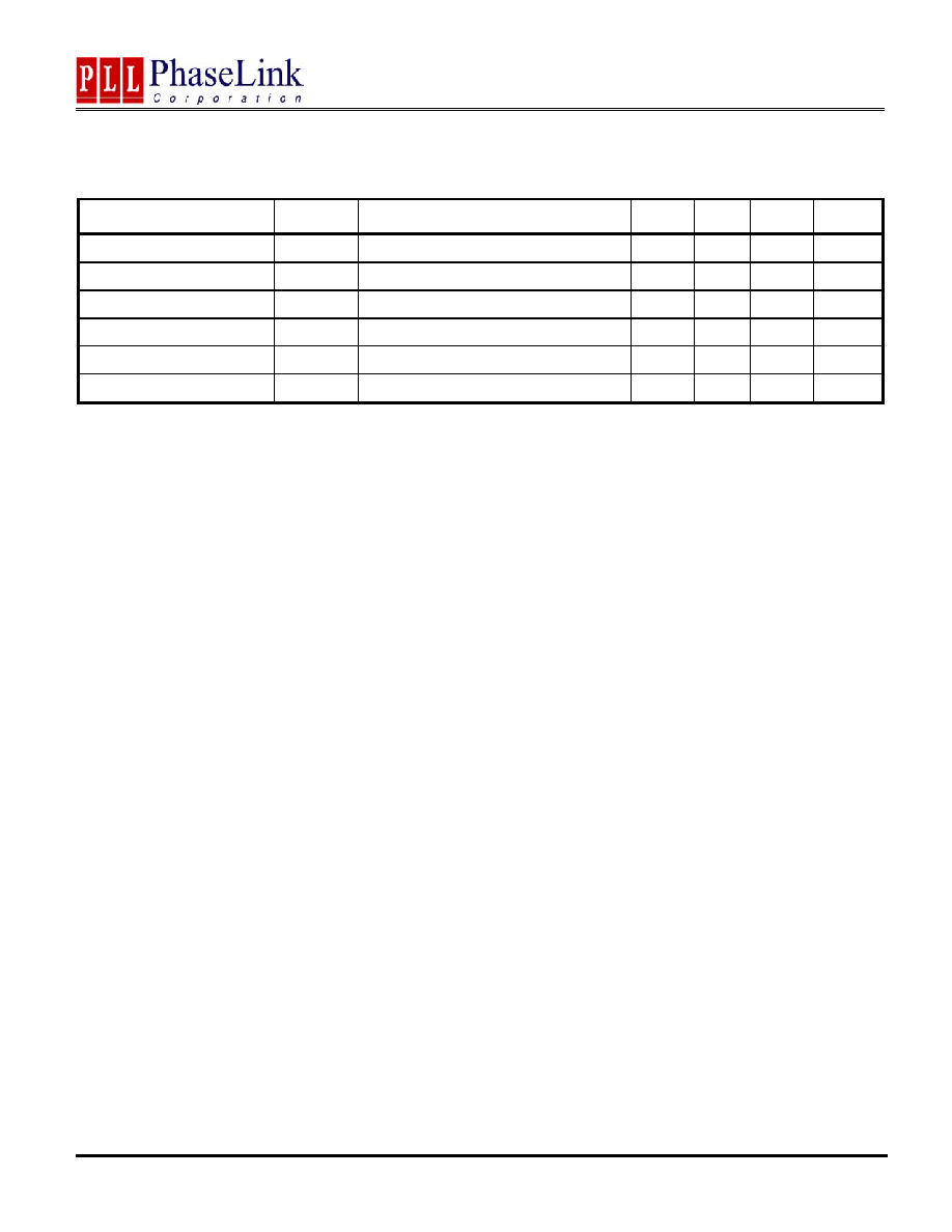
3. TIMING CHARACTERISTICS
PARAMETERS SYMBOL
CONDITIONS
MIN.
TYP.
MAX.
UNITS
Input Frequency
F
IN
33
90
MHz
Rise Time
T
r
Measured at 0.8V ~ 2.0V @ 3.3V
0.8
0.95
1.1
ns
Fall Time
T
f
Measured at 2.0V ~ 0.8V @ 3.3V
0.78
0.85
0.9
ns
Output Duty Cycle
D
T
45
50
55
%
Input to Output Delay
2
4
ns
Cycle to Cycle Jitter
T
cyc-cyc
Over output frequency range @ 3.3V
100
ps
47745 Fremont Blvd., Fremont, California 94538 TEL (510) 492-0990 FAX (510) 492-0991 Rev 2/24/03 Page 4
Preliminary
PLL701-15
Low EMI Spread Spectrum Multiplier Clock
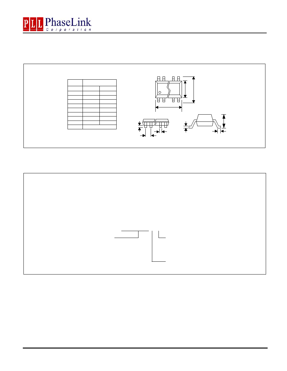
PACKAGE INFORMATION
C
L
A
8 PIN Narrow SOIC ( mm )
SOIC
Symbol
Min.
Max.
A
1.47
1.73
A1
0.10
0.25
B
0.33
0.51
C
0.19
0.25
D
4.80
4.95
E
3.80
4.00
H
5.80
6.20
L
0.38
1.27
e
1.27 BSC
E
H
D
A1
e
B
ORDERING INFORMATION
For part ordering, please contact our Sales Department:
47745 Fremont Blvd., Fremont, CA 94538, USA
Tel: (510) 492-0990 Fax: (510) 492-0991
PART NUMBER
The order number for this device is a combination of the following:
Device number, Package type and Operating temperature range
PLL701-15 S C
TEMPERATURATURE
C=COMMERCIAL
M=MILITARY
I=INDUSTRAL
PACKAGE TYPE
S=SOIC
PART NUMBER
PhaseLink Corporation, reserves the right to make changes in its products or specifications, or both at any time without notice. The information
furnished by Phaselink is believed to be accurate and reliable. However, PhaseLink makes no guarantee or warranty concerning the accuracy of said
information and shall not be responsible for any loss or damage of whatever nature resulting from the use of, or reliance upon this product.
LIFE SUPPORT POLICY: PhaseLink's products are not authorized for use as critical components in life support devices or systems without the
express written approval of the President of PhaseLink Corporation.
47745 Fremont Blvd., Fremont, California 94538 TEL (510) 492-0990 FAX (510) 492-0991 Rev 2/24/03 Page 5