TISP61CAP3
PROGRAMMABLE
OVERVOLTAGE PROTECTOR
P R O D U C T I N F O R M A T I O N
1
SEPTEMBER 1994 - REVISED SEPTEMBER 1997
Copyright © 1997, Power Innovations Limited, UK
Information is current as of publication date. Products conform to specifications in accordance
with the terms of Power Innovations standard warranty. Production processing does not
necessarily include testing of all parameters.
PROGRAMMABLE SLIC OVERVOLTAGE PROTECTION
q
Programmable Voltage Triggered SCR
with high Holding Current
q
Transistor Buffered Inputs for Low V
GG
current
q
Rated for International Surge Wave Shapes
description
The TISP61CAP3 is a programmable
overvoltage protector designed to protect SLIC
applications against lightning and transients
induced by ac power lines. Normally the V
GG
(Gate) terminal will be connected to the negative
supply rail of the SLIC
When a negative transient exceeds the negative
supply rail voltage of the SLIC it will cause the
thyristor to crowbar, shunting the surge to
ground. The high crowbar holding current
prevents dc latchup as the transient subsides.
Positive transients are clipped by diode action.
WAVE SHAPE
STANDARD
I
TSP
A
10/700 µs
CCITT IX K17
38
10/1000 µs
REA PE-60
30
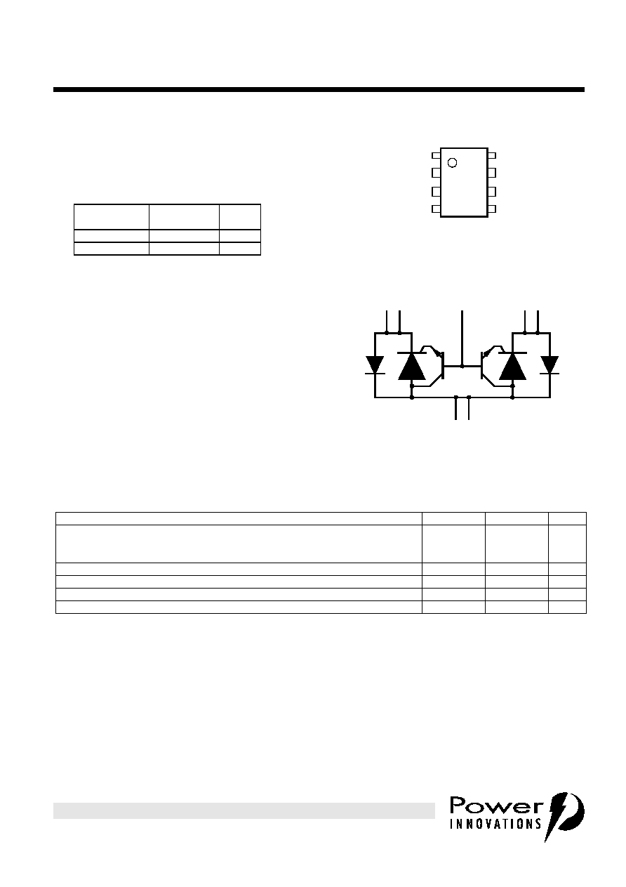
device symbol
Terminals K1, K2 and A correspond to the alternative
line designators of T, R and G or A, B and C. The
negative protection voltage is controlled by the voltage,
V
GG,
applied to the G terminal.
SD6XAE
A
K1
G
K2
MD6XAV
P PACKAGE
(TOP VIEW)
NC - No internal connection
Terminal typical application names shown in
parenthesis
1
2
3
4
5
6
7
8
K2
G
K1
NC
K1
A
A
K2
(Tip)
(Ground)
(Ground)
(Ring)
(Gate)
(Tip)
(Ring)
absolute maximum ratings
NOTES: 1. Above 70∞C, derate linearly to zero at 150∞C case temperature
2. This value applies when the initial case temperature is at (or below) 70∞C. The surge may be repeated after the device has
returned to thermal equilibrium.
3. Most PTT's quote an unloaded voltage waveform. In operation the TISP essentially shorts the generator output. The resulting
loaded current waveform is specified.
RATING
SYMBOL
VALUE
UNIT
Non-repetitive peak on-state pulse current (see Notes 1, 2 and 3)
I
TSP
A
5/310 µs (CCITT IX K17, open-circuit voltage wave shape 1.5 kV, 10/700 µs)
38
10/1000 µs (REA PE-60, open-circuit voltage wave shape 10/1000 µs)
30
Non-repetitive peak on-state current, 50 Hz, 1 s (see Notes 1 and 2)
I
TSM
2.5
A rms
Maximum gate current
I
GM
2
A
Repetitive peak off-state voltage
V
DRM
- 80
V
Maximum gate supply voltage
V
GG(max)
- 80
V

TISP61CAP3
PROGRAMMABLE
OVERVOLTAGE PROTECTOR
2
SEPTEMBER 1994 - REVISED SEPTEMBER 1997
P R O D U C T I N F O R M A T I O N
NOTE
4: These capacitance measurements employ a three terminal capacitance bridge incorporating a guard circuit. The third terminal is
connected to the guard terminal of the bridge.
electrical characteristics, T
J
= 25∞C
PARAMETER
TEST CONDITIONS
MIN
TYP
MAX
UNIT
V
F
Forward voltage
I
F
= 5 A
3
V
V
FR
Forward recovery
voltage
dv/dt = 300 V/
µ
s
di/dt < 10 A/
µ
s
R
SOURCE
= 30
7
V
V
GK(BO)
Gate cathode voltage
at breakover
(V
(BO)
- V
GG
)
dv/dt = -250 V/ms
-72 < V
GG
< -10 V
R
SOURCE
= 300
-3
V
V
GK(BO)
Impulse gate cathode
voltage at breakover
(V
(BO)
- V
GG
)
dv/dt = -300 V/
µ
s
di/dt < -10 A/
µ
s
-72 < V
GG
< -10 V
R
SOURCE
= 30
-15
V
V
T
On-state voltage
I
T
= -4 A
-72 < V
GG
< -10 V
-3
V
I
D
Off-state current
V
D
= -80 V
V
GG
= -80 V
-10
µ
A
I
S
Switching current
dv/dt = -250 V/ms
-72 < V
GG
< -10 V
R
SOURCE
= 300
-0.15
A
I
H
Holding current
di/dt = 30 mA/
µ
s
-72 < V
GG
< -10 V
-0.15
A
I
GAO
Gate reverse current
with cathode open
V
GG
= -72 V
-10
µ
A
I
GAT
Gate reverse current
in the on-state
V
GG
= -72 V
I
T
= -0.5 A
-1
mA
I
GAF
Gate reverse current
in the forward
conducting state
V
GG
= -72 V
I
T
= 1 A
I
T
= 5 A
-10
-30
mA
I
GSM
Peak gate switching
current
dv/dt = -250 V/ms
-72 < V
GG
< -10 V
R
SOURCE
= 300
5
mA
C
off
Off-state capacitance
-72 < V
GG
< -10 V
V
D
= -3 V
V
D
= -48 V
(see Note 4)
150
80
pF
dv/dt
Critical rate of rise of
off-state voltage
V
GG
= -72 V, linear ramp, Maximum ramp value > 0.85 V
GG
-50
V/
µ
s
3
SEPTEMBER 1994 - REVISED SEPTEMBER 1997
TISP61CAP3
PROGRAMMABLE
OVERVOLTAGE PROTECTOR
P R O D U C T I N F O R M A T I O N
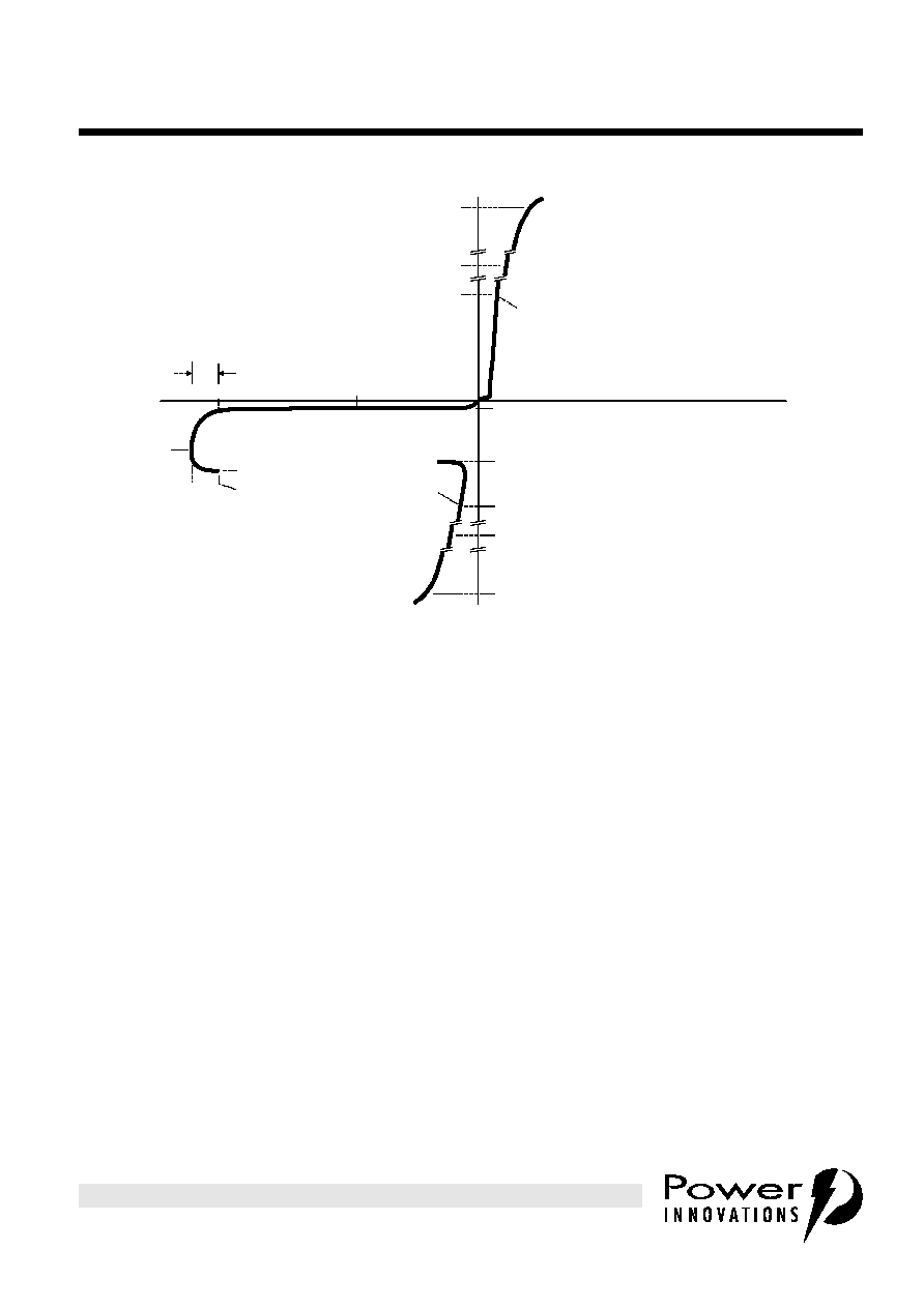
PARAMETER MEASUREMENT INFORMATION
Figure 1. VOLTAGE-CURRENT CHARACTERISTIC
-v
I
S
V
S
V
GG
V
D
I
H
I
T
V
T
I
TSM
I
TSP
V
(BO)
I
(BO)
I
D
Quadrant I
Forward
Conduction
Characteristic
+v
+i
I
F
V
F
I
TSM
I
TSP
-i
Quadrant III
Switching
Characteristic
PM6XAA
V
GK(BO)
TISP61CAP3
PROGRAMMABLE
OVERVOLTAGE PROTECTOR
4
SEPTEMBER 1994 - REVISED SEPTEMBER 1997
P R O D U C T I N F O R M A T I O N
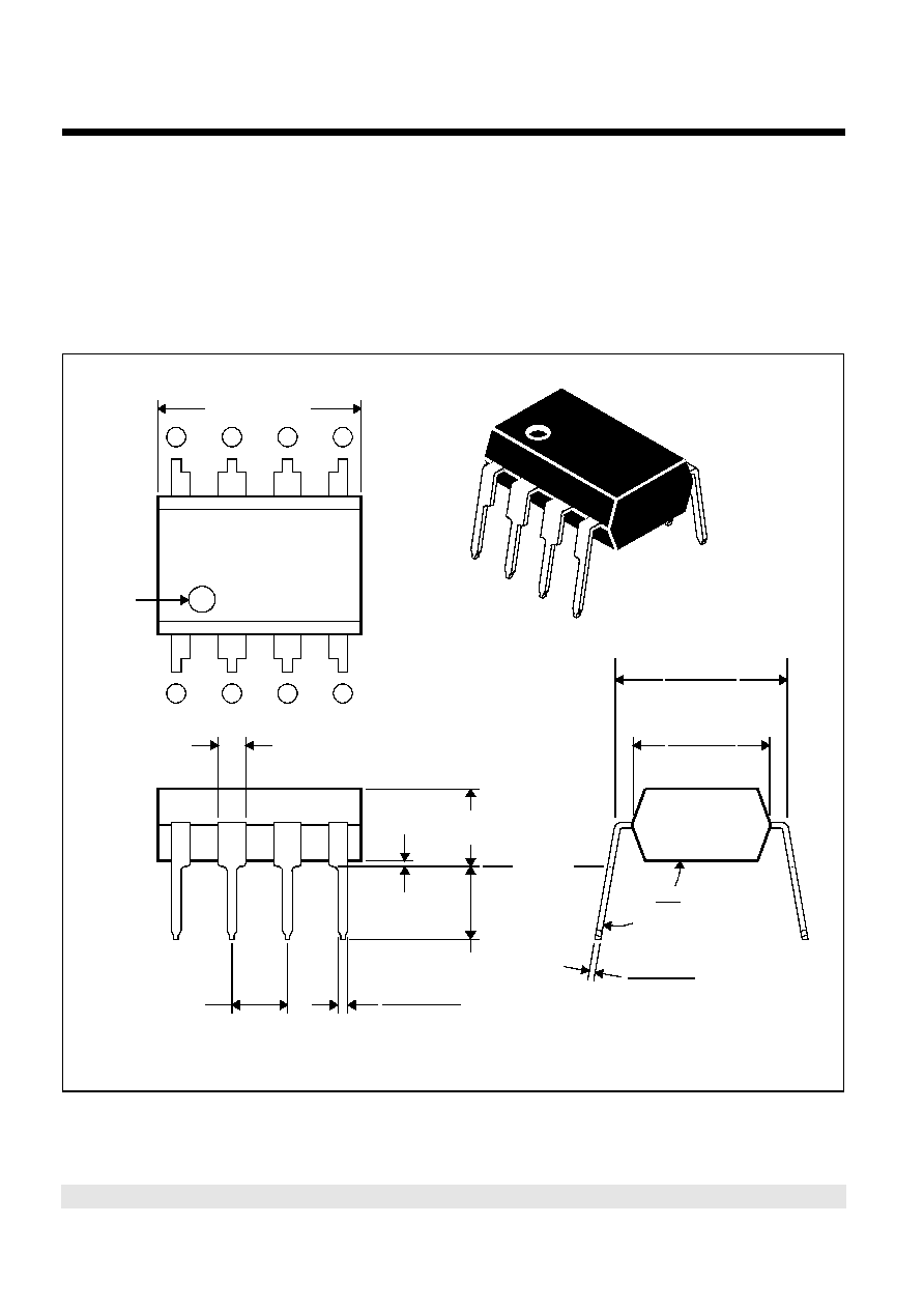
P008
plastic dual-in-line package
This dual-in-line package consists of a circuit mounted on a lead frame and encapsulated within a plastic
compound. The compound will withstand soldering temperature with no deformation, and circuit performance
characteristics will remain stable when operated in high humidity conditions The package is intended for
insertion in mounting-hole rows on 7,62 (0.300) centers. Once the leads are compressed and inserted,
sufficient tension is provided to secure the package in the board during soldering. Leads require no
additional cleaning or processing when used in soldered assembly.
MECHANICAL DATA
1
2
3
4
8
7
6
5
10,2 (0.400) MAX
Index
Dot
1,78 (0.070) MAX
4 Places
5,08 (0.200)
MAX
0,51 (0.020)
MIN
2,54 (0.100) T.P.
6 Places
(see Note A)
0,533 (0.021)
0,381 (0.015)
8 Places
3,17 (0.125)
MIN
Seating
Plane
0,36 (0.014)
0,20 (0.008)
8 Places
105∞
90∞
8 Places
6,60 (0.260)
6,10 (0.240)
7,87 (0.310)
7,37 (0.290)
T.P.
C
L
C
L
ALL LINEAR DIMENSIONS ARE IN MILLIMETERS AND PARENTHETICALLY IN INCHES
P008
Designation per JEDEC Std 30:
PDIP-T8
NOTE A: Each pin centerline is located within 0,25 (0.010) of its true longitudinal position
MDXXABA

5
SEPTEMBER 1994 - REVISED SEPTEMBER 1997
TISP61CAP3
PROGRAMMABLE
OVERVOLTAGE PROTECTOR
P R O D U C T I N F O R M A T I O N
IMPORTANT NOTICE
Power Innovations Limited (PI) reserves the right to make changes to its products or to discontinue any
semiconductor product or service without notice, and advises its customers to verify, before placing orders, that the
information being relied on is current.
PI warrants performance of its semiconductor products to the specifications applicable at the time of sale in
accordance with PI's standard warranty. Testing and other quality control techniques are utilized to the extent PI
deems necessary to support this warranty. Specific testing of all parameters of each device is not necessarily
performed, except as mandated by government requirements.
PI accepts no liability for applications assistance, customer product design, software performance, or infringement
of patents or services described herein. Nor is any license, either express or implied, granted under any patent
right, copyright, design right, or other intellectual property right of PI covering or relating to any combination,
machine, or process in which such semiconductor products or services might be or are used.
PI SEMICONDUCTOR PRODUCTS ARE NOT DESIGNED, INTENDED, AUTHORIZED, OR WARRANTED TO BE
SUITABLE FOR USE IN LIFE-SUPPORT APPLICATIONS, DEVICES OR SYSTEMS.
Copyright © 1997, Power Innovations Limited