Document Outline
- FEATURES
- Package
- APPLICATION
- FUNCTION
- PART NAME TABLE
- PIN CONFIGURATION(TOP VIEW)
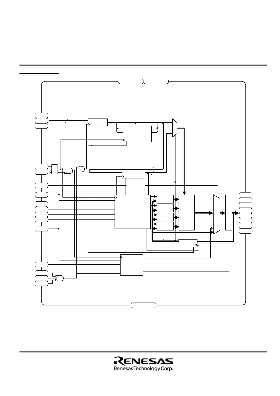
- BLOCK DIAGRAM
- PIN FUNCTION
- Read Operations
- Write Operation
- DC OPERATED TRUTH TABLE
- BURST SEQUENCE TABLE
- TRUTH TABLE
- STATE DIAGRAM
- WRITE TRUTH TABLE
- ABSOLUTE MAXIMUM RATINGS
- CAPACITANCE
- THERMAL RESISTANCE
- DC ELECTRICAL CHARACTERISTICS
- AC ELECTRICAL CHARACTERISTICS
- PACKAGE OUTLINE
Renesas LSIs
M5M5V5A36GP-75,85
18874368-BIT(524288-WORD BY 36-BIT) Flow-Through NETWORK SRAM
1/19
Preliminary
M5M5V5A36GP-75,85 REV.1.0
FEATURES
∑ Flow-Through Read mode, Single Late Write mode
∑ Fast access time: 7.5 ns and 8.5 ns
∑ Single 3.3V -5% and +5% power supply V
DD
∑ Separate V
DDQ
for 3.3V or 2.5V I/O
∑ Individual byte write (BWa# - BWd#) controls may be tied
LOW
∑ Single Read/Write control pin (W#)
∑ CKE# pin to enable clock and suspend operations
∑ Internally self-timed, registers outputs eliminate the need
to control G#
∑ Snooze mode (ZZ) for power down
∑ Three chip enables for simple depth expansion
Package
100pin TQFP
APPLICATION
High-end networking products that require high bandwidth, such
as switches and routers
.
FUNCTION
Synchronous circuitry allows for precise cycle control
triggered by a positive edge clock transition.
Synchronous signals include : all Addresses, all Data Inputs,
all Chip Enables (E1#, E2, E3#), Address Advance/Load (ADV),
Clock Enable (CKE#), Byte Write Enables (BWa#, BWb#, BWc#,
BWd#) and Read/Write (W#).
Write operations are controlled by the four Byte Write Enables
(BWa# - BWd#) and Read/Write(W#) inputs. All writes are
conducted with on-chip synchronous self-timed write circuitry.
Asynchronous inputs include Output Enable (G#), Clock (CLK)
and Snooze Enable (ZZ).
The HIGH input of ZZ pin puts the SRAM in the power-down
state.
All read, write and deselect cycles are initiated by the ADV
LOW input. Subsequent burst address can be internally
generated as controlled by the ADV HIGH input.
PART NAME TABLE
Part Name
Access
Cycle
Active Current
(max.)
Standby Current
(max.)
M5M5V5A36GP-75 7.5ns 8.5ns
280mA
30mA
M5M5V5A36GP-85 8.5ns 10ns
260mA
30mA
Preliminary
Notice: This is not final specification.
Some parametric limits are subject to change.

Renesas LSIs
M5M5V5A36GP-75,85
18874368-BIT(524288-WORD BY 36-BIT) Flow-Through NETWORK SRAM
2/19
Preliminary
M5M5V5A36GP-75,85 REV.1.0
PIN CONFIGURATION(TOP VIEW)
100pin
TQFP
Note1. MCH means "Must Connect High". MCH should be connected to HIGH.
Note2. MCL means "Must Connect Low". MCL should be connected to LOW.
DQ
P
b
DQ
b
DQ
b
V
DDQ
VS
SQ
DQ
b
DQ
b
DQ
b
DQ
b
VS
SQ
V
DDQ
DQ
b
DQ
b
VS
S
MC
L
V
DD
ZZ
DQ
a
DQ
a
V
DDQ
VS
SQ
DQ
a
DQ
a
DQ
a
DQ
a
VS
SQ
V
DDQ
DQ
a
DQ
a
DQ
P
a
80
79
78
77
76
75
74
73
72
71
70
69
68
67
66
65
64
63
62
61
60
59
58
57
56
55
54
53
52
51
DQ
P
c
DQ
c
DQ
c
V
DDQ
VS
SQ
DQ
c
DQ
c
DQ
c
DQ
c
VS
SQ
V
DDQ
DQ
c
DQ
c
MC
L
VD
D
MC
H
VS
S
DQ
d
DQ
d
V
DDQ
VS
SQ
DQ
d
DQ
d
DQ
d
DQ
d
VS
SQ
V
DDQ
DQ
d
DQ
d
DQ
P
d
1
2
3
4
5
6
7
8
9
10
11
12
13
14
15
16
17
18
19
20
21
22
23
24
25
26
27
28
29
30
A9
A8
A17
A18
ADV
G#
CKE#
W#
CLK
VSS
VDD
E3#
BWa#
BWb#
BWc#
BWd#
E2
E1#
A7
A6
81
82
83
84
85
86
87
88
89
90
91
92
93
94
95
96
97
98
99
100
A10
A11
A12
A13
A14
A15
A16
NC
NC
VDD
VSS
NC
NC
A0
A1
A2
A3
A4
A5
LBO#
50
49
48
47
46
45
44
43
42
41
40
39
38
37
36
35
34
33
32
31
M5M5V5A36GP
Renesas LSIs
M5M5V5A36GP-75,85
18874368-BIT(524288-WORD BY 36-BIT) Flow-Through NETWORK SRAM
3/19
Preliminary
M5M5V5A36GP-75,85 REV.1.0
BLOCK DIAGRAM
Note3. The BLOCK DIAGRAM illustrates simplified device operation. See TRUTH TABLE, PIN FUNCTION
and timing diagrams for detailed information.
ADDRESS
REGISTER
19
WRITE ADDRESS
REGISTER
A1
A0
LINEAR/
INTERLEAVED
BURST
COUNTER
D1
D0
Q1
Q0
A1'
A0'
19
17
WRITE REGISTRY
AND
DATA COHERENCY
CONTROL LOGIC
BYTE1
WRITE
DRIVERS
BYTE2
WRITE
DRIVERS
BYTE3
WRITE
DRIVERS
BYTE4
WRITE
DRIVERS
256Kx36
MEMORY
ARRAY
O
U
T
P
UT
S
E
L
E
CT
OU
T
P
U
T
B
U
F
F
E
R
S
INPUT
REGISTER
READ
LOGIC
19
19
36
DQa
DQPa
DQb
DQPb
DQc
DQPc
DQd
DQPd
A0
A1
A2~18
CLK
CKE#
ZZ
E2
E1#
E3#
G#
BWa#
BWb#
BWc#
BWd#
ADV
W#
V
DD
V
DDQ
V
SS
Renesas LSIs
M5M5V5A36GP-75,85
18874368-BIT(524288-WORD BY 36-BIT) Flow-Through NETWORK SRAM
4/19
Preliminary
M5M5V5A36GP-75,85 REV.1.0
PIN FUNCTION
Pin
Name
Function
A0~A18
Synchronous
Address
Inputs
These inputs are registered and must meet the setup and hold times around the rising edge of
CLK. A0 and A1 are the two least significant bits (LSB) of the address field and set the internal
burst counter if burst is desired.
BWa#, BWb#,
BWc#, BWd#
Synchronous
Byte Write
Enables
These active LOW inputs allow individual bytes to be written when a WRITE cycle is active and
must meet the setup and hold times around the rising edge of CLK. BYTE WRITEs need to be
asserted on the same cycle as the address. BWs are associated with addresses and apply to
subsequent data. BWa# controls DQa, DQPa pins; BWb# controls DQb, DQPb pins; BWc#
controls DQc, DQPc pins; BWd# controls DQd, DQPd pins.
CLK
Clock Input
This signal registers the address, data, chip enables, byte write enables
and burst control inputs on its rising edge. All synchronous inputs must
meet setup and hold times around the clock's rising edge.
E1#
Synchronous
Chip Enable
This active LOW input is used to enable the device and is sampled only when a new external
address is loaded (ADV is LOW).
E2
Synchronous
Chip Enable
This active High input is used to enable the device and is sampled only when a new external
address is loaded (ADV is LOW). This input can be used for memory depth expansion.
E3#
Synchronous
Chip Enable
This active Low input is used to enable the device and is sampled only when a new external
address is loaded (ADV is LOW). This input can be used for memory depth expansion.
G#
Output Enable
This active LOW asynchronous input enable the data I/O output drivers.
ADV
Synchronous
Address
Advance/Load
When HIGH, this input is used to advance the internal burst counter, controlling burst access after
the external address is loaded. When HIGH, W# is ignored. A LOW on this pin permits a new
address to be loaded at CLK rising edge.
CKE#
Synchronous
Clock Enable
This active LOW input permits CLK to propagate throughout the device. When HIGH, the device
ignores the CLK input and effectively internally extends the previous CLK cycle. This input must
meet setup and hold times around the rising edge of CLK.
LBO#
Burst Mode
Control
This DC operated pin allows the choice of either an interleaved burst or a linear burst. If this pin is
HIGH or NC, an interleaved burst occurs. When this pin is LOW, a linear burst occurs, and input
leak current to this pin.
ZZ
Snooze
Enable
This active HIGH asynchronous input causes the device to enter a low-power standby mode in
which all data in the memory array is retained. When active, all other inputs are ignored. When this
pin is LOW or NC, the SRAM normally operates.
W#
Synchronous
Read/Write
This active input determines the cycle type when ADV is LOW. This is the only means for
determining READs and WRITEs. READ cycles may not be converted into WRITEs (and vice
versa) other than by loading a new address. A LOW on the pin permits BYTE WRITE operations
and must meet the setup and hold times around the rising edge of CLK. Full bus width WRITEs
occur if all byte write enables are LOW.
DQa,DQPa,DQb,DQPb
DQc,DQPc,DQd,DQPd
Synchronous
Data I/O
Byte "a" is DQa , DQPa pins; Byte "b" is DQb, DQPb pins; Byte "c" is DQc, DQPc pins; Byte "d" is
DQd,DQPd pins. Input data must meet setup and hold times around CLK rising edge.
V
DD
V
DD
Core Power Supply
V
SS
V
SS
Core
Ground
V
DDQ
V
DDQ
I/O buffer Power supply
V
SSQ
V
SSQ
I/O buffer Ground
MCH
Must Connect High
These pins should be connected to HIGH
MCL
Must Connect Low
These pins should be connected to LOW
NC
No Connect
These pins are not internally connected and may be connected to ground.
Renesas LSIs
M5M5V5A36GP-75,85
18874368-BIT(524288-WORD BY 36-BIT) Flow-Through NETWORK SRAM
5/19
Preliminary
M5M5V5A36GP-75,85 REV.1.0
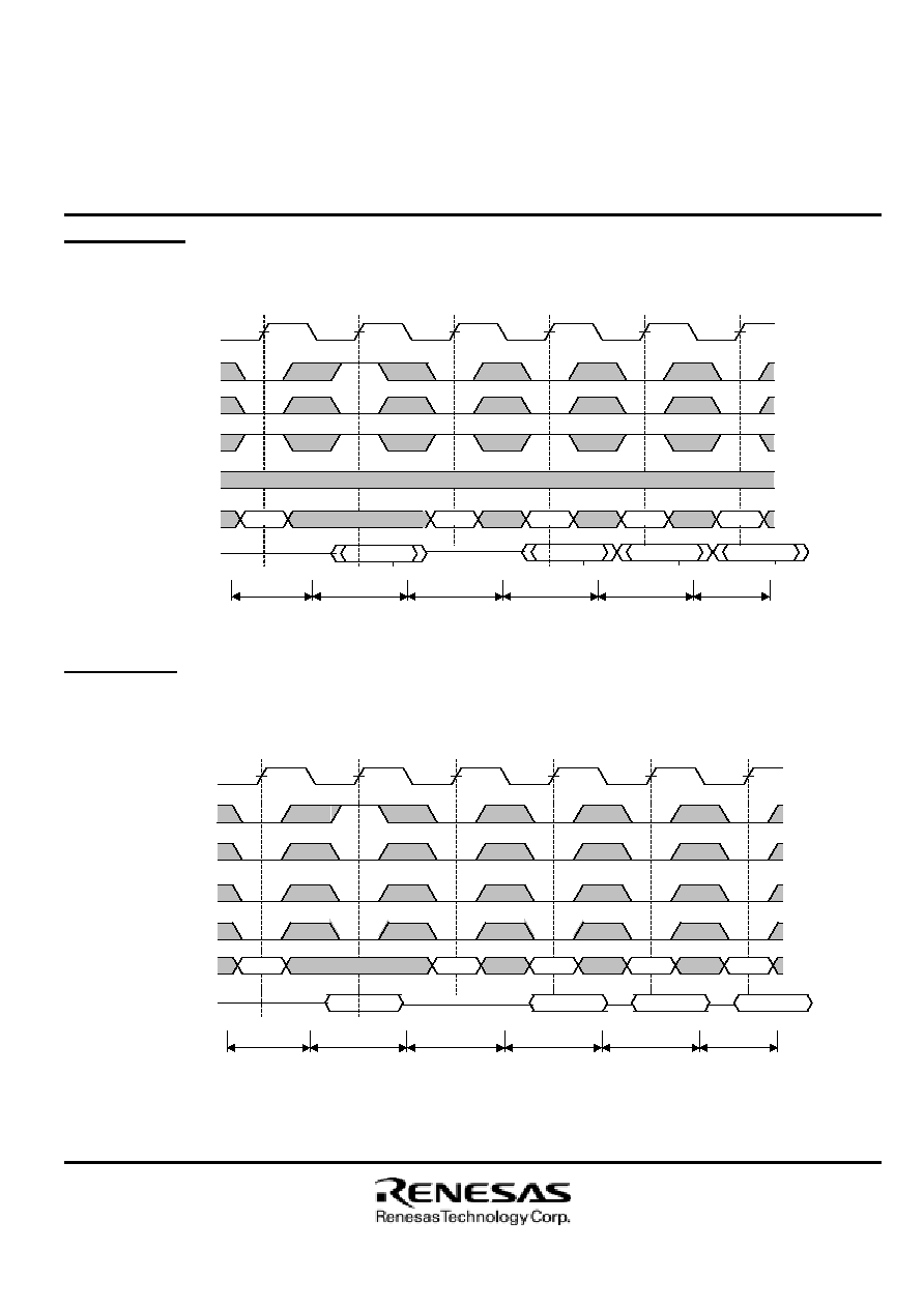
Read Operations Flow-Through Read
Read operation is initiated when the following conditions are satisfied at the rising edge of clock: All three chip enables (E1#, E2 and
E3#) are active, the write enable input signal (W#) is deasserted high, and ADV is asserted low.
Write Operation Single Late Write
Write operation occurs when the following conditions are satisfied at the rising edge of clock: All three chip enables (E1#, E2 and E3#)
are active, the write enable input signal (W#) is asserted low, and ADV is asserted low.
In Single Late Write the RAM requires Data in one rising clock edge later than the edge used to load Address and Control.
CLK
ADD
E1#
ADV
W#
BWx#
DQ
Q(A)
Q(B)
Read A
Deselect
Read B
Read C
Read D
Read E
A
B
C
D
E
Q(C)
#0
#1
#2
#3
#4
Q(D)
CLK
A
B
C
D
E
ADD
E1#
ADV
W#
BWx#
DQ
Write A
Deselect
Write B
Write C
Write D
Write E
D(A)
D(C)
D(B)
D(D)
#0
#1
#2
#3
#4