RT9231A
DS9231A-02 July 2001
www.richtek.com
1
Advanced PWM and Triple Linear Power Controller
General Description
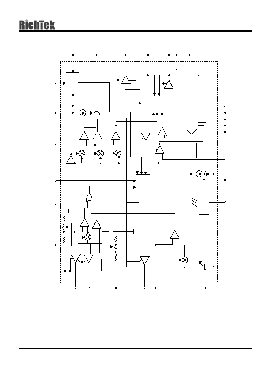
The RT9231A is a 4-in-one power controller
optimized for high-performance microprocessor and
computer applications. The IC integrates a PWM
controller, triple linear controller as well as monitoring
and protection functions into a 28-pin SOP package.
The PWM controller regulates the microprocessor
core voltage with a synchronous buck converter. The
first linear controller supplies the computer system's
AGP 1.5V or 3.3V bus power. The second linear
controller provides power for the 1.5V GTL bus and
the 3rd linear controller provides 1.8V power for the
North/South Bridge core voltage and/or cache
memory circuits.
The RT9231A features an Intel-compatible, TTL 5-bit
programmable DAC that adjusts the core voltage
from 2.1V to 3.5V in 0.1V increments and from 1.3V
to 2.05V in 0.05V steps. The 5-bit DAC has a typical
±
1% tolerance. The first linear controller is user-
selectable for output level of 1.5V and 3.3V with
±
2.5% accuracy. The other two linear controllers
provide fixed output voltages of 1.5V
±
3% and 1.8V
±
3%. All the three linear controllers drive external N-
MOSFET or NPNs bipolar for the pass transistor.
The RT9231A monitors all the output voltages. A
power-good signal is issued when the core voltage is
within
±
10% of the DAC setting and the other levels
are above their under-voltage levels. Additional build-
in over-voltage protection for the core output uses the
lower MOSFET to prevent output voltage above
115% of the DAC setting. The PWM over-current
function monitors the output current using the voltage
drop across the MOSFET's R
DS(ON)
,
which
eliminates the need for a current sensing resistor.
Applications
Full Motherboard Power Regulation for Computer
Low-voltage Distributed Power Supplies
Features
4-in-one Regulated Voltages for Microprocessor
Core, AGP Bus, North/South Bridge and/or
Cache Memory, GTL Bus Power
Compatible with HIP6021A
Power-good Output Voltage Monitor
Switching section
5-bit DAC Programmable from 1.3V to 3.5V
±
1% DAC Accuracy
Fast Transient Response
Full 0% to 100% Duty Cycle Driver
Fixed 200kHz Switching Frequency
Adaptive Non-overlapping Gate Driver
Over-current Monitor Uses MOSFET R
DS(ON)
Over-voltage Protection Uses Lower MOSFET
Linear Section
Fixed or User-adjustable Linear Regulator
Output Voltage
MOSFET and NPN Driving Capability
Ultra Fast Response Speed
Under-voltage Protection
Internal Thermal Shutdown
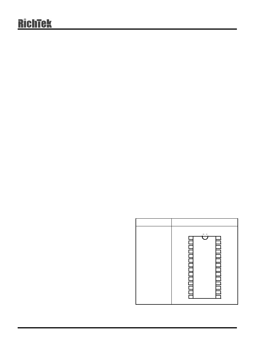
Pin Configurations
Part Number
Pin Configurations
RT9231ACS
(Plastic SOP-28)
TOP VIEW
1
2
3
4
5
6
7
8
9
10
11
12
17
18
19
20
21
22
23
24
25
26
27
28
13
14
16
15
FIX
VID4
VID3
VID2
VID1
VID0
PGOOD
SD
VSEN2
DRIVE2
SS
SELECT
FAULT
VSEN4
LGATE1
VCC
UGATE1
PHASE1
PGND
OCSET1
VSEN1
FB1
VSEN3
DRIVE3
GND
NC
VAUX
DRIVE4
RT9231A
www.richtek.com
DS9231A-02 July 2001
4
Absolute Maximum Ratings
Supply Voltage
+15V
PGOOD, FAULT and GATE Voltage
GND
-
0.3V ~ V
CC
+0.3V
Input, Output or I/O Voltage
GND
-
0.3V ~ 7V
Ambient Temperature Range
0
∞
C ~ +70
∞
C
Junction Temperature Range
0
∞
C ~ +125
∞
C
Storage Temperature Range
-
65
∞
C ~ +150
∞
C
Lead Temperature (Soldering, 10 sec.)
300
∞
C
Package Thermal Resistance
SOP-28,
JA
60
∞
C/W
Recommended Operating Conditions
Supply Voltage
+12V
±
10%
Ambient Temperature Range
0
∞
C to 70
∞
C
Junction Temperature Range
0
∞
C to 125
∞
C
CAUTION:
Stresses beyond the ratings specified in "Absolute Maximum Ratings" may cause permanent damage to the
device. This is a stress only rating and operation of the device at these or any other conditions above those
indicated in the operational sections of this specification is not implied.
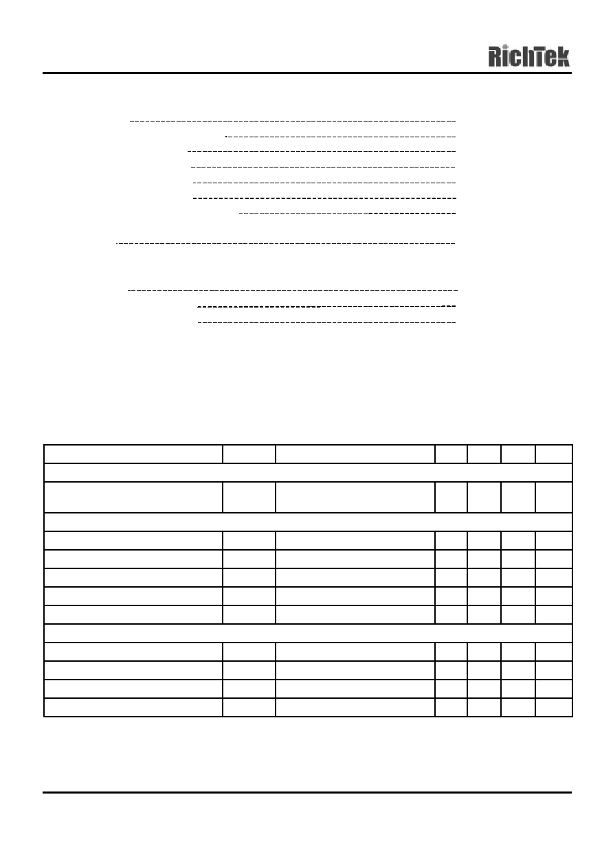
Electrical Characteristics
(V
CC
= 12V, PGND = 0V, T
A
= 25
∞
C, Unless otherwise specified.)
Parameter
Symbol
Test Conditions
Min
Typ
Max
Units
VCC Supply Current
Nominal Supply Current
I
CC
UGATE, LGATE, DRIVE2,
DRIVE3, and DRIVE4 Open
--
10
--
mA
Power-On Reset
VCC Rising Threshold
V
OCSET
= 4.5V
7.5
--
9.5
V
VCC Falling Threshold
V
OCSET
= 4.5V
7
--
9
V
Rising VAUX Threshold
V
OCSET
= 4.5V
--
2.8
--
V
VAUX Threshold Hysteresys
V
OCSET
= 4.5V
--
0.5
--
V
Rising V
OCSET
Threshold
--
1.25
--
V
DAC and Band Gap Reference
DAC (VID0-VID4) Input Low Voltage
--
--
0.8
V
DAC (VID0-VID4) Input High Voltage
2.0
--
--
V
DACOUT Voltage Accuracy
-1
--
1
%
Band Gap Reference Voltage
V
BG
1.240 1.265 1.290
V
To be continued

RT9231A
DS9231A-02 July 2001
www.richtek.com
5
Parameter
Symbol
Test Conditions
Min
Typ
Max
Units
Oscillator
Free Running Frequency
180
200
225
kHz
Ramp Amplitude
V
OSC
--
1.9
--
V
P-P
Linear Regulators (OUT2, OUT3, and OUT4)
VSEN2 Regulation Voltage
SELECT
<
0.8V
1.462 1.500 1.538
V
VSEN2 Regulation Voltage
SELECT
>
2.0V
3.500 3.600 3.700
V
VSEN3 Regulation Voltage
1.455 1.500 1.545
V
VSEN4 Regulation Voltage
1.746 1.800 1.854
V
Under-Voltage Level
(All Linears) (VSEN/VREG)
VSEN3 Rising
--
75
--
%
Under-Voltage Hysteresis
(All Linears) (VSEN/VREG)
VSEN3 Falling
--
100
--
mV
Output Drive Current (All Linears)
VAUX = 5V
20
40
--
mA
Synchronous PWM Controller Error Amplifier
DC Gain
--
65
--
dB
PWM Controller Gate Driver
UGATE Source
R
UGATE
VCC = 12V
VCC-V
UGATE
= 1V
--
4
7
UGATE Sink
R
UGATE
V
UGATE
= 1V
--
3
7
LGATE Source
I
LGATE
VCC = 12V, V
LGATE
= 2V
--
1
--
A
LGATE Sink
R
LGATE
V
LGATE
= 1V
--
2
6
Protection
V
OUT1
Over-Voltage Trip
VSEN1 Rising
112
115
124
%
FAULT Souring Current
V
FAULT
= 8V
10
14
--
mA
OCSET1 Current Source
I
OCSET
V
OCSET1
= 4.5V
170
200
230
µ
A
Soft-Start Current
I
SS
V
SS
= 1V
--
28
--
µ
A
Power Good
V
OUT1
Upper Threshold
VSEN1 Rising
108
--
112
%
V
OUT1
Under Voltage
VSEN1 Rising
87
--
95
%
V
OUT1
Hysteresis (VSEN1/DACOUT)
Upper/Lower Threshold
--
2
--
%
PGOOD Voltage Low
V
PGOOD
I
PGOOD
= -4mA
--
--
0.5
V