R5532V002
2003.Mar.14
Rev. 1.00
- 1 -
Dual Slot PCMCIA Power Controller
I
I
I
IDESCRIPTION
The R5532V002 switches between the three VCC voltages (0V/3.3V/5.0V) and the V
PP
voltages (off/0V/3.3V/5.0V).
The R5532V002 has two sets of VCC output and VPP output each, therefore it fits dual slot models. If VCC pin or
VPP pin may be clamped to the GND, short current limit works at 1A(Min.) for VCC and 0.2A(Min.) for VPP.
The R5532V002 is suitable for standard PCMCIA power controllers.
I
I
I
IFEATURES
Low on resistance P-channel MOSFET Switch
Dual Slot Power Supply Control
Over- Current Limit Protection
Thermal Shutdown Protection
Low Consumption Current
Break-Before-Make Switching
SSOP-28 pin Package
I
I
I
IAPPLICATIONS
Dual Slot PC card Power Supply Pin Voltage Switch
Card-bus Slot Power Supply Control
PC Card Reader/Writer
I
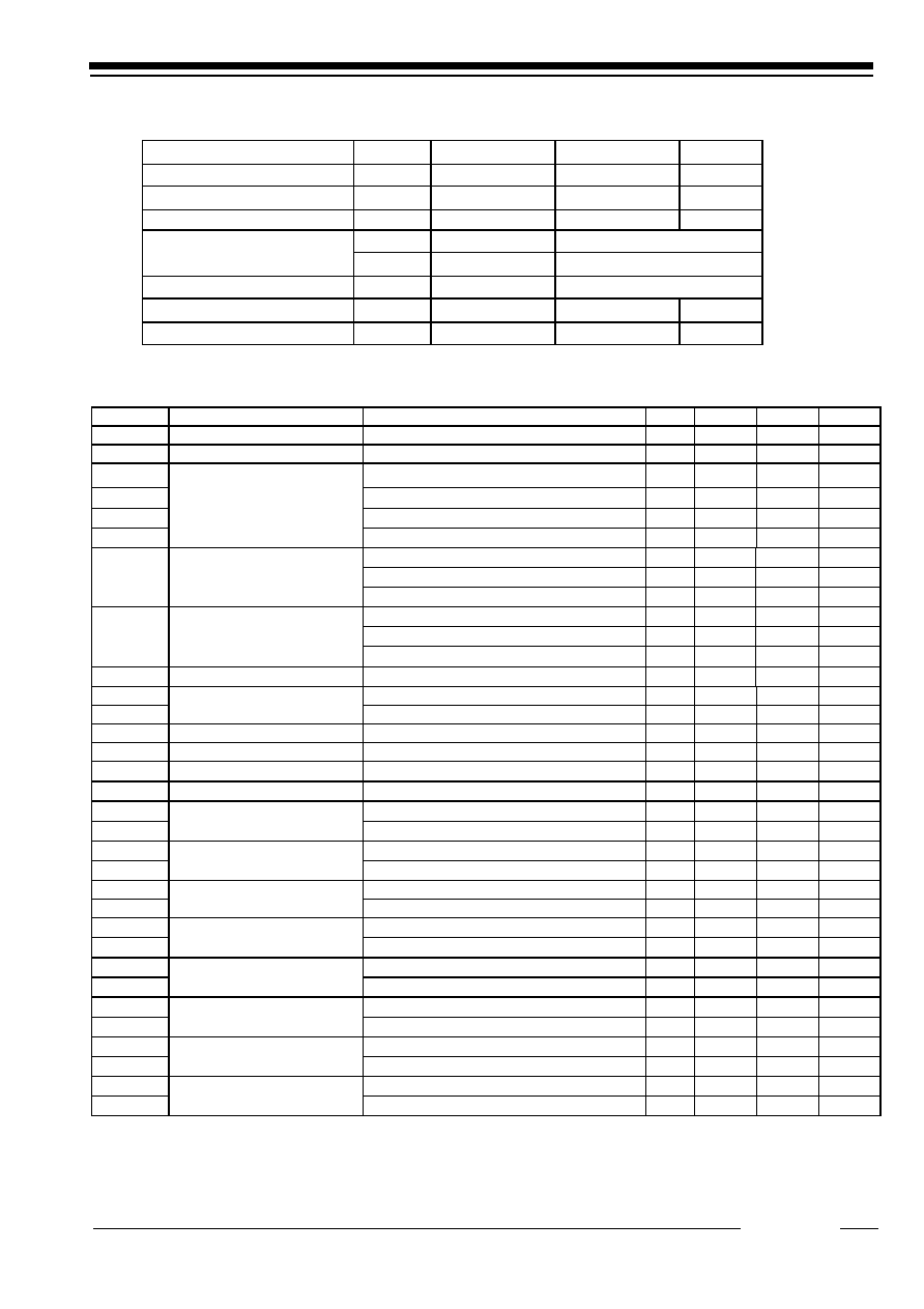
PIN CONFIGURATION
AVcc3IN
AVccOUT
AVccOUT
BEN0
GND
AEN1
AVcc5IN
AVcc5_EN
AVccOUT
AVppOUT
BEN1
AEN0
1
2
3
4
5
6
7
8
28
27
26
25
24
23
22
21
BVccOUT
BVppOUT
NC
9
10
11
12
BVcc5IN
GND
BVccOUT
20
19
18
17
AVcc5IN
AVcc3_EN
BVcc3IN
BVcc5_EN
BVcc3_EN
BVcc5IN
BVccOUT
13
14
16
15
NC
NC
NC
12345
Rev. 1.00
- 3 -
I
ABSOLUTE MAXIMUM RATINGS
Topt=25
∞C
Item
Symbol
Conditions
Ratings
Unit
Input Voltage(5V)
V
cc5IN
-0.3 to 6.0
V
Input Voltage(3V)
V
cc3IN
-0.3 to 6.0
V
Logic Input Voltage
V
IN
-0.3 to 6.0
V
I
O(VCC)
Each Slot
>1A, Internally limited
Output Current
I
O(VPP)
Each Slot
>200mA, Internally limited
Power Dissipation
P
D
Internally limited
Operating Temperature Range
Topt
-40 to 85
∞C
Storage Temperature Range
Tstg
-55 to 125
∞C
I
ELECTRICAL CHARACTERISTICS
Topt=25
∞C
Symbol
Item
Conditions
Min.
Typ.
Max.
Unit
V
cc5
Supply Voltage(5V)
3.0
5.0
5.5
V
V
cc3
Supply Voltage(3V)
3.0
3.3
5.5
V
I
cc5
Vcc
OUT
= 5V or 3.3V
30
60
µA
I
SLP5
Vcc
OUT
= 0V (sleep mode)
0.2
10.0
µA
I
CC3
Vcc
OUT
= 5V or 3.3V
10
30
µA
I
SLP3
Supply Current(each slot)
Vcc
OUT
= 0V (sleep mode)
0.1
10.0
µA
Select Vcc
OUT
=5V
85
140
m
Select Vcc
OUT
=3.3V
100
150
m
RoV
cc
Vcc
OUT
switch resistance
Select Vcc
OUT
=0V
500
3900
Select Vpp
OUT
=5V
1.8
2.5
Select Vpp
OUT
=3.3V
3.3
5.0
RoV
pp
Vpp
OUT
switch resistance
Select Vpp
OUT
=0V
2500
3900
I
PPL
Vpp
OUT
Leakage Current
Select Vpp
OUT
=Hi-Z
1
10
µA
I
CCSC
Vcc
OUT
=0V
1
1.4
A
I
PPSC
Short Current Limit
V
PP OUT
=0V
0.2
0.3
A
V
IH
Logic Input "H" Voltage
2.2
6.0
V
V
IL
Logic Input "L" Voltage
-0.3
0.8
V
I
IN
Logic Input Current
0V<V
IN
<5.5V
-1
1
µA
T
SD
Thermal Shutdown Temperature
135
∞C
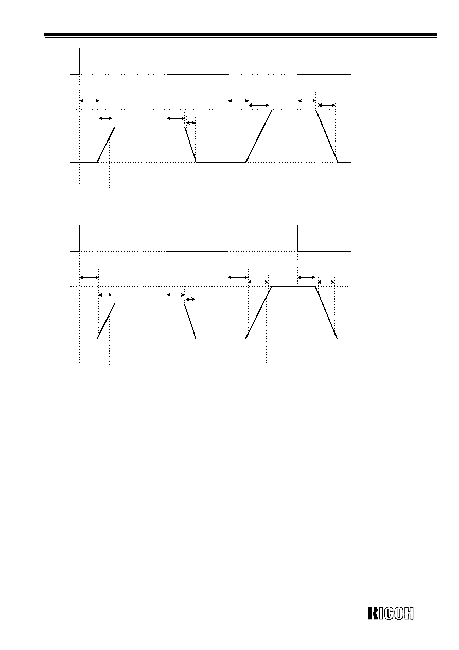
t1
Vcc
OUT
=0V to 10% of 3.3V
300
1500
µs
t
2
Vcc Turn-on Delay Time
(*Note 2)
Vcc
OUT
=0V to 10% of 5.0V
500
3000
µs
t
3
Vcc
OUT
=10% to 90% of 3.3V
200
800
2500
µs
t
4
Vcc Rising Time (*Note 2)
Vcc
OUT
=10% to 90% of 5.0V
200
1800
6000
µs
t
7
Vcc
OUT
=3.3V to Hi-Z
2.3
8.0
ms
t
8
Vcc Turn-off Delay Time
(*Note1,2,4)
Vcc
OUT
=5V to Hi-Z
2.8
8.0
ms
t5
Vcc
OUT
=90% to 10% of 3.3V
100
700
1500
µs
t6
V
cc
Falling Time (*Note 2)
Vcc
OUT
=90% to 10% of 5.0V
100
600
2000
µs
t9
Vpp
OUT
=0V to 10% of 3.3V
15
50
µs
t10
Vpp Turn-on Delay Time
(*Note 3)
Vpp
OUT
=0V to 10% of 5.0V
25
50
µs
t11
Vpp
OUT
=10% to 90% of 3.3V
100
200
800
µs
t12
Vpp Rising Time (*Note 3)
Vpp
OUT
=10% to 90% of 5.0V
100
280
1000
µs
t15
Vpp
OUT
=3.3V to Hi-Z
0.1
1.0
µs
t16
Vpp Turn-off Delay Time
(*Note 1,3)
Vpp
OUT
=5V to Hi-Z
0.1
1.0
µs
t13
Vpp
OUT
=90% to 10% of 3.3V
0.05
1.00
µs
t14
Vpp Falling Time (*Note 3)
Vpp
OUT
=90% to 10% of 5.0V
0.05
1.00
µs
(*Note1) Delay from commanding Hi-Z or 0V to beginning slope
(*Note2) t1 to t8 Test Condition: RL=10
(*Note3) t9 to t15 Test Condition: RL=100
(*Note4) Do not apply to current limit or thermal shutdown conditions during these terms
12345
Rev. 1.00
- 5 -
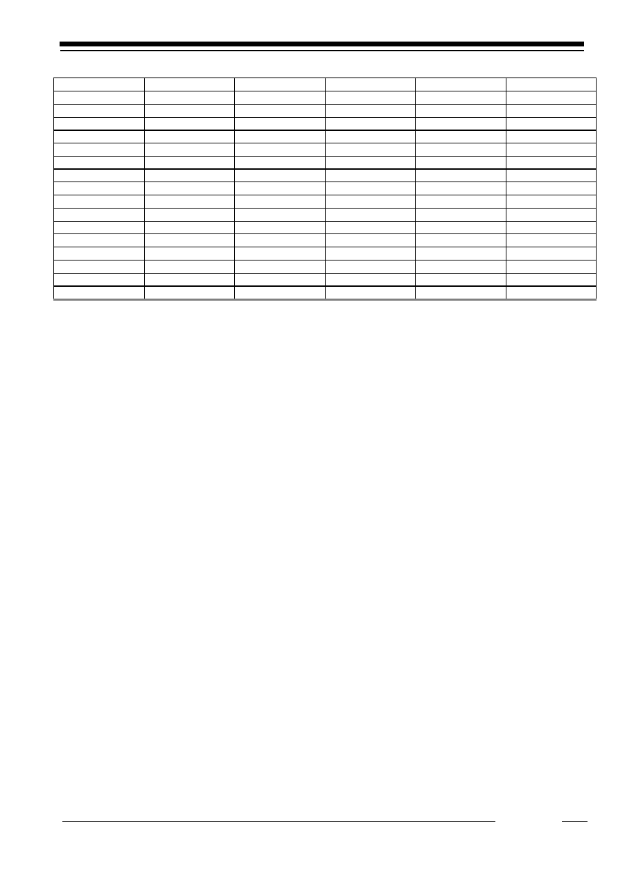
R5532V002 Control Logic Table
Vcc
5_EN
Vcc
3_EN
EN1
EN0
Vcc
OUT
Vpp
OUT
0
0
0
0
0V
0V
0
0
0
1
0V
Hi-Z
0
0
1
0
0V
Hi-Z
0
0
1
1
0V
Hi-Z
0
1
0
0
5V
0V
0
1
0
1
5V
5V
0
1
1
0
5V
Hi-Z
0
1
1
1
5V
Hi-Z
1
0
0
0
3.3V
0V
1
0
0
1
3.3V
3.3V
1
0
1
0
3.3V
Hi-Z
1
0
1
1
3.3V
Hi-Z
1
1
0
0
0V
0V
1
1
0
1
0V
Hi-Z
1
1
1
0
0V
Hi-Z
1
1
1
1
0V
HI-Z
I
OPERATION
When the VCCOUT =0V is selected, the IC switches into the sleep mode, and draws only nano-amperes of leakage current.
Without being V
CCOUT
=0V, if commanded to immediately switch from 5V to 3.3V or vice versa, enhancement of the second
switch begins after the first is OFF, realizing break-before-make protection.
In case that an OUT pin may be clamped to the GND, if over-current would continue, the temperature of the IC would increase
drastically. If the temperature of the IC is beyond 135
∞C, the switch transistor turns off. Then, when the temperature of the IC
decreases equal or lower than 125
∞C, the switch transistor turns on. Unless the abnormal situation of OUT pin is removed or
make them be disable, the switch transistor repeats on and off.
Short over-current level is set internally in the IC. There are three types of response against over-current:
xUnder the condition
that OUT pin is short or large capacity is loaded, if the IC is enabled, the IC becomes constant current state. Current level of
constant current is short current limit.
yWhile the switch transistor is on, if OUT pin is short or large capacity is loaded, until
the current limit circuit responds, large transient current flows. After the transient current is beyond the current limit threshold
and current limit circuit responds, the IC becomes into the constant current mode.
zIn the case that load current gradually
increases, the IC is not into the constant current state until the current is beyond over current limit. Once the level is beyond the
over current detector threshold, load current is limited into short current limit level. Note that load current continuously flows
until the load current is beyond the over-current detector threshold.
I
I
I
IAPPLICATION NOTES
* V
CC5IN
voltage should be equal or more than V
CC3IN
.
* Same name pins should be connected one another.
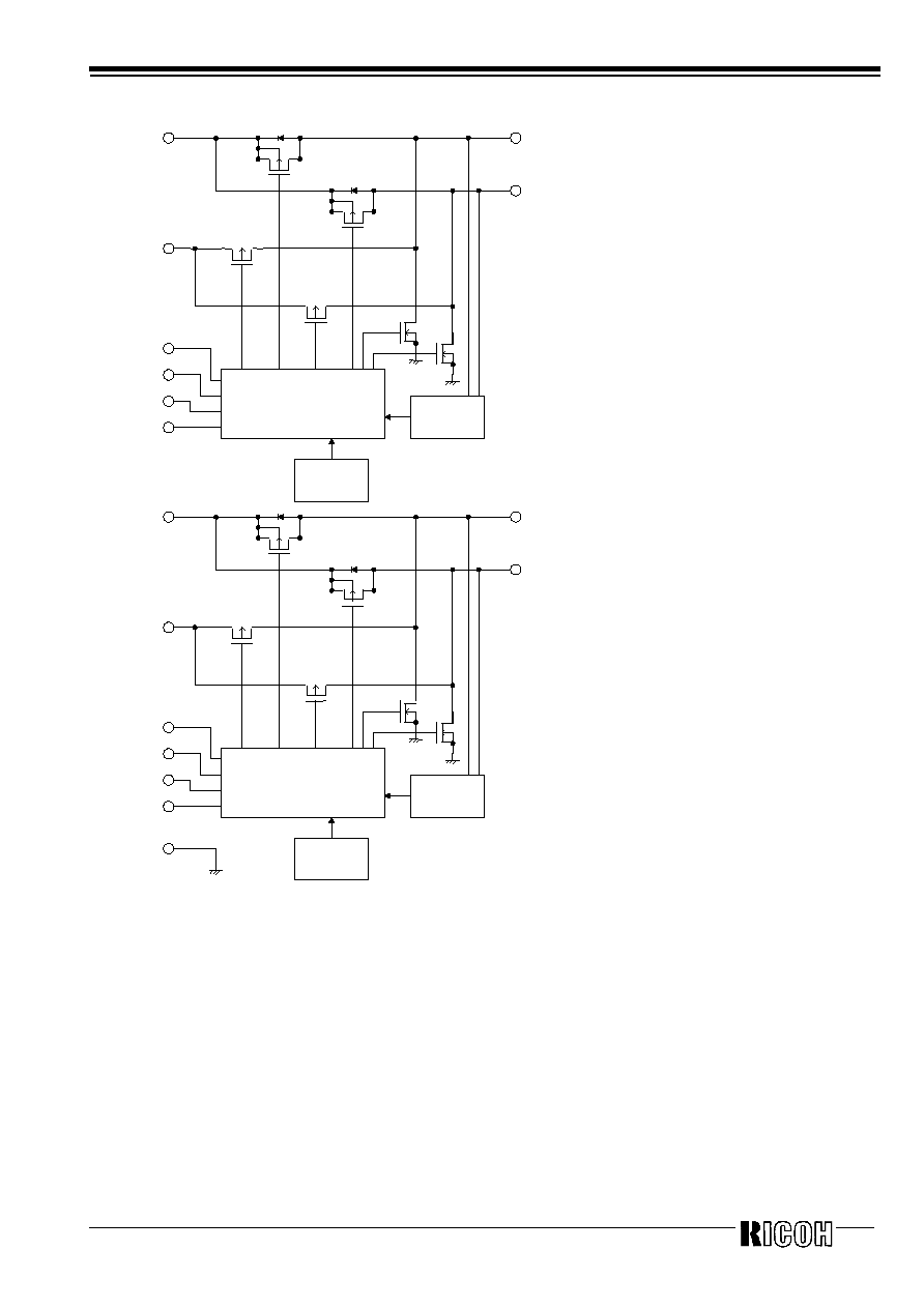
* There is a parasitic diode between source and drain of the switch transistors. (Refer to the block diagram.)
Therefore, even If the switch may be disabled, in case the OUT voltage is higher than V
CC5IN
, some current flows
from OUT to V
CC5IN
.