BH2221FV
Standard ICs
1/6
8bit 12ch D/A converter
BH2221FV
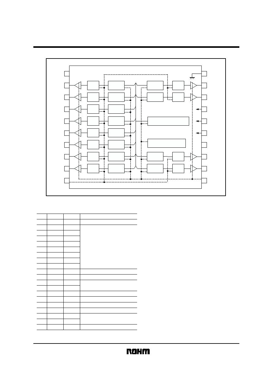
BH2221FV is an 8bit D/A converter for electronic adjustment. The 12-channel DC output voltage can be independently
controlled by three-wire serial interface from micro-controller. The D/A converter can generate without loss by Rail-to-Rail
output within the setting voltage. The built-in power ON reset circuit keeps the output state Low after the power is ON and
prevents the unstable output state.
!
!
!
!
Applications
The voltage adjustment for DVC, DSC etc.
!
!
!
!
Features
1) 8bit 12-channel D/A converters adopting R-2R system.
2) The full scale output voltage range : 2.7V
5.5V.
3) 3-wire 12-bit serial interface.
4) POWER ON RESET circuit.
5) SSOP-B20 package.
!
!
!
!
Absolute maximum ratings (Ta=25
°C)
Parameter
Symbol
Limits
Unit
Power supply voltage
V
CC
-
0.3~
+
7.0
V
Maximum output voltage
V
IN
-
0.3~V
CC
V
Storage temperature
Tstg
-
55~
+
125
°
C
Power dissipation
Pd
400
mW
Reduced by 4mW for each increase in Ta of 1
°
C over 25
°
C.
This product is not designed for protection against radioactive rays.
!
!
!
!
Recommended operating conditions (Ta=25
°C)
Parameter
Symbol
Typ.
Max.
Unit
V
CC
supply voltage
V
CC
-
5.5
V
-
1.0
Analog output source current
I
OL
mA
-
1.0
mA
Analog output sink current
I
OH
-
85
°
C
Operating temperature range
Topr
-
0.1
Limit load capacitance
Please set to V
CC
V
DD
.
CL
µ
F
Min.
2.7
V
DD
supply voltage
V
DD
-
V
CC
V
2.7
-
-
-
20
-
-
1.0
-
Clock frequency
FSCLK
MHz
BH2221FV
Standard ICs
3/6
!
!
!
!
Electrical characteristics (unless otherwise noted, Ta=25
°C, V
CC
=3.0V, V
DD
=3.0V, R
L
=OPEN, C
L
=0pF)
Parameter
Symbol
Min.
Typ.
Max.
Unit
Conditions
<Operating current
> (
80H set)
V
CC
system
V
DD
system
<Logic interface
>
Input low voltage
Input high voltage
Input low current
Input high current
<Buffer amplifier
>
Minimum output voltage
Maximum output voltage
<DAC accuracy
>
Resolution
Differential nonlinearity error
Nonlinearity error
I
CC
I
DD
V
IL
V
IH
I
IL
I
IH
ZS1
ZS2
ZS3
FS1
FS2
FS3
RES
DNL
INL
-
-
GND
0.8V
CC
-
-
GND
GND
GND
V
CC
-
0.1
V
CC
-
0.2
V
CC
-
0.3
-
-
1.0
-
1.5
0.6
1.0
-
-
-
-
-
-
-
-
-
-
8
-
-
1.5
2.0
0.2V
CC
V
CC
10
10
0.1
0.2
0.3
V
CC
V
CC
V
CC
-
1.0
1.5
mA
mA
V
V
µ
A
µ
A
V
V
V
V
V
V
bit
LSB
LSB
CLK=1MHz
00H set I
OH
=0.0mA
00H set I
OH
=0.5mA
00H set I
OH
=1.0mA
FFH set I
OL
=0.0mA
FFH set I
OL
=0.5mA
FFH set I
OL
=1.0mA
Input code 02H~FDH
Input code 02H~FDH
!
!
!
!
Circuit operation
(1) Power on reset
This LSI has a power on reset circuit that sets an analog output to low level in V
CC
power stand-up.
Please be sure that the time constant meets below condition, because the output is undefined when V
CC
power stand
up too rapidly.
Power on reset voltage
VPOR
V
-
1.9
-
V
CC
=0
2.7V
V
CC
supply voltage rise time
trV
CC
10
ms
-
-
Parameter
Conditions
Symbol
Min.
Typ.
Max.
Unit
BH2221FV
Standard ICs
5/6
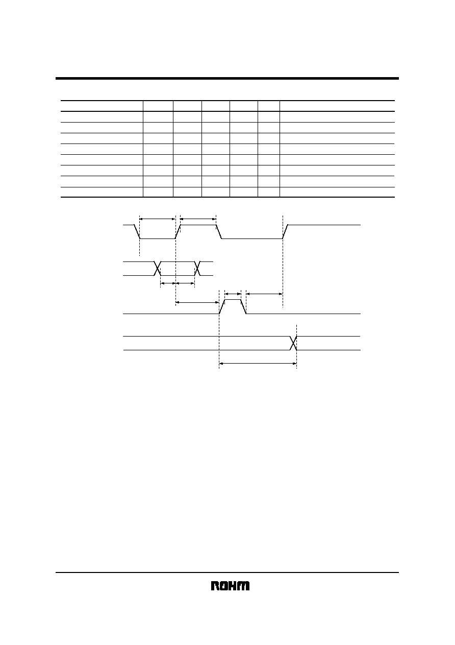
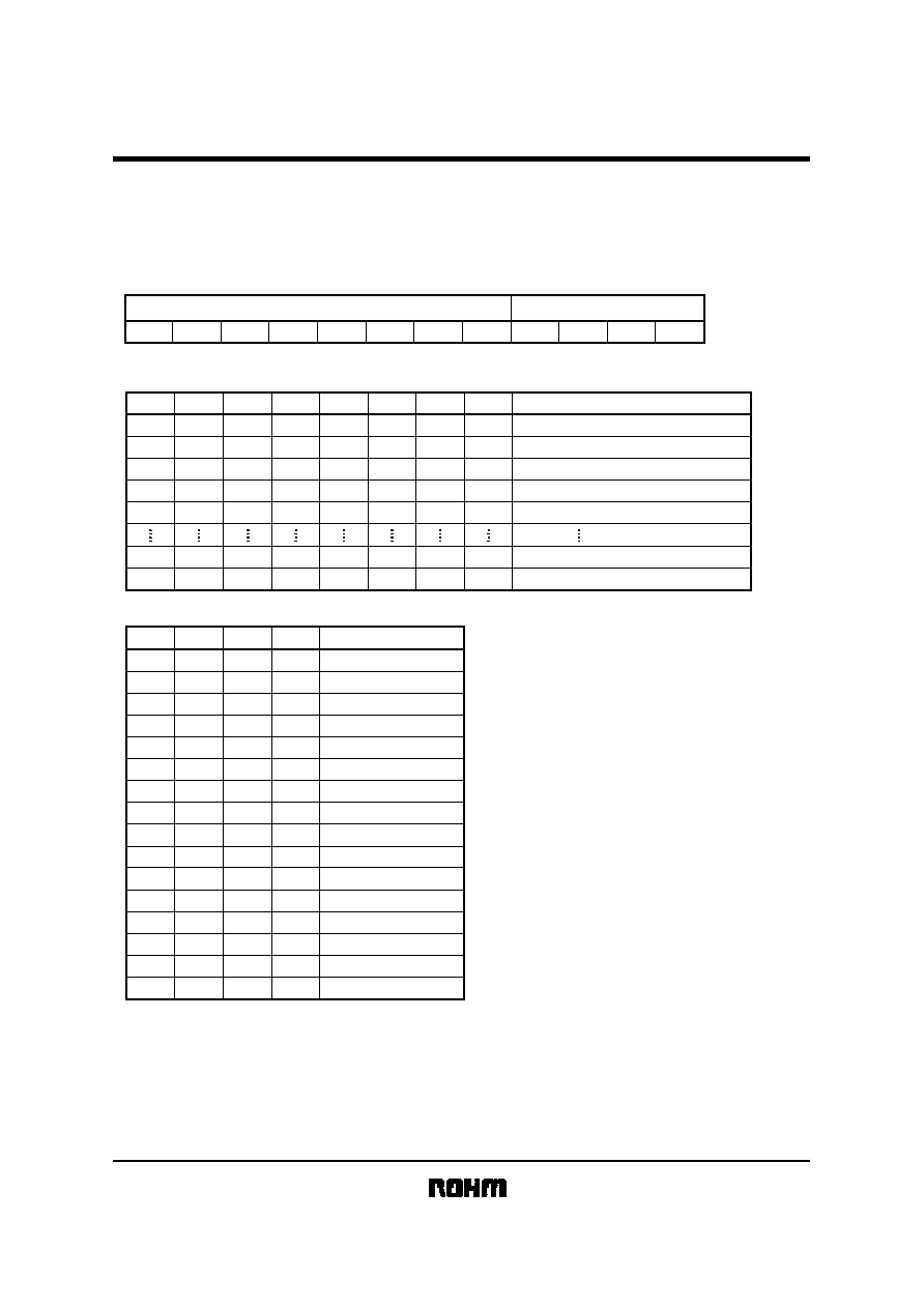
(3) Command sending
Control command is 3wire 12bit serial interface. (MSB first)
Data is taken in with the rise edge of the CLK and output data is fixed in the LD high section.
Data is maintained in the LD low section.
Analog output voltage level
Data set
Channel select
Don't Care
Don't Care
Don't Care
AO11
AO12
AO1
AO2
AO5
AO6
AO7
AO8
AO9
AO10
GND
(V
CC
-GND) / 256
×
1
(V
CC
-GND) / 256
×
2
(V
CC
-GND) / 256
×
3
(V
CC
-GND) / 256
×
4
(V
CC
-GND) / 256
×
254
(V
CC
-GND) / 256
×
255
0
1
0
0
1
0
1
D0
0
0
0
1
1
1
1
D1
D0
LSB (LAST)
·
Data set
·
Channel select
MSB (FIRST)
D1
D2
D3
D4
D5
D6
D7
D8
D9
0
0
0
0
1
1
1
D2
0
0
0
0
0
1
1
D3
0
0
0
0
0
1
1
D4
0
0
0
0
0
1
1
D5
0
0
0
0
0
1
1
D6
0
0
0
0
0
1
1
D7
D10
D11
Don't Care
AO3
AO4
Adress select
0
0
0
0
0
1
1
1
1
1
1
1
1
0
0
0
D8
0
0
0
0
0
0
1
1
1
1
1
1
1
0
0
1
D9
0
1
0
0
1
1
0
1
1
0
0
1
1
0
1
0
D10
0
1
0
1
0
1
0
1
0
1
0
1
0
1
0
1
D11