 | –≠–ª–µ–∫—Ç—Ä–æ–Ω–Ω—ã–π –∫–æ–º–ø–æ–Ω–µ–Ω—Ç: BH7273KV | –°–∫–∞—á–∞—Ç—å:  PDF PDF  ZIP ZIP |
1
Video ICs
Equalizer and ATF circuit IC for
Digital VCRs
BH7273KV
The BH7273KV is an equalizer and ATF circuit IC developed for use with digital video cassettes (DVC). By using this
IC, it is simple to design the filter for the equalizer required for DVD sets. In addition, the ATF circuit detects the pilot
signals and generates error signals.
∑
Applications
Equalizers and ATFs for digital VCRs
∑
Features
1) Enables the configuring of all pass filters, 1 + D cir-
cuits, and transversal filters (TVF).
2) Built-in VCA, amplifier, buffer, and mixer amplifier.
3) Detects the ATF pilot signal and generates an ATF
error signal.
4) Built-in 1.5MHz LPF, VCA, 465kHz BPF, 697.5kHz
BPF, 25dB amplifier, peak detector, and subtractor.
5) Intermediate frequencies are variable by controlling
the voltages for the 465kHz BPF and 697.5kHz
BPF.
∑
Absolute maximum ratings (Ta = 25∞C)
∑
Recommended operating conditions (Ta = 25∞C)
Parameter
Symbol
Limits
Unit
Applied voltage
Power dissipation
Operating temperature
Storage temperature
V
CC
Pd
Topr
Tstg
7.0
1000
≠ 20 ~ + 65
≠ 55 ~ + 125
V
mW
∞
C
∞
C
When mounted on a 70mm
◊
70mm
◊
1.6mm glass epoxy board.
Reduced by 10.0mW for each increase in Ta of 1
∞
C over 25
∞
C.
Parameter
Symbol
Min.
Typ.
Max.
Unit
Conditions
Power supply voltage
V
CC
5V
4.6
4.9
5.2
V
2, 15, 21, 33, 44, 48, 60pin
Not designed for radiation resistance.

2
Video ICs
BH7273KV
∑
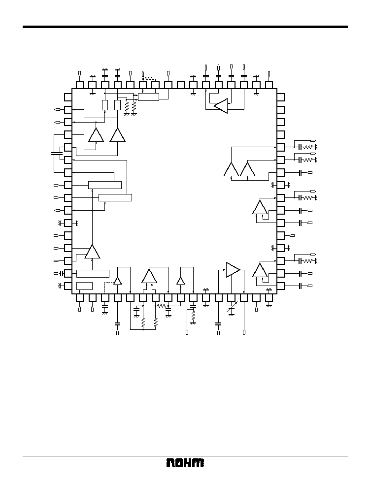
Block diagram
47
46
45
44
43
42
41
40
39
38
37
36
35
34
33
48
60
61
62
63
64
59
58
57
56
55
54
53
52
51
50
49
32
31
30
29
28
27
26
25
24
23
22
21
20
19
18
17
14
13
12
16
15
11
10
9
8
7
6
5
4
3
2
1
DET
DET
AMP
VCA
AMP
AMP 25dB
14 / 24dB
47k 47k
SUBTRACT
697.5kHz BPF
465.0kHz BPF
1.5MHz LPF
CTRL
VCA
AMP
AMP
BF
BF
Mix
BH7273KV
Vcc 4.9V
GND
F2 DET OUT
F1 DET OUT
Vcc 4.9V
SUBSTRACT OUT
OFFSET BIAS OUT
OFFSET BIAS
N.C.
GND
MIX + OUT
MIX ≠ OUT
MIX IN2
MIX IN1
GND
Vcc 4.9V
N.C.
F1 AMP OUT
F2 AMP OUT
F2 AMP IN
F1 AMP IN
F1 BPF OUT
F2 BPF OUT
F2 adj
F1 adj
GCA OUT
GND
Vcc 4.9V
GAIN adj
GAIN SW
ATF IN
GND
N.C.
N.C.
N.C.
N.C.
BF OUT2
BF OUT1
BF IN
GND
TVF2AMP OUT
TVF2AMP ≠ IN
TVF2AMP + IN
Vcc 4.9V
GND
TVF1AMP OUT
TVF1AMP ≠ IN
TVF1AMP + IN
SLEEP CTRL
Vcc 4.9V
BIAS FILTER
BF2 IN
BF2 OUT
APF1AMP + IN
APF1AMP ≠ IN
APF1AMP OUT
DRIVER IN
DRIVER OUT
GND
TVF1VCA + IN
TVF1CTRL
TVF1VCA OUT
Vcc 4.9V
GND
∑
Vcc-GND pin table
Pin No.
Pin name
Function
2
11
V
CC
4.9V
GND
All pass filter for pins 3 to 10
Same as above
15
16
V
CC
4.9V
GND
12-14pin VCA, 17-19pin AMP
Same as above
33
34
V
CC
4.9V
GND
35-38pin MIX AMP
35-38pin MIX AMP
44
39
V
CC
4.9V
GND
Detector, subtractor circuit
Same as above
48
47
V
CC
4.9V
GND
BPF, 25dBAMP
Same as above
60
59
V
CC
4.9V
GND
LPF, GCA
Same as above
64
GND
N.C.
(Connected to GND to lower impedance)
21
20
25
V
CC
4.9V
GND
GND
22-24pin AMP, 26-28pin BUFF
22-24pin AMP
26-28pin BUFF
Make sure that Vcc and GND do not sway.
Separate the equalizer and ATF grounds.
Since the gain of the ATF circuit is high, make sure that there is no return from the output to input.
3
Video ICs
BH7273KV
∑
Electrical characteristics (unless otherwise noted, Ta = 25∞C, V
CC
= 4.9V, f = 4.0MHz)
Parameter
Symbol
Min.
Typ.
Max.
Unit
Conditions
Voltage gain
Frequency characteristics
VCA
TVF AMP
Voltage gain
Voltage gain
Frequency characteristics
G
VA
G
VA
≠ 3.0
≠ 3.0
±
0.0
±
0.0
+ 3.0
dB
dB
Input at pin 4 = 300mV
P-P
Measure output at pin 10
f = 8.0 / 1.0MHz, V
IN
= 300mV
P-P
Output level difference for pin 10
G
VV1
G
VV2
G
VV
≠ 1.0
--
≠ 3.0
≠ 28.0
--
--
dB
dB
dB
Input at pin 12 = 150mV
P-P
, pin 13 = 3.0V
Measure output at pin 14
Input at pin 12 = 150mV
P-P
, pin 13 = 0.25V
Measure output at pin 14
f = 8.0 / 1.0MHz, V
IN
= 150mV
P-P
Output level difference for pin 14; pin 13 = 3.0V
Voltage gain
Frequency characteristics
G
VT
G
VT
≠ 3.0
±
0.0
9.9
--
dB
dB
Input at pins 17, 18, 22, and 23 = 150mV
P-P
Measure output at pins 19 and 24
f = 8.0 / 1.0MHz, V
IN
= 150mV
P-P
Output level difference for pins 19 and 24
BUFF AMP
Voltage gain
Frequency characteristics
G
VB
G
VB
≠ 4.2
≠ 3.0
≠ 1.2
±
0.0
--
--
dB
dB
Input at pin 26 = 300mV
P-P
Measure output at pins 27 and 28
f = 8.0 / 1.0MHz, V
IN
= 300mV
P-P
Output level difference for pins 27 and 28
Quiescent current
Quiescent current
[Equalizer block]
All pass filter
Iq
Iq
(S)
--
--
63
16
100
30
mA
mA
No signal
No signal, sleep mode
--
≠ 12.0
MIX AMP
Voltage gain
Frequency characteristics
[ATF block]
VCA voltage gain 1
VCA voltage gain 2
465.0kHz BPF voltage gain
697.5kHz BPF voltage gain
G
VM
G
VM
5.0
8.0
0.0
11.0
--
dB
dB
ATF OUT output level 1
V
ATF1
1.30
1.50
1.70
V
Input at pins 35 and 36 = 150mV
P-P
Measure output at pins 37 and 38
f = 8.0 / 1.0MHz, V
IN
= 150mV
P-P
Output level difference for pins 37 and 38
G
VF1
G
VF2
G
VB1
G
VB2
11
21
44
44
14
24
48
48
17
27
52
52
dB
dB
dB
dB
ATF OUT output level 2
ATF OUT output level 3
V
ATF2
V
ATF3
1.50
0.60
1.80
0.90
2.10
1.20
V
V
Input at pin 63 = 2.0mV
P-P
, pin 62 = low
Measure output at pin 58, f = 697.5kHz
Input at pin 63 = 2.0mV
P-P
, pin 62 = high
Measure output at pin 58, f = 697.5kHz
Input at pin 63 = 0.3mV
P-P
, pin 62 = high
Measure output at pin 50, f = 465.0kHz
Input at pin 63 = 0.3mV
P-P
, pin 62 = high
Measure output at pin 51, f = 697.5kHz
50pin = 100mV
P-P
51pin = 300mV
P-P
, 41pin = 1.5V
50pin = 500mV
P-P
51pin = 100mV
P-P
, 41pin = 1.5V
No signal
[Logic block]
SLEEP hold voltage
SLEEP hold voltage
VCA gain switch low
VCA gain switch high
V
TH1H
V
TH1L
V
TH62L
V
TH62H
2.0
0.0
0.0
2.0
--
--
--
--
4.9
1.0
1.0
4.9
V
V
V
V
Pin 1 voltage for SLEEP mode
Pin 1 voltage for SLEEP mode
Pin 62 voltage for ATF VCA gain to be low
Pin 62 voltage for ATF VCA gain to be high
≠ 3.0
±
0.0
2.0
3.9
6.9
4
Video ICs
BH7273KV
∑
Measurement circuit
47
46
45
44
43
42
41
40
39
38
37
36
35
34
33
48
60
61
62
63
64
59
58
57
56
55
54
53
52
51
50
49
32
31
30
29
28
27
26
25
24
23
22
21
20
19
18
17
14
13
12
16
15
11
10
9
8
7
6
5
4
3
2
1
DET
DET
AMP
VCA
AMP
AMP 25dB
14 / 24dB
47k 47k
SUBTRACT
697.5kHz BPF
465.0kHz BPF
1.5MHz LPF
CTRL
VCA
AMP
AMP
BF
BF
MIX
BH7273KV
Fig. 1
Vcc 4.9V
ATF OUT
Offset BIAS
MIX OUT
MIX OUT
MIX IN
MIX IN
465.0kHz
BPF OUT
697.5kHz
BPF OUT
BUFF OUT
BUFF OUT
BUFF IN
TVF AMP OUT
TVF AMP IN
TVF AMP IN
TVF AMP IN
TVF AMP IN
TVF AMP OUT
Vcc 4.9V
Vcc 4.9V
Vcc 4.9V
1000p
2.2k
0.1
µ
0.1
µ
0.1
µ
0.1
µ
f2 adj
f1 adj
ATF VCA OUT
0.1
µ
0.1
µ
0.1
µ
1000p
0.1
µ
300
300
600
600
0.1
µ
0.1
µ
0.1
µ
0.1
µ
0.1
µ
0.1
µ
0.1
µ
0.1
µ
0.1
µ
0.1
µ
0.1
µ
600
470
1k
47p
300
33p
0.1
µ
Vcc 4.9V
Vcc 4.9V
Vcc 4.9V
Gain adj
Gain SW
ATF IN
SLEEP
VCA OUT
APF OUT
VCA IN
APF IN
5
Video ICs
BH7273KV
∑
Input / output circuits
Pin No.
Pin name
Internal circuit
Pin voltage
Function
1
SLEEP CTRL
Sleep control
0.0
3
BIAS FILTER
Filter for BF amplifier bias of pins 4
and 5
2.2
8
APF1 AMP OUT
APF amplifier output
15k
35k
15k
100k
V
CC
5V
--
--
--
--
--
--
--
2
V
CC
for all pass filter of pins 3 to10
22k
21k
20k
3
4
5
BF2 IN
BF2 OUT
Buffer amplifier input
Buffer amplifier output
3.0
2.2
6
7
APF1 AMP + IN
APF1 AMP ≠ IN
APF amplifier positive input
APF amplifier negative input
9
10
DRIVER IN
DRIVER OUT
Driver input
Driver output
5k
150
4
5
9
10
6
7
8
1