 | –≠–ª–µ–∫—Ç—Ä–æ–Ω–Ω—ã–π –∫–æ–º–ø–æ–Ω–µ–Ω—Ç: BU1425AK | –°–∫–∞—á–∞—Ç—å:  PDF PDF  ZIP ZIP |

1
Multimedia ICs
NTSC / PAL digital RGB encoder
BU1425AK / BU1425AKV
The BU1425AK / BU1425AKV are ICs which convert digital RGB / YUV input to composite (NTSC / PAL / PAL60),
luminance (Y), and chrominance (C) signals, and outputs the results.
∑
Applications
Video interfaces for VIDEO-CDs and CD-G decoders
∑
Features
1) Input clocks supported
27.0 / 13.5MHz
28.636 / 14.318MHz
28.375 / 14.1875MHz
35.4695 / 17.73475MHz
2) 24-bit RGB and 16-bit YUV input signals are sup-
ported.
3) Both master and slave systems are supported.
4) 9-bit high-speed DAC is used for DAC output of
composite VIDEO, Y, and C signals.
5) Internal 8-color OSD output function is provided.
6) FSC-TRAP on the Y channel can be turned on and
off.
7) C channel is equipped with an internal chromi-
nance band-pass filter in addition to the U.V. low-
pass filter.
8) 5V single power supply, low power consumption
(0.4W typ.)
9) Y and C output can be turned off (the power con-
sumption with Y and C off is 0.25W typ.).
10) In the Master mode, applying 3.3V to the I / O V
DD
and 5.0V to other V
DD
s produces HSY and VSY
output with an amplitude of 3.3V. This enables
direct connection to LSIs that use a power supply
voltage of 3.3V. (The clock output for the OSD has
a fixed amplitude of 5.0V.)
11) In the Slave mode, applying voltage to the I / O V
DD
only, and applying 0V to other V
DD
s, enables a cur-
rent consumption of 0 even when RGB DATA,
HSY, VSY, and OSD DATA are in the active state.
2
Multimedia ICs
BU1425AK / BU1425AKV
∑
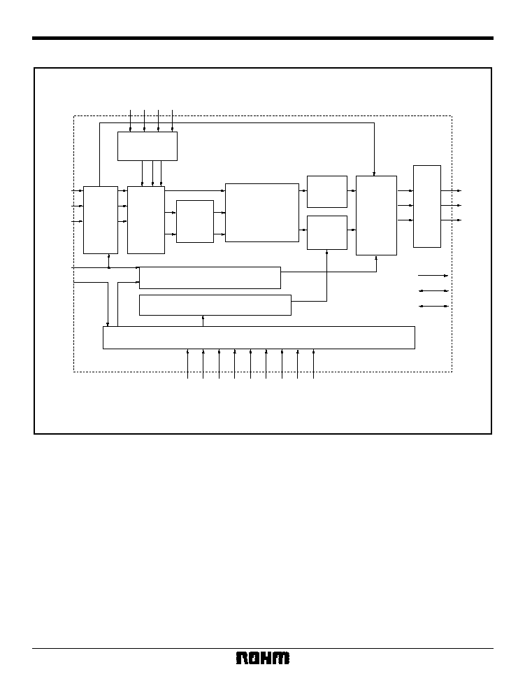
Block diagram
BOSD
GOSD
ROSD
OSDSW
OSD PALETTE
RGB 24BITS
Y-FILTER
MIX SIG
and
sync
burst
DAC
V
Y
C
C-FILTER
Y-LEVEL ADJ
CHROMA GEN
UV
FILTER
LATCH
RD
GD / Y
BD / UV
VCLK
RSTB
VIDEO TIMING CONTROL
SYNC BLANK
BURST
SUB CARRIER BURST GENERATOR
MODE CONTROL FIELD / FLAME CONTROL
VOUT
YOUT
COUT
PIXCLK
HSY
VSY
RGB
to
YUV
TEST12
ADDH
INT
IM [0.1]
YFILONB [1.0]
CDGSWB
PAL60B
NTB
CLKSW
3
Multimedia ICs
BU1425AK / BU1425AKV
∑
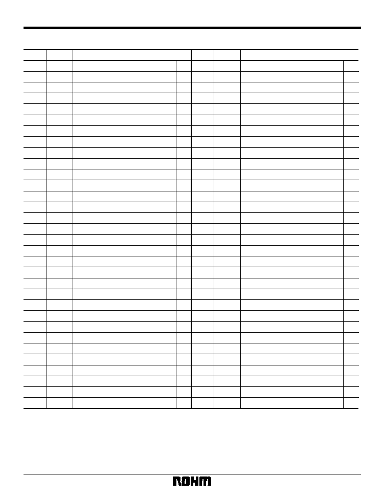
Pin descriptions
Pin No. Pin name
Function
1
2
3
4
5
6
7
8
9
10
11
12
13
14
15
16
17
18
19
20
21
22
23
24
25
26
27
28
29
30
31
32
With pull-down resistor (approx. 30k
)
BOSD
GD0 / Y0
GD1 / Y1
GD2 / Y2
GD3 / Y3
GD4 / Y4
GD5 / Y5
GD6 / Y6
GND
GD7 / Y7
BD0 / UV0
BD1 / UV1
BD2 / UV2
BD3 / UV3
OSDSW
CDGSWB
BD4 / UV4
BD5 / UV5
BD6 / UV6
BD7 / UV7
GND
NTB
IM0
IM1
TEST1
TEST2
VSY
HSY
PIXCLK
V
DD
IOV
DD
INT
33
34
35
36
37
38
39
40
41
42
43
44
45
46
47
48
49
50
51
52
53
54
55
56
57
58
59
60
61
62
63
64
SLABEB
ADDH
VREF-C
CGND
COUT
VGND
VOUT
AV
SS
P-V
DD
IR
AV
DD
YGND
YOUT
V
DD
YFILON2B
YCOFF
YFILON1B
PAL60B
VCLK
RSTB
CLKSW
RD0
RD1
RD2
ROSD
RD3
RD4
RD5
IOV
DD
RD6
RD7
GOSD
OSD BLUE DATA INPUT
GREEN DATA Bit0 (LSB)
GREEN DATA Bit1
GREEN DATA Bit2
GREEN DATA Bit3
GREEN DATA Bit4
GREEN DATA Bit5
GREEN DATA Bit6
DIGITAL GROUND
GREEN DATA Bit7 (MSB)
BLUE DATA Bit0 (LSB)
BLUE DATA Bit1
BLUE DATA Bit2
BLUE DATA Bit3
OSD ENABLE / DISABLE
SELECT Video-CD / CD-G
BLUE DATA Bit4
BLUE DATA Bit5
BLUE DATA Bit6
BLUE DATA Bit7 (MSB)
DIGITAL GROUND
SELECT NTSC / PAL MODE
SELECT YUV / RGB
SELECT DAC / NORMAL
Normally pull down to GND
SELECT U / V TIMING
V-SYNC INPUT or OUTPUT
H-SYNC INPUT or OUTPUT
1 / 2freq. of BCLK
DIGITAL V
DD
V
DD
for I / O
Interlace / Non-Interlace
Pin No. Pin name
SELECT MASTER / SLAVE
+ 0.5 / ≠
0.5LINE at NON-INTER
DAC BIAS
CHROMA OUTPUT GROUND
CHROMA OUTPUT
Composite Output Ground
COMPOSITE OUTPUT
Analog Ground (DAC VREF)
POWER (DAC) V
DD
REFERENCE RESISTOR
ANALOG (VREF) V
DD
Luminance Output Ground
Luminance Output
DIGITAL V
DD
Y-FILSEL THROU / FILON2
DAC (YOUTCOUT) OFF
Y-FILSEL THROU / FILON1
NORMAL / PAL60 at PALMODE
Video Clock Input
NORMAL / RESET
SEL
◊
1CLK /
◊
2CLK
RED DATA Bit0 (LSB)
RED DATA Bit1
RED DATA Bit2
OSD RED DATA INPUT
RED DATA Bit3
RED DATA Bit4
RED DATA Bit5
V
DD
for I / O
RED DATA Bit6
RED DATA Bit7
OSDGREEN DATA INPUT
Function

4
Multimedia ICs
BU1425AK / BU1425AKV
∑
Absolute maximum ratings (Ta = 25∞C)
Parameter
Symbol
Limits
Unit
Applied voltage
Input voltage
Storage temperature
Power dissipation
V
DD
, AV
DD
V
IN
Tstg
Pd
≠ 0.5 ~ + 7.0
≠ 0.3 ~ IOV
DD
+ 0.3
≠ 55 ~ + 150
1350
1
V
V
∞
C
mW
1
Reduced by 11mW for each increase in Ta of 1
∞
C over 25
∞
C.
1
When mounted on 120mm
◊
140mm
◊
1.0mm glass epoxy board.
Operation is not guaranteed at this value.
Not designed for radiation resistance.
∑
Recommended operating conditions
Parameter
Symbol
Limits
Unit
Power supply voltage
Power supply voltage
Input high level voltage
Input low level voltage
Analog input voltage
Operating temperature
V
DD
= AV
DD
IOV
DD
V
IH
V
IL
V
AIN
Topr
0 ~ + 0.8
0 ~ AV
DD
≠ 25 ~ + 60
4.50 ~
3.30 ~
2.1 ~
5.50
5.50
V
DD
V
V
V
V
V
∞
C
Should be used at V
DD
= AV
DD
.
∑
Electrical characteristics (unless otherwise noted, Ta = 25∞C, V
DD
= AV
DD
= 5.0V, GND = AV
SS
= VGND = CGND = YGND)
Parameter
Symbol
Min.
Typ.
Max.
Unit
Conditions
Digital block
Burst frequency 1
Burst frequency 2
Burst cycle
Operating circuit current 1
Operating circuit current 2
Output high level voltage
Output low level voltage
Input high level voltage
Input low level voltage
Input high level current
Input low level current
fBST1
fBST2
CBST
Idd1
Idd2
V
OH
V
OL
V
IH
V
IL
I
IH
I
IL
--
--
--
--
--
4.0
--
2.1
--
3.57954
4.43361
9
80
40
4.5
0.5
--
--
0.0
0.0
--
--
--
--
--
--
1.0
--
0.8
10.0
10.0
MHz
MHz
CYC
mA
mA
V
V
V
V
µ
A
µ
A
27MHz color bar
27MHz color bar PD mode
I
OH
= ≠ 2.0mA
I
OH
= 2.0mA
≠ 10
≠ 10
DAC block
DAC resolution
Linearity error
Y white level current
Y black level current
Y zero level current
V white level current
V black level current
V zero level current
RES
EL
IYW
IYB
IYZ
IYW
IYB
IYZ
--
--
--
--
--
--
9
25.14
7.24
0.0
25.14
7.24
0.0
--
--
--
10.0
--
--
10.0
BITS
LSB
mA
mA
µ
A
mA
mA
µ
A
IR = 1.2k
Sleep mode current
Iddpd
--
--
1.0
µ
A
V
IN
Max. = IOV
DD
+ 0.3V
V
IN
Min. = ≠ 0.3V
≠ 10
≠ 10
±
0.5
±
3.0

5
Multimedia ICs
BU1425AK / BU1425AKV
∑
Application example
(1) Example in Master mode: Doubled clock is input and 24-bit RGB input is used
1
2
3
4
5
6
7
8
9
10
11
12
13
14
15
16
48
47
46
45
44
43
42
41
40
39
38
37
36
35
34
33
17
18
19
20
21
22
23
24
25
26
27
28
29
30
31
32
7
6 5
4
3
2
1
0
3
7
6
5
4
6
7
4
3
5
1
0
2
2
1
0
B Data 0...7
G Data 0...7
R Data 0...7
[Blue]
[Green]
[Red]
OSD in
Vsync out
Hsync out
OSD CLOCK
75
75
75
OSD in
OSD in
Video-CD / CD-G
64
63
62
61
60
59
58
57
56
55
54
53
52
51
50
49
Reset [Low active] in
Pixel Clock in
Y-filter select
INTERLACE / NON-INTER
PAL / NTSC
DIGITAL GND
Chrominance
Composite
Luminance
MAIN V
DD
5.0 V
SLEEP MODE CTL
L: SLEEP
H: NORMAL
I / O V
DD
5.0V or 3.3V
BU1425AK / AKV
ANALOG V
DD
1.2k
0.01
µ
F
ANALOG GND
POWER GND
POWER V
DD
DIGITAL V
DD
CDGSWB
OSDSW
BD3
BD2
BD1
BD0
GD7
GND
GD6
GD5
GD4
GD3
GD2
GD1
GD0
BOSD
SLABEB
ADDH
VREF
CGND
COUT
VGND
V
OUT
AV
SS
AV
DD
IR
AV
DD
YGND
YOUT
V
DD
YFILON2B
YCOFF
BD4
BD5
BD6
BD7
GND
NTB
IM0
IM1
TEST1
TEST2
VSY
HSY
PIXCLK
V
DD
I / O V
DD
INT
GOSD
RD7
RD6
I / O V
DD
RD5
RD4
RD3
ROSD
RD2
RD1
RD0
CLKSW
RSTB
VCLK
PAL GOB
YFILON1B
OSD enable
Fig.1

6
Multimedia ICs
BU1425AK / BU1425AKV
(2) Example in Slave mode: Doubled clock is input and 16-bit YUV input is used
1
2
3
4
5
6
7
8
9
10
11
12
13
14
15
16
48
47
46
45
44
43
42
41
40
39
38
37
36
35
34
33
17
18
19
20
21
22
23
24
25
26
27
28
29
30
31
32
7
6 5
4
3
2
1
0
3
7
6
5
4
6
7
4
3
5
1
0
2
2
1
0
U.V Data 0...7
Y Data 0...7
[Blue]
[Green]
[Red]
OSD in
OSD CLOCK
75
75
75
OSD in
OSD in
Video-CD / CD-G
64
63
62
61
60
59
58
57
56
55
54
53
52
51
50
49
Reset [Low active] in
Pixel Clock in
Y-filter select
INTERLACE / NON-INTER
PAL / NTSC
DIGITAL GND
Hsync in
Vsync in
Chrominance
Composite
Luminance
MAIN V
DD
5.0V
SLEEP MODE CTL
L: SLEEP
H: NORMAL
I / 0 V
DD
5.0V or 3.3V
BU1425AK / AKV
ANALOG VDD
0.01
µ
F
ANALOG GND
POWER GND
POWER VDD
DIGITAL VDD
CDGSWB
OSDSW
BD3
BD2
BD1
BD0
GD7
GND
GD6
GD5
GD4
GD3
GD2
GD1
GD0
BOSD
SLABEB
ADDH
VREF
CGND
COUT
VGND
V
OUT
AV
SS
AV
DD
IR
AV
DD
YGND
YOUT
V
DD
YFILON2B
YCOFF
BD4
BD5
BD6
BD7
GND
NTB
IM0
IM1
TEST1
TEST2
VSY
HSY
PIXCLK
V
DD
I / O V
DD
INT
GOSD
RD7
RD6
I / O V
DD
RD5
RD4
RD3
ROSD
RD2
RD1
RD0
CLKSW
RSTB
YCLK
PAL GOB
YFILON1B
1.2k
Fig.2
OSD enable
7
Multimedia ICs
BU1425AK / BU1425AKV
∑
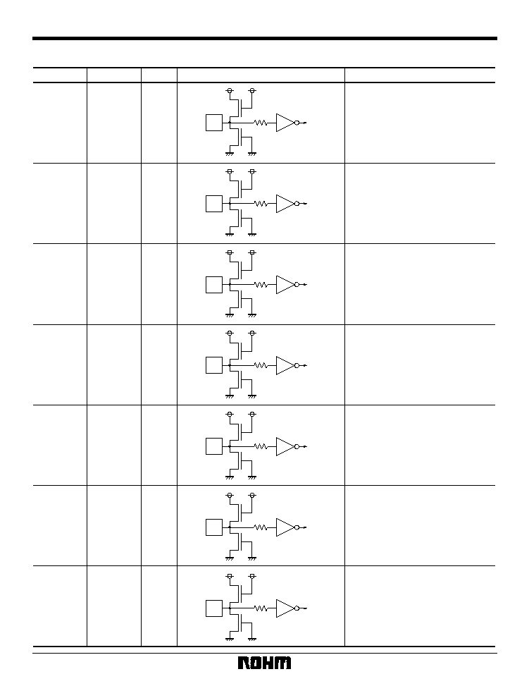
Equivalent circuits
Pin No.
Pin name
Equivalent circuit
I / O
Function
2 ~ 8
10
GD (7: 0)
G data input pin for 24-bit RGB input
Y data input pin for 16-bit YUV input
11 ~ 14
17 ~ 20
BD (0: 7)
B data input pin for 24-bit RGB input
U, V data input pins for 16-bit YUV
input
Control pins used to select RGB (24-
bit), YUV (16-bit) or DAC Through as
the input mode.
16
CDGSWB
Switches the mode between Video-
CD (HIGH) and CD-G (LOW).
54 ~ 56
58 ~ 60
62.63
RD (0: 7)
R data input pin for 24-bit RGB input
1
57
64
15
ROSD
GOSD
BOSD
OSDSW
OSD data input pin when using the
OSD function.
When the OSDSW pin is HIGH, input
to the ROSD, GOSD, and BOSD pins
takes precedence over RGB, and the
data is converted.
23
24
IM0
IM1
22
NTB
Switches the mode between NTSC
(LOW) and PAL (HIGH).
I
I
I
I
I
I
I

8
Multimedia ICs
BU1425AK / BU1425AKV
Pin No.
Pin name
Equivalent circuit
I / O
Function
27
VSY
I / O
Vertical synchronization signals (Vsync)
are input (when SLABEB = LOW) or
output (when SLABEB = HIGH) here.
35
VREF-C
I
This is the reference voltage generator
circuit monitoring pin which deter-
mines the output amplitude (output cur-
rent for 1 LSB) of the DAC. A 0.01
µ
F
capacitor should be attached between
this and pin 43 (AV
DD
).
29
PIXCLK
O
The internal processing clock is divid-
ed in half and output. Data is read at
the point at which the edge of this
clock changes. This can also be used
as the clock for the OSD IC.
32
INT
I
This pin switches between interlace
(when HIGH) and non-interlace (when
LOW) modes. This pin is effective in
both the VIDEO-CD and CD-G
modes.
33
34
SLABEB
ADDH
I
I
This pin switches between the Master
(when HIGH) and Slave (when LOW)
modes. It is effective in the non-
interlace mode, and it switches bet-
ween ≠ 0.5 lines (when LOW) and + 0.5
lines (when HIGH) for the number of
lines in an interlace field.
28
HSY
I / O
This is the horizontal synchronization
signal pin. Negative polarity Hsync
signals are input (when SLABEB =
LOW) or output (when SLABEB =
HIGH) here. This is also used as the
synchronization signal for fixing the
PIXCLK output phase.
37
COUT
O
This is the chrominance output pin for
the S pin.

9
Multimedia ICs
BU1425AK / BU1425AKV
Pin No.
Pin name
Equivalent circuit
I / O
Function
39
VOUT
O
Composite output pin
45
YOUT
O
Luminance output pin for the S pin
42
IR
I
The output amplitude (output current
for 1 LSB) of the DAC is specified
using an external resistor, and this pin
controls the value of the current flow-
ing per bit.
48
YCOFF
I
When there is HIGH input at the signal
input pin which switches to and from
the low power consumption mode, this
turns off the output from the YOUT
and COUT pins.
51
49
VCLK
Input pin for the reference clock in the
Video-CD mode
52
RSTB
Reset input pin which initializes the
system. The system is reset when
this goes LOW.
YFILON1B
YFILON2B
Selects the F characteristic of the
Y-FILTER.
I
I
I

10
Multimedia ICs
BU1425AK / BU1425AKV
Pin No.
Pin name
Equivalent circuit
I / O
Function
53
CLKSW
I
50
PAL60B
Switches between the PAL and PAL60
modes. This is effective only when
the NTB pin is HIGH. (PAL mode
only)
This switches between dividing the
VCLK input in half and using it as an
internal clock (when LOW), and using
it as an internal clock without dividing
it in half (when HIGH).
25
26
TEST1
TEST2
I
Normally, this is connected to the
GND pin. However, when 16-bit YUV
input is used, the TEST2 pin can be
used as the U and V timing control
pins.
I
31
46
61
41
43
AV
DD
IOV
DD
Power supply pin for the digital, the
analog, and I / O blocks
9
21
36
38
40
44
GND
CGND
VGND
AV
SS
YGND
Grounding pin for the digital and
analog blocks
30
V
DD
Digital V
DD
. Equipped with pull-down
resistor.

11
Multimedia ICs
BU1425AK / BU1425AKV
∑
Circuit operation
Table 1: Low power consumption mode with the YCOFF pin
Pin No.
Pin Name
YCOFF
LOW
HIGH
VOUT pin
Composite signal
Composite signal
48
Output Mode and Power Consumption
YOUT pin
Luminance signal
No output (0V)
COUT pin
Chrominance signal
No output (0V)
Power consumption (typ.)
0.45W
0.25W
(1) Overview
The BU1425AK / AKV converts digital images and video
data with an 8-bit configuration to 9-bit composite signals
(V
OUT
), luminance signals (YOUT), and chrominance sig-
nals (COUT) for the NTSC, PAL, and PAL60 formats,
and outputs the converted data as analog TV signals.
The user may select whether V
OUT
consists of chromi-
nance signals that have passed through a chrominance
band pass and luminance signals that have been mixed,
or luminance signals that have passed through a chromi-
nance trap and luminance signals that have not passed
through a chrominance trap. The F characteristic of this
chrominance trap may be selected from among three
available types. Since YOUT normally does not pass
through the trap, it is optimum for the S pin. COUT nor-
mally passes through the chrominance band pass, and is
thus highly resistance to dot interference. In addition,
when used in the doubled clock mode, it passes through
an interpolator filter, and for that reason is able to repro-
duce even cleaner image quality.
A correspondence can be set up between input digital
image data and Video-CD and CD-G decoder output.
Output TV signals, in addition to switching among the
NTSC, PAL, and PAL60 modes, can be switched
between the interlace and non-interlace modes.
The data clock input to the VCLK pin can also be input as
a doubled clock for the data rate (in doubled clock
modes). In doubled clock modes, data is read and
processed at the rising edge of an internal clock that has
been divided in half. In ordinary clock modes, data is
read and processed at the rising edge of the clock that
has the same phase as the input clock. Two input data
formats are supported: 24-bit RGB (4: 4: 4) and 16-bit
YUV (4: 2: 2). These are input to RD0 to 7, GD0 to 7, and
BD0 to 7, respectively. The selected input format can be
switched using the IM0 and IM1 pin input. When the
OSDSW pin is set to the "Enabled" (H) state, data input
to the ROSD, GOSD, and BOSD pins becomes effective,
making it possible to input 7-color (8 including black)
chrominance data. At the same time, a clock with a fre-
quency half that of the internal clock is output from the
PIXCLK pin. As a result, the PIXCLK pin can easily be
directly connected to the OSD IC clock input pin, and the
OSDSW pin can be directly connected to the BLK output
pin. Thus, the BU1425AK and the OSD IC can be syn-
chronized, and OSD text with a burster trimmer stacker
feature can be used.
If the input data is in the RGB format, it is converted to
YUV. If it is in the YUV format, it is converted from the
CCIR-601 format to level-shifted YUV data. The YUV
data is then adjusted to the 100IRE level in the NTSC,
PAL, and PAL60 modes, and U and V data is phase-
adjusted by a sub-carrier generated internally, and is
modulated to chrominance signals.
Ultimately, elements such as the necessary synchroniza-
tion level, the color blanking level, and burst signals are
mixed, and pass through the 9-bit DAC to be output as
NTSC or PAL composite signals, luminance signals, and
chrominance signals (conforming to RS-170A). At this
point, the DAC is operating at twice the internal clock,
making it possible to reduce the number of attachments.
Furthermore, luminance signal output and chrominance
signal output can be turned off. At this point, it is possible
to reduce the level of power consumption.
The DAC output is current output. If a resistor of a speci-
fied value is connected to the IR pin, 2.0V
P-P
output can
be obtained by connecting 75
to the VOUT pin as an
external resistor. As a result, normally, when a video
input pin (75
terminus) is connected, the output is
approximately 1.0V
P-P
voltage output at a white 100%
level.
(2) Specifying the mode
1) Power saving mode
With the BU1425AK / AKV, setting the YCOFF pin to
HIGH turns off the output from the YOUT and COUT pins
of the DAC output, enabling use in the low power con-
sumption mode.

12
Multimedia ICs
BU1425AK / BU1425AKV
2) Output modes
The "Video-CD" and "CD-G" modes can be supported
by both digital image and video data, with the mode
being switched by the CDGSWB pin input. When the
CDGSWB pin input is LOW, the CD-G mode is set, and
when HIGH, the Video-CD mode is set. Also, the
"NTSC", "PAL", and "PAL60" modes may be selected
as the output TV modes. The output TV mode is
switched using the NTB and PAL60 pin input. Setting
the NTB pin input to LOW sets the NTSC mode, and
setting it HIGH with the PAL60 pin also HIGH sets the
PAL mode. Setting the NTB pin HIGH and the PAL60
pin LOW, sets the PAL60 mode.
Table 2: Specifying modes
NTB
PAL60
0
0
1
1
CDGSWB
0
1
0
1
0
1
Decoder mode
CD-G
Video-CD
CD-G
Video-CD
CD-G
Video-CD
0
0
1
1
1
1
TV mode
NTSC
NTSC
PAL60
PAL60
PAL
PAL
Also, INT pin input can be used to switch between
"interlace output" and "non-interlace output."
Setting the input to LOW enables non-interlace output,
and setting it to HIGH enables interlace output. When
non-interlace output is used, the number of lines in one
field can be controlled using the ADDH pin. If the ADDH
pin is LOW, the number of lines in one field is set to the
number of interlace output lines minus 0.5 lines, and
when HIGH, the number of lines in one field is set to the
number of interlace output lines plus 0.5 lines.
Table 3: Pin settings for interlace / non-interlace modes
INT
A
DD
H
Scan Mode
No. of Lines / Field
0
1
Non-interlace
Non-interlace
Interlace
262
263
262.5
312
313
312.5
0
0
1
NTSC / PAL60
PAL
3) Input formats
The digital data input format can be set as shown in the
table below, using the IM1 and IM0 pins. Both 24-bit
RGB (4: 4: 4) and 16-bit YUV (4: 2: 2) are supported. In
addition, digital RGB input can be output as analog
RGB output (RGB Through mode).
Table 4: Input format settings
IM1
IM0
0
1
0
1
Input format
R (8 bits), G (8 bits), B (8 bits)
16-bit YUV (4: 2: 2)
--
ROSD, GOSD, BOSD expanded to RGB input
Output signal
TV signals (9-bit resolution)
TV signals (9-bit resolution)
--
RGB analog signals (9 bits)
0
0
1
1
13
Multimedia ICs
BU1425AK / BU1425AKV
Table 5: Bit assignments in RGB Through mode
Output Pin
YOUT (45)
VOUT (39)
COUT (37)
BIT8
RD7
GD7
BD7
BIT7
RD6
GD6
BD6
BIT6
RD5
GD5
BD5
BIT5
RD4
GD4
BD4
BIT4
RD3
GD3
BD3
BIT3
RD2
GD2
BD2
BIT2
RD1
GD1
BD1
BIT1
RD0
GD0
BD0
BIT0
ROSD
GOSD
BOSD
The BU1425AK / AKV has an internal OSD switch and
chrominance data generating function. Consequently,
joint usage of an OSD-IC with blanking and R, G, and B
output can be easily supported by the OSD. Moreover,
a clock with half the internal processing frequency of
the BU1425AK is output from the PIXCLK pin, and can
be connected to the OSD-IC clock input, enabling the
timing to be captured.
ROSD, GOSD, and BOSD pin input is effective as long
as the OSDSW pin input is HIGH. The relationship
between OSD data and chrominance data is as shown
in Table 6 below.
Table 6: Correspondence between OSD function, input data and chrominance output
OSDSW
ROSD
0
0
0
0
1
1
1
1
GOSD
0
0
1
1
0
0
1
1
BOSD
0
1
0
1
0
1
0
1
1
1
1
1
1
1
1
1
0
Output Chrominance Signal
Black (blanking)
Blue
Green
Cyan
Red
Magenta
Yellow
White
Based on input specified by IM0 and IM1
4) Clock modes
With the BU1425AK / AKV, clock input is available at the
VCLK pin.
Clocks supplied from an external source should basically
be input at a frequency double that of clocks used inter-
nally (basic clock: BCLK) (when the CLKSW pin is LOW).
The phase relationship between the internal clock and
the external clock at this time is as shown in Fig. 3, with
the HSY pin input serving as a reference. In the Master
mode, in which data from the HSY pin is output and
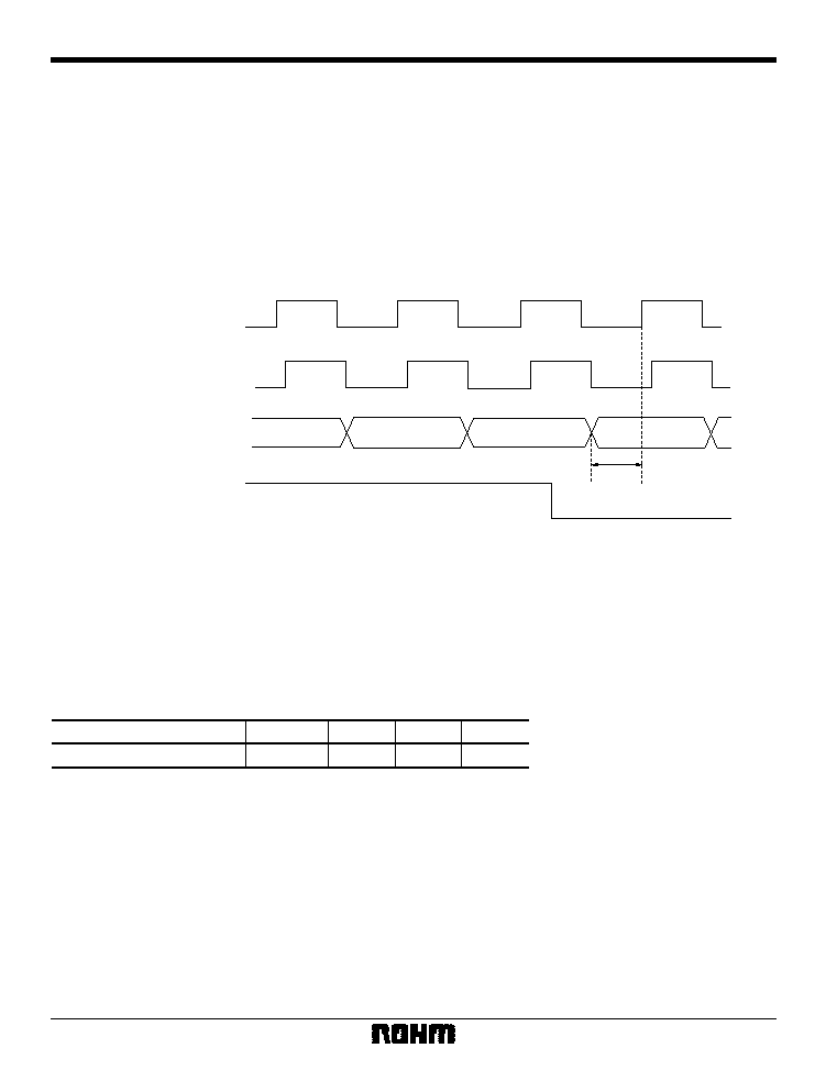
used, HSY is output at the timing shown in Fig. 3. With
the BU1425AK, data (RD, GD, BD, etc.) is read at the ris-
ing edge of the internal clock (BCLK), so data should be
input to the BU1425AK / AKV as shown in Fig. 3.
HSY
VCLK
Internal clock (BCLK)
Input data
Fig. 3 Illustration of clock timing (CLKSW is LOW)

14
Multimedia ICs
BU1425AK / BU1425AKV
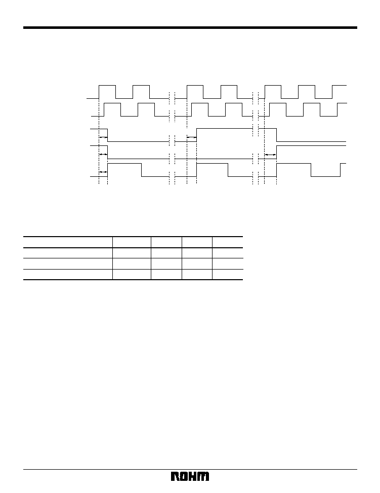
Also, setting the CLKSW pin to HIGH enables the fre-
quency of the external clock to be used as BCLK, the
internal clock, just as it is. Since the data is read to the
BU1425AK / AKV at the rising edge of BCLK at this
time as well, data should be input as shown in Fig. 4.
The relationship with HSY is also as shown in Fig. 4.
HSY
VCLK
Internal clock (BCLK)
Input data
Fig. 4 Illustration of clock timing (CLKSW is HIGH)
With the BU1425AK / AKV, the sub-carrier (burst) fre-
quency is generated using the internal clock. For this
reason, the frequencies used in the various modes are
limited, so those frequencies should be input (see Table
7 below).
Table 7: BU1425AK / AKV clock input frequency settings
CLKSW Pin
Video-CD Mode
27.000MHz
13.500MHz
CD-G Mode
Same for NTSC / PAL / PAL60
NTSC
28.636MHz
14.318MHz
0
1
PAL / PAL60
28.3750MHz
14.1875MHz
5) Synchronization signals
The BU1425AK / AKV has an "Encoder Master" mode in
which synchronization signals are output, and an
"Encoder Slave" mode in which synchronization signals
are input from an external source and used to achieve
synchronization. These modes are switched at the
SLABEB pin. When the SLABEB pin is LOW, the Slave
mode is in effect, and when HIGH, the Master mode is in
effect.
In the Master mode, the HSY and VSY pins serve as out-
put, with horizontal synchronization signals (HSYNC)
being output from the HSY pin and vertical synchroniza-
tion signals (VSYNC) from the VSY pin. At this time, the
reference timing for synchronization signal output is
determined at the rising edge of the RSTB pin. Output is
obtained in accordance with the specified mode (NTSC,
PAL, or PAL60, interlace or non-interlace). Output in the
non-interlace mode, however, is output only under "Odd"
field conditions (the falling edges of Hsy and Vsy are the
same).
In the Slave mode, the HSY and VSY pins serve as input,
and horizontal synchronization signals (HSYNC) should
be input to the HSY pin and vertical synchronization sig-
nals (VSYNC) to the VSY pin. The input synchronization
signals at this time should be input in accordance with
the specified mode. With the BU1425AK / AKV, field dis-
tinction between odd and even fields is made automati-
cally for each field when interlace input is used. With the
BU1425AK, all synchronization signals are treated as
negative polarity signals (signals for which the sync inter-
val goes LOW). When using the non-interlace mode,
operation is normally carried out under odd field condi-
tions (the falling edges of Hsy and Vsy are simultane-
ous).

15
Multimedia ICs
BU1425AK / BU1425AKV
6) Y filter
With the BU1425AK / AKV, the frequency characteristic
of Y, which is mixed with the VOUT pin output, is set so
that it can be selected using the YFILON1B and 2B pins.
A through filter is normally used on the YOUT pin output,
so that it is not limited to this method.
Table 8: Frequency characteristic of the Y channel
YFILON2B
YFILON1B
H
TRAP filter through
(same signal as YOUT pin output is mixed with VOUT)
Frequency characteristic of the Y channel
chart1
chart2
chart3
H
H
L
L
L
H
L
100
≠ 40
10
20000
10000
1000
AMPLITUDE (dB)
PHASE (deg)
FREQUENCY (kHz)
5
0
≠ 5
≠ 10
≠ 15
≠ 20
≠ 25
≠ 30
≠ 35
90
45
0
180
135
≠ 45
≠ 90
≠ 135
≠ 180
Gain-Phase Graphic
Fig.5 chart1 (BCLK = 13.5MHz)
100
≠ 40
10
20000
10000
1000
AMPLITUDE (dB)
FREQUENCY (kHz)
5
0
≠ 5
≠ 10
≠ 15
≠ 20
≠ 25
≠ 30
≠ 35
PHASE (deg)
90
45
0
180
135
≠ 45
≠ 90
≠ 135
≠ 180
Gain-Phase Graphic
Fig.6 chart2 (BCLK = 13.5MHz)
100
≠ 40
10
20000
10000
1000
AMPLITUDE (dB)
FREQUENCY (kHz)
5
0
≠ 5
≠ 10
≠ 15
≠ 20
≠ 25
≠ 30
≠ 35
PHASE (deg)
90
45
0
180
135
≠ 45
≠ 90
≠ 135
≠ 180
Gain-Phase Graphic
Fig.7 chart3 (BCLK = 14.318MHz)

16
Multimedia ICs
BU1425AK / BU1425AKV
(3) Output level
Figures 8 to 10 indicate the digital data values for the
DAC output when the color bars from the various pins
are reproduced.
WHITE
YELLOW
CYAN
GREEN
MAGEN
RED
BLUE
BLACK
BLACK LEVEL
= PEDESTAL LEVEL
SYNC TIP LEVEL
Fig. 8 YOUT output
B
L
A
C
K
W
H
I
T
E
Y
E
L
L
O
W
C
Y
A
N
G
R
E
E
N
M
A
G
E
N
T
A
R
E
D
B
L
U
E
COLOR
BURST
BLACK LEVEL
Fig. 9 COUT output
BLACK LEVEL
= PEDESTAL LEVEL
SYNC TIP LEVEL
Y
E
L
L
O
W
C
Y
A
N
G
R
E
E
N
M
A
G
E
N
T
A
R
E
D
B
L
U
E
B
L
A
C
K
W
H
I
T
E
Fig. 10 VOUT output

17
Multimedia ICs
BU1425AK / BU1425AKV
Table 9: BU1425AK color bar input / output data
RD
--
--
--
--
00
00
00
00
FF
FF
FF
FF
SYNC TIP
Color Burst NTSC
Color Burst PAL
BLANK LEVEL
BLACK (Pedestal)
BLUE
GREEN
CYAN
RED
MAGENTA
YELLOW
WHITE
RGB24bit
YOUT
GD
--
--
--
--
00
00
FF
FF
00
00
FF
FF
BD
--
--
--
--
00
FF
00
FF
00
FF
00
FF
YD
--
--
--
--
10
28
90
A9
51
6A
D2
EB
YUV (4: 2: 2)
NAME&COLOR
UD
--
--
--
--
80
F1
36
A5
5A
C9
0E
80
Input (8-bit hexadecimal for each)
Output (9-bit hexadecimal for each)
VD
--
--
--
--
80
6D
22
10
F0
DD
92
80
±
033
±
038
±
072
±
096
±
0A0
±
0A0
±
096
±
072
±
033
±
038
±
072
±
096
±
0A0
±
0A0
±
096
±
072
000
--
--
--
072
092
117
138
0C6
0E6
16C
18C
COUT
V
OUT
COUT and VOUT display the chrominance amplitude. COUT is C8H
±
XXXH.
VOUT is YOUT
±
XXXH.
--
--
000
000
100
072
000
000
(4) Timing
Table 10 below shows the input and output pins related
to timing.
Table 10: BU1425AK timing-related input / output pins
Pin No.
Pin name
Function
52
51
53
27
28
16
22
50
32
33
34
29
RSTB
VCLK
CLKSW
VSY
HSY
CDGSWB
NTB
PAL60B
INT
SLABEB
ADDH
PIXCLK
I / O
I
I
I
I / O
I / O
I
I
I
I
I
I
O
System reset input pin
Clock input pin
Clock input mode setting pin
Vertical synchronization signal I / O pin
Horizontal synchronization signal I / O pin
Video-CD / CD-G mode switching pin
NTSC / PAL mode switching pin
PAL / PAL60 mode switching pin
Interlace / Non-interlace mode switching pin
Master / Slave mode switching pin
Pin which adds 1 line in non-interlace mode
1 / 2 divider output for internal clock (OSD clock)
18
Multimedia ICs
BU1425AK / BU1425AKV
1) Input clocks and input data timings in the various
operation modes
There are slight differences in the input data and the clock
timing, depending on which mode is being used. What is
shared by all modes is that, with the BU1425AK / AKV,
data is read and discharged at the rising edge of the
internal clock. The illustration below shows the input con-
ditions in the various modes.
1. Master mode,
1 clock mode
Encoder master (pin 33 = H)
Internal clock = input clock (pin 53 = H)
Input data
Output data (HSY, VSY)
VCLK (pin53)
Tds1
Internal clock (BCLK)
Fig.11
In this mode, the internal clock (BCLK) begins to operate at the same phase as the VCLK input, following the rise
of the RSTB pin (pin 52).
Table 11
Parameter
Symbol
Max.
Typ.
Min.
Tds1
--
--
10
Data setup time 1

19
Multimedia ICs
BU1425AK / BU1425AKV
2. Master mode, doubled clock mode
Encoder master (pin 33 = H)
Internal clock = 2
input clock (pin 53 = H)
Input data
Output data
(HSY, VSY)
VCLK (pin53)
Tds2
Internal clock
(BCLK)
Fig.12
In this mode, the internal clock (BCLK) begins to operate at a halved frequency at the rise of the VCLK input, fol-
lowing the rise of the RSTB pin (pin 52).
Table 12
Parameter
Symbol
Max.
Typ.
Min.
Tds2
--
--
10
Data setup time 2
3. Slave mode,
1 clock mode
Encoder slave (pin 33 = H)
Internal clock = input clock (pin 53 = H)
Input data
Input data
(HSY, VSY)
VCLK (pin53)
Tds3S
Internal clock
(BCLK)
Tds3H
Tsh1
Tsd1
Fig.13

20
Multimedia ICs
BU1425AK / BU1425AKV
In this mode, the internal clock (BCLK) begins to operate at the same phase as the VCLK input, following the rise
of the RSTB pin (pin 52).
Table 13
Parameter
Symbol
Max.
Typ.
Min.
Tds3S
Tds3H
Tsd1
Tsh1
--
--
--
--
--
--
--
--
5
8
5
8
Data setup time 3S
Data hold time 3H
Sync signal setup time
Sync signal hold time
4. Slave mode, doubled clock mode
Encoder slave (pin 33 = L)
Internal clock = 2
input clock (pin 53 = L)
Tsh2
Tsd2
Input data
Input data
(HSY, VSY)
VCLK (pin53)
Tds4
Internal clock
(BCLK)
Fig.14
In this mode, the internal clock (BCLK) begins to operate at a halved frequency at the rise of the VCLK input, fol-
lowing the rise of the RSTB pin (pin 52). When HSY is input, phase correction is carried out at the falling edge, as
shown in Fig. 14. (In other words, the phase of the internal clock (BCLK) is not determined until HSY is input.)
Table 14
Parameter
Symbol
Max.
Typ.
Min.
Tds4
Tsh2
Tsd2
--
--
--
--
--
--
10
10
10
Data setup time 4
Sync signal hold time 2
Sync signal setup time 2

21
Multimedia ICs
BU1425AK / BU1425AKV
2) Clock timing when the OSD function is used
Eight-color OSD color with a burster trimmer stacker fea-
ture can be used, simply by connecting an OSD with
external clock input. Output from the PIXCLK pin of the
BU1425AK should be input to the OSC-IN of the OSD IC.
The OSDSW input pin can be used as a signal for the
burster trimmer stacker feature called VBLK, or a similar
name. (See page 13 for a table showing the correspon-
dence between input data and color output.)
BLACK
YELLOW
VIDEO-DATA
VIDEO-DATA
Internal clock (BCLK)
HSY (IN / OUT)
PIXCLK
OSDSW
ROSD.GOSD
V.Y.C.OUT
Fig. 15 Clock timing with the OSD function
The frequency of the PIXCLK pin output is one-half that of the internal clock. This phase is determined at the rising
edge of HSY, as shown in Fig.15. (In the Encoder Master mode, phase correction is implemented using the HSY
output of the BU1425AK itself.) The OSD function is effective only during the time that video output is enabled.
(See the TV signal timing diagram on page 27.)

22
Multimedia ICs
BU1425AK / BU1425AKV
3) Output timing
1. Master mode, doubled clock mode
Encoder master (pin 33 = H)
Internal clock = input clock
1 / 2 (pin 53 = L)
Thdf
Tvdf
Tpdr
VCLK
Internal clock (BCLK)
HSY (OUT)
VSY (OUT)
PIXCLK (OUT)
Thdr
Tvdr
Fig. 16 Output timing with a doubled clock
Table 15
Parameter
Symbol
Max.
Typ.
Min.
Thdr Thdf
Tvdr Tvdf
Tpdr Tpdf
--
--
--
14
14
14
--
--
--
HSY output delay
VSY output delay
PIXCLK output delay
23
Multimedia ICs
BU1425AK / BU1425AKV
2. Master mode, regular clock mode
Encoder master (pin 33 = H)
Internal clock = input clock (pin 53 = L)
Thdf
Tvdf
Tpdr
VCLK
Internal clock (BCLK)
HSY (OUT)
VSY (OUT)
PIXCLK (OUT)
Tvdr
Thdr
Fig. 17 Output timing with a clock at the regular frequency
Table 16
Parameter
Symbol
Max.
Typ.
Min.
Thdr Thdf
Tvdr Tvdf
Tpdr Tpdf
--
--
--
10
10
10
--
--
--
HSY output delay
VSY output delay
PIXCLK output delay

24
Multimedia ICs
BU1425AK / BU1425AKV
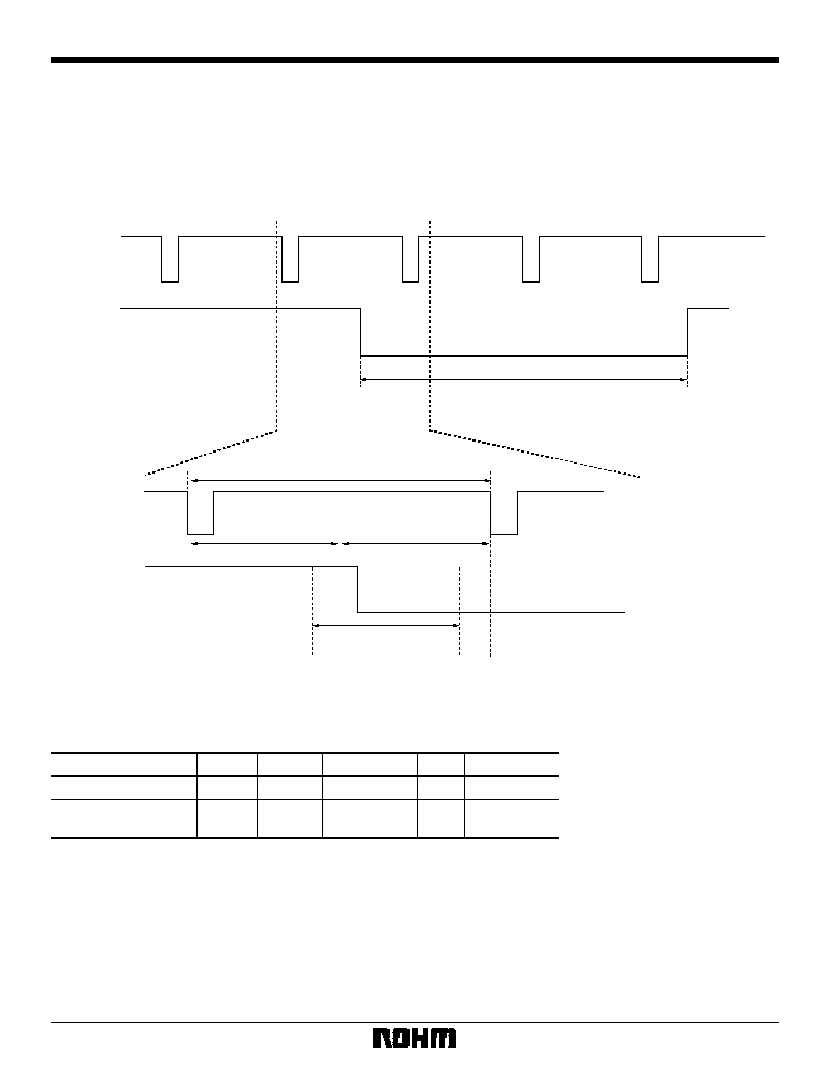
4) Odd / even recognition timing in Slave mode
1. Timing based on recognition of odd conditions
The BU1425AK / AKV distinguishes whether the condi-
tions of each field (each time that VSY is input) are odd
or otherwise, and internal operation is carried out based
on that recognition after the data is input. As a result,
HSY and VSY are input under input conditions appropri-
ate to the specified mode, enabling regulated output for
the first time. Odd input conditions are indicated below.
Timing that does not match these conditions is recog-
nized as an even field.
Expanded view
HSY
VSY
HSY
Tvl
VSY
Thvdiff
Fig. 18 Odd recognition conditions
Table 17: Odd recognition conditions
VSY Delay from HSY
Parameter
Symbol
Max.
Typ.
Min.
Tvl
--
--
128
VSY input L interval
Thvdiff
Unit
BCLK
BCLK
HSY Rising edge
≠ 2clk
--
HSY falling edge
≠ 1clk
BCLK = One cycle of internal clock
25
Multimedia ICs
BU1425AK / BU1425AKV
2. Even timing
The BU1425AK / AKV distinguishes whether the condi-
tions of each field (each time that VSY is input) are odd
or otherwise, and internal operation is carried out based
on that recognition after the data is input. As a result,
HSY and VSY are input under input conditions appropri-
ate to the specified mode, enabling regulated output for
the first time. Timing that does not match the odd field
conditions is recognized as an even field. In order to pre-
vent malfunctioning of the internal HSY counter, howev-
er, there are regulations which apply to the timing at
which VSYNC is input in even fields.
Expanded view
HSY
VSY
HSY
T = 1 / Fhsync
T = 1 / Fhsync
1 / 2
T = 1 / Fhsync
1 / 2
The middle of HSY
Tvl
VSY
Thvdiff
Fig. 19 Even conditions
Table 18: Even conditions
Parameter
Symbol
Max.
Typ.
Min.
Tvl
--
--
128
VSY input L interval
Thvdiff
Unit
BCLK
BCLK
HSY Falling edge
≠ 128clk
--
The middle of HYS
≠ 128clk
VSY Delay from The
middle of HSY
BCLK = One cycle of internal clock
26
Multimedia ICs
BU1425AK / BU1425AKV
Parameter
Symbol
Unit
NTSC
V-CD
PAL
Td1
Td2
Td3
Td4
Td5
BCLK
BCLK
BCLK
BCLK
BCLK
SYNC rise
Burst start
Burst end
Data start
1-line interval
PAL60
CD-G
V-CD
CDG1
V-CD
CDG1
64
71
106
128
858
67
76
112
135
910
64
71
106
142
864
67
75
112
149
908
64
71
106
128
858
67
75
112
135
902
BURST
VOUT
(39)
BURST
BURST
BURST
YOUT
(45)
COUT
(37)
Td1
Td2
Td3
Td4
Td5
Fig. 20 TV signal timing diagram
Table 19
27
Multimedia ICs
BU1425AK / BU1425AKV
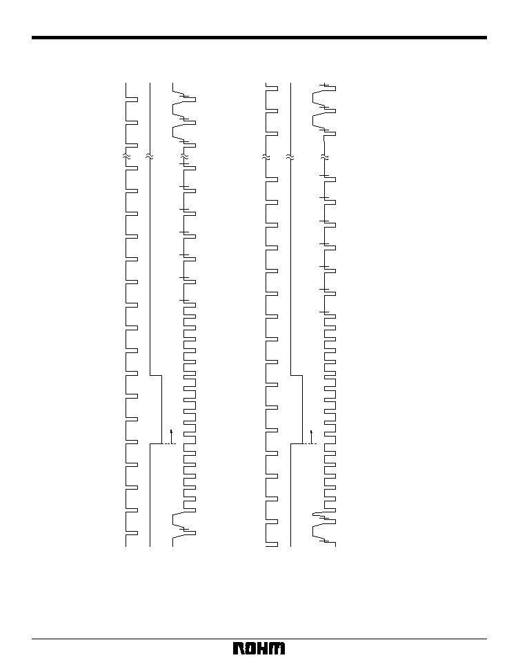
Frame timing in Video-CD mode
(NTSC / PAL60: Interlace)
522
523
524
525
Odd_Field
Hsync (28pin)
Vsync (27pin)
VOUT
(39pin)
123456789
1
0
1
1
1
2
1
8
1
9
2
0
Indicates a line interval during which video data is output
259
260
261
262
Even_Field
Hsync (28pin)
Vsync (27pin)
VOUT
(39pin)
263
264
265
266
267
268
269
270
271
272
273
274
281
282
Fig. 21
28
Multimedia ICs
BU1425AK / BU1425AKV
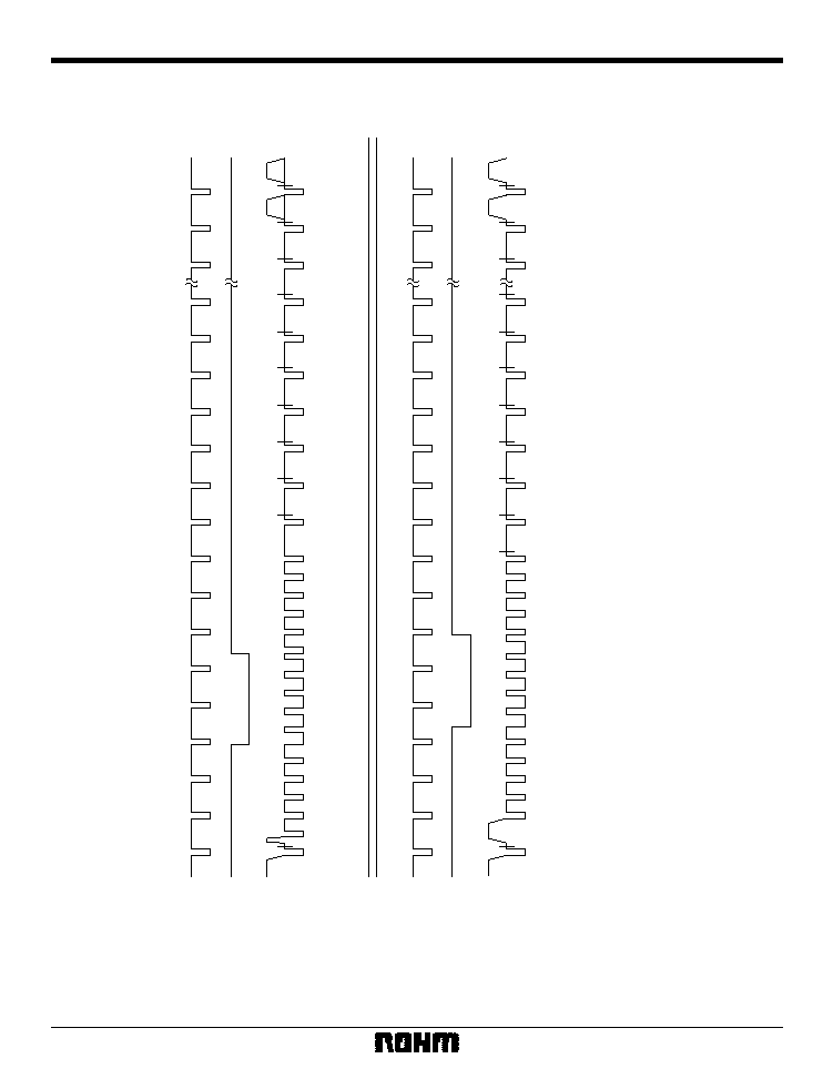
Frame timing in Video-CD mode
(PAL: Interlace)
Odd_Field
4
Hsync (28pin)
Vsync (27pin)
VOUT (39pin)
6
2
3
6
2
4
6
2
5
123456789
1
0
1
1
1
2
2
3
2
4
2
5
3
Even_Field
4
Hsync (28pin)
Vsync (27pin)
VOUT (39pin)
310
311
312
313
314
315
316
317
318
319
320
321
322
323
324
335
336
337
Fig.22
3 Indicates a line interval during which video data is output
4 First and second have been added to aid in explanation, but there is no actual distinction.

29
Multimedia ICs
BU1425AK / BU1425AKV
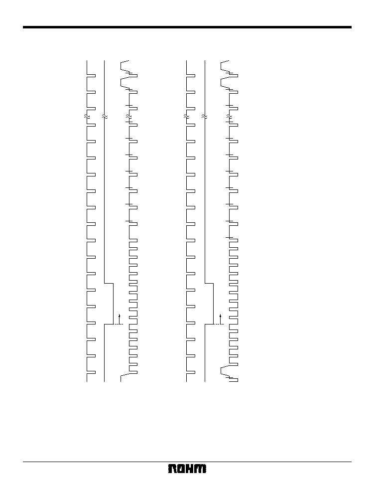
Frame timing in CD-G mode
(NTSC / PAL60: Non-interlace)
521
522
523
524
First_Field
4
Hsync (28pin)
Vsync (27pin)
VOUT
(39pin)
123456789
1
0
1
1
1
2
1
8
1
9
2
0
3
3 Indicates a line interval during which video data is output
4 First and second have been added to aid in explanation, but there is no actual distinction.
259
260
261
262
Second_Field
4
Hsync (28pin)
Vsync (27pin)
VOUT
(39pin)
263
264
265
266
267
268
269
270
271
272
273
274
281
282
Fig.23
30
Multimedia ICs
BU1425AK / BU1425AKV
Frame timing in CD-G mode
(PAL: Non-interlace)
Hsync (28pin)
Vsync (27pin)
VOUT
(39pin)
6
2
2
6
2
3
6
2
4
123456789
1
0
1
1
1
2
2
3
2
4
2
5
3
3 Indicates a line interval during which video data is output
4 First and second have been added to aid in explanation, but there is no actual distinction.
Hsync (28pin)
Vsync (27pin)
VOUT
(39pin)
310
311
312
313
314
315
316
317
318
319
320
321
322
323
324
335
336
337
First_Field
4
Second_Field
4
Fig.24

31
Multimedia ICs
BU1425AK / BU1425AKV
(5) Adjustment of the DAC output level
The voltage level of the DAC output is determined by the
DAC internal output current and the DAC output external
resistor. The output current per 1 DAC bit is determined
by the external resistor of the IR pin (pin 42), as shown
below.
I (1LSB) = VVREF/RIR
1 / 16 [A] ... (equation 6-1)
VVREF ... Voltage generated by the regulator circuit in
the BU1425AK
[V]
RIR ... External resistor for the IR pin
1200[
]
Consequently, when VVREF = 1.3V and RIR = 1200
,
a current of 67.71
µ
A per 1LSB is output. Because the
white level of Y is a digital value of 396 (decimal value),
the following results:
V (Y white) = 0.0677
◊
396 = 26.81mA
At this point, if the DAC output external resistance is
37.5
, an amplitude of 1.005V
P-P
is obtained.
(6) YUV input mode
With the BU1425AK, setting the IM0 pin (pin 23) to
HIGH enables a 16-bit YUV input format to be support-
ed. At that time, the timing of U and V can be reversed
when data is input, using the H / L state of the Test2
pin.
The input conditions for this mode are shown below.
0
Internal clock (BCLK)
HSY
Y-Data
U.V-Data
1
2
2n
Y5
Y4
Y3
Y2
Y1
U5
V3
U3
V1
U1
2n + 1
Fig. 25 YUV input timing when TEST[2] = L
Internal clock (BCLK)
HSY
Y-Data
U.V-Data
0
1
2
2n
Y5
Y4
Y3
Y2
Y1
U5
V3
U3
V1
U1
2n + 1
Fig. 26 YUV input timing when TEST[2] = H
32
Multimedia ICs
BU1425AK / BU1425AKV
Reversal of the U and V timing using the H / L state of TEST[2] can be controlled regardless of whether CLKSW is
HIGH or LOW (the input clock is a doubled clock or not).
When using the RGB input mode, TEST[2] should be fixed at LOW.
In the Master mode, HSYNC is output at the timing shown in Fig. 26. For that reason, the timing of U and V should
be determined by counting from that falling edge. In the Slave mode, the HSY, U, and V data should be input at the
timing shown in Fig. 26.
Table 20
TEST2
(pin26)
CLKSW
(pin53)
0
0
1
1
0
1
0
1
In a doubled clock mode, the timing of U and V is as shown in Fig. 7-1.
In a regular clock mode, the timing of U and V is as shown in Fig. 7-1.
In a doubled clock mode, the timing of U and V is as shown in Fig. 7-2.
In a regular clock mode, the timing of U and V is as shown in Fig. 7-2.
∑
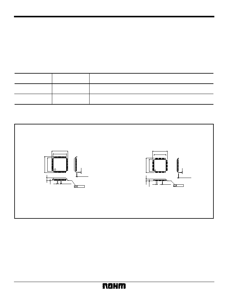
External dimensions (Units: mm)
VQFP64
QFP-A64
BU1425AK
BU1425AKV
0.15
±
0.1
48
33
32
17
49
64
1
16
14.0
±
0.2
16.4
±
0.3
14.0
±
0.2
0.35
±
0.1
0.05
0.5
16.4
±
0.3
0.8
2.7
±
0.1
0.15
48
33
32
17
16
1
49
64
10.0
±
0.2
12.0
±
0.3
10.0
±
0.2
12.0
±
0.3
0.2
±
0.1
0.1
0.5
0.125
±
0.1
0.5
0.10
1.4
±
0.1