 | ÐлекÑÑоннÑй компоненÑ: RCM2122R | СкаÑаÑÑ:  PDF PDF  ZIP ZIP |
Äîêóìåíòàöèÿ è îïèñàíèÿ www.docs.chipfind.ru
RCM2122R
Liquid Crystal Displays
16 character
× 1 line COG module
RCM2122R
RCM2122R is LCD module which controller / driver LSI built in.
For display of 16 character
× 1 line type reflective TN type LCD module.
!Applications
Printer, Copy machine, Facsimile, Telephone, etc
!Features
(1) Wide viewing angle, high contrast ratio.
(2) The dot construction is 5
× 7 dot plus 1 line.
(3) Can be interfaced with 4bit or 8bit MPU.
(4) Can display 190 different types of JIS character and symbols.
(5) With built-in character generator RAM, any user-design pattern can be displayed.
(6) Display clear, cursor ON / OFF, displayed character blink etc,
various function instruction can be accomplished simply.
(7) Compact light weight type, which can be assembled to a machine easily.
(8) Can drive by a 5V circuit.
(9) Low power consumption.
!
!
!
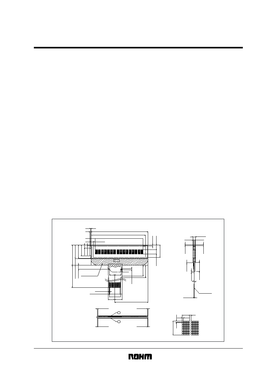
!External dimensions
(Units : mm)
2.62
0.58
0.08
0.46
0.58
0.08
5.2
Dot detail
0.5±0.5
7.5±0.5
1.5Max.
0.5±0.5
0.5±0.5
1.1±0.1
1.1±0.1
2.75±0.3
0.3±0.05
Terminal side
3Max.
(50.62)
57.2Min.
60.2±0.3
4.79±0.3
0.3Max.
1Max.
0.35Min.
3Max.
6.14±0.3
(5.2)
13.7Min.
3.35Min.
13.35Max.
16.35Max.
4.3±0.3
(1.2)
(9)
(11)
(16.7)
7.0±0.3
23.7±0.3
50±1.3
Over-coating regin
1.5
1.2
(6.7) (8.55)
(7.8)
36.6±1.3
15±0.3
(P1.0
×
13)13±0.1
(9.8)
1
14
14
-
0.7±0.1
0.5±0.5
0.5±0.5
0.5±0.5
0.5±0.5
1
2
RCM2122R
Liquid Crystal Displays
!
!
!
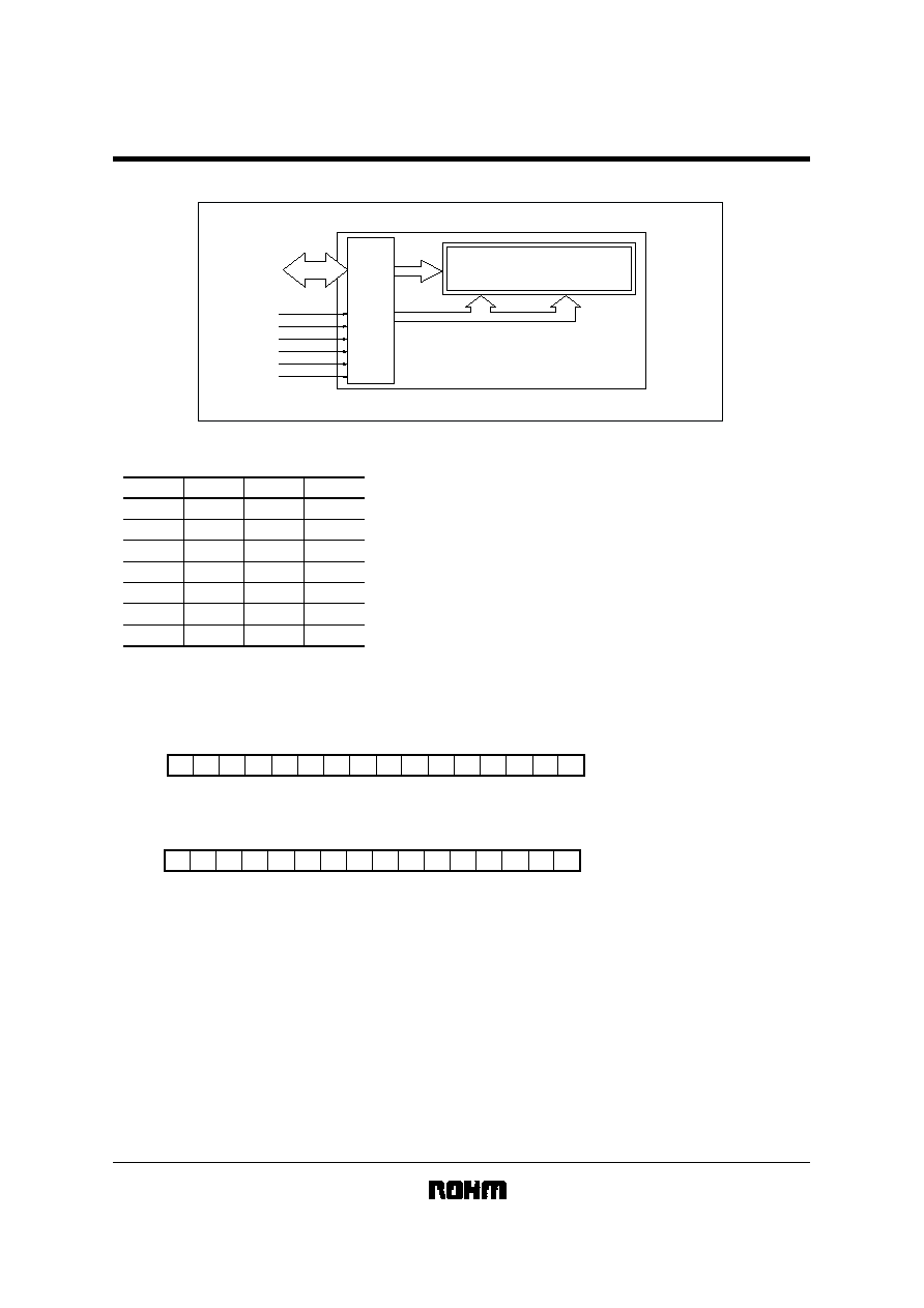
!Block diagram
E
R / W
RS
V
O
V
DD
V
SS
40
40
16
LCD
DB0
DB7
8
IC1
!
!
!
!Pin functions
Pin No.
1
2
3
4
5
6
7
Symbol
Pin No.
Symbol
DB7
8
DB0
DB6
9
E
DB5
10
R / W
DB4
11
R
S
DB3
12
V
O
DB2
13
V
DD
DB1
14
V
SS
!
!
!
!DD RAM Address
(1) Addressing mode 1 (A=0)
00
1 Line
01
02
03
04
05
06
07
08
09
0A
0B 0C
0D
0E
DD RAM ADDRESS
(16H)
0F
1
2
3
4
5
6
7
8
9
10
11
12
13
14
15
16 (Display position)
(2) Addressing mode 2 (A=1)
00
1Line
01
02
03
04
05
06
07
40
41
42
43
44
45
46
DD RAM ADDRESS
(16H)
47
1
2
3
4
5
6
7
8
9
10
11
12
13
14
15
16 (Display position)
Note) The above shows the addresses when the display off is not conducted.
RCM2122R
Liquid Crystal Displays
!
!
!
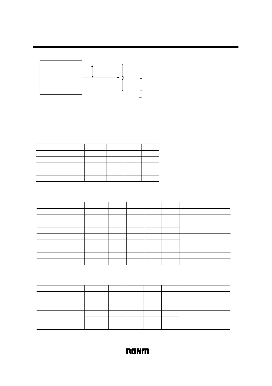
!Power supply sample connect
V
DD
V
DD
-
V
O
V
DD
V
R
: 10k
V
O
LCD MODULE
As operating voltage, (V
DD
-V
O
)V is charged to LCD.
Optimum operating voltage changes by viewing angle and temperature.
Contrast can be changed by adjustment of V
O
, so please use LCD module
at most suitable condition by each operating situation.
When you fix the V
O
, please check using by actual set.
(Note)
V
SS
Fig.1
!
!
!
!Absolute maximum ratings
(Ta=25
°C)
Min.
-
0.3
-
0.3
-
0.3
0
-
20
Symbol
V
DD
-V
SS
V
DD
-V
O
V
IN
Topr
Tstg
Max.
6.0
6.0
V
DD
+
0.3
50
70
Unit
V
V
V
°C
°C
Supply voltage for logics
Supply voltage for driving LCD
Input voltage
Operating temperature rang
Storage temperature rang
Parameter
!
!
!
!Electrical characteristics
(V
DD
=5.0
±5%, Ta=25°C)
Parameter
Supply voltage for logics
Operating voltage
Input "H" level voltage (1)
Input "L" level voltage (1)
Input "H" level voltage (2)
Input "L" level voltage (2)
Output "H" level voltage
Output "L" level voltage
Power supply current
Symbol
V
DD
V
DD
-
V
O
V
IH1
V
IL1
V
IH2
V
IL2
V
OH
V
OL
I
DD
Min.
4.75
3.0
2.3
0
0.8V
DD
0
2.4
-
-
Typ.
5.0
-
-
-
-
-
-
-
1.4
Max.
5.25
V
DD
V
DD
0.8
V
DD
0.2V
DD
-
0.4
3.6
Unit
V
V
V
V
V
V
V
V
mA
Conditions
IOH=
-
0.205mA
IOL=1.6mA
V
DD
=5.0V, fosc=270kHz
All terminals except E terminal
E
!
!
!
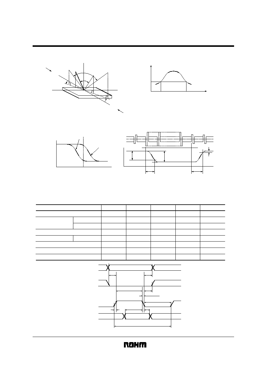
!Optical characteristics
(Ta=25
°C)
Parameter
Rise time
Decay time
Contrast ratio
Viewing angle
Symbol
t
r
t
d
K
1
2
Min.
-
-
1.4
-
40
±30
Typ.
100
150
2.0
-
-
-
Max.
200
250
-
10
-
-
Unit
ms
ms
-
deg
deg
deg
Conditions
=10°,
=0°
=0°, K
1.4
=20°, K
1.4
=10°,
=0°
=10°,
=0°
RCM2122R
Liquid Crystal Displays
Selected
condition
Rise time
Decay time
90%
100%
10%
t
r
t
d
Non-selected
Selected
Brightness (%)
Driving voltage
100
0
B
1
B
2
K=B
2
/ B
1
Viewing angle
Contrast ratio
1.4
1
2
Viewing direction (12:00)
Viewing direction (6:00)
X
X'
2
2'
1
1'
Y [
=180
°
]
Y' [
=0° ]
Z [
=
0° ]
(1) Difinition of
and
(3) Difinition of contrast ratio K
(2) Difinition of viewing angle
1 and
2
(4) Difinition of optical response time
Fig.2
Fig.4
Fig.3
Fig.5
!
!
!
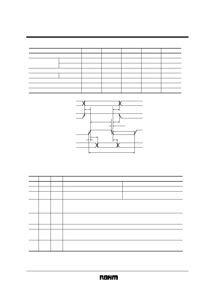
!Timing characteristics
(1) Writing (V
DD
=5V
±5%, V
SS
=0V, Ta=0
+50°C)
Parameter
Enable cycle time
Enable pulse time
Set-up time
Address hold time
Data set-up time
Data hold time
Enable rise time / decay time
"H" level
"L" level
RS, R / W, E
Symbol
t
CYCE
PW
EH
PW
EL
t
Er
,t
Ef
t
AS
t
AH
t
DSW
t
H
Min.
500
220
280
-
40
10
60
10
Max.
-
-
-
20
-
-
-
-
Unit
ns
ns
ns
ns
ns
ns
ns
ns
Fig.6
Fig.6
Fig.6
Fig.6
Fig.6
Fig.6
Fig.6
Fig.6
V
IL1
V
IL1
V
IL2
V
IL2
V
IL2
V
IL1
V
IL1
V
IH1
V
IH1
V
IH2
V
IH1
V
IL1
V
IH1
V
IL1
t
DSW
t
H
V
IH2
t
AS
t
Er
t
AH
t
AH
t
Ef
PW
EH
PW
EL
RS
R / W
E
DB0
DB7
t
CYCE
Valid data
Fig.6
RCM2122R
Liquid Crystal Displays
(2) Reading (V
DD
=5V
±5%, V
SS
=0V, Ta=0
+50°C)
Parameter
Enable cycle time
Enable pulse time
Set-up time
Address hold time
Data set-up time
Data hold time
Enable rise time / decay time
"H" leve
"L" level
RS, R / W, E
Symbol
t
CYCE
PW
EH
PW
EL
t
Er
,t
Ef
t
AS
t
AH
t
DDR
t
DHR
Min.
500
220
280
-
40
10
-
20
Max.
-
-
-
20
-
-
240
-
Unit
ns
ns
ns
ns
ns
ns
ns
ns
Fig.7
Fig.7
Fig.7
Fig.7
Fig.7
Fig.7
Fig.7
Fig.7
Fig.7
V
IL1
V
IL1
V
IL2
V
IL2
V
IL2
V
IH1
V
IH1
V
IH1
V
IH1
V
IH2
V
OH1
V
OL1
V
OH1
V
OL1
t
DDR
t
DHR
V
IH2
t
AS
t
Er
t
AH
t
AH
t
Ef
PW
EH
PW
EL
RS
R / W
E
DB0
DB7
t
CYCE
Valid data
!
!
!
!Pin function
DB4
DB7
DB0
DB3
Symbol
Level
V
SS
V
DD
-
-
-
I / O
-
0V
5.0V
Ground electrical potential
Power voltage
-
-
V
O
R
S
H / L
I
H / L
I
R / W
E
H, H / L
I
Signal to start read or write data
I / O
H / L
H / L
I / O
Function
3.0
5.0V
(V
DD
V
O
)
LCD drive voltage set termination
V
DD
V
O
V
SS
Resistor select signal
0 : Instruction resistor (Write)
Busy flag address counter (Read)
1 : Data resistor (Read / Write)
0 : Write MPU
LCD module
1 : Read MPU
LCD module
Read (R) Write (W) Select signal
Upper level 4 line data bus
Also DB7 is enable to use as busy flag
Lower level 4 line data bus
These pins are not used during 4-bits operation