
SA2030
sames
1/12
n
Delay compensation between switching
stages.
n
Interfacing of PCM systems operating
with different clocks.
n
PCM concentrators and subscriber
multiplexers.
sames
SA2030
PCM FRAME ALIGNER
M74-1885
20.01.93
n
Indication of Slip, loss of frame
synchronisation, and loss of route clock
conditions.
n
ISO-CMOS technology, TTL
Compatible.
n
Pin-for-Pin replacement for Siemens
PEB 2030 and SM 300
n
Microprocessor Interface
APPLICATIONS
n
Delay compensation and clock
alignment between 2,048MHz PCM-
30 transmission lines, and terminating
equipment.
n
Control of Jitter and Wander within
Digital Networks.
GENERAL DESCRIPTION
The SA2030 is designed to interface PCM-30 routes with switching systems. The device
synchronises with the frame-format of the incoming data, and outputs this data in
accordance with the bit and frame timing of the terminating equipment. The circuit is
designed to tolerate delay, drift, wander and jitter of the incoming data and clock, and thus
simplifies the design of data- and clock-recovery hardware. The internal 1� frames
elastic buffer provides for delay compensation and wander immunity. If the bounds of
the buffer are exceeded, the SA2030 will either repeat or drop a frame. The circuit will
accurately detect incoming Alarm-Indication-Signal (AIS) conditions, in accordance with
CCITT recommendation G.737. Loss of frame alignment is indicated on both dedicated
outputs and by outputting of AIS. The circuit includes a bidirectional alarm port for
interrogation of alarm conditions.
FEATURES
n
Frame Alignment Recovery and loss
in accordance with CCITT
recommendations G.732 and G.737
n
Jitter and phase-wander immunity
exceed the requirements of CCITT
recommendation G.823.
n
Internal 1� frame elastic buffer.
n
Detection of incoming Alarm-
Indication-Signal (AIS), and Distant
Alarm
SA2030
sames
2/12
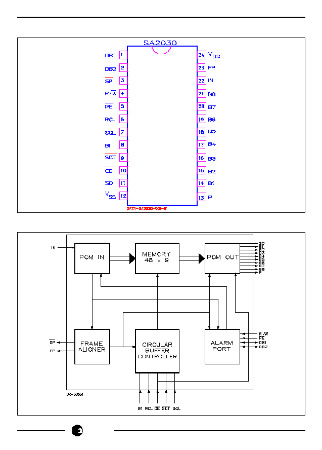
PIN CONFIGURATION
BLOCK DIAGRAM

SA2030
sames
3/12
FUNCTIONAL DESCRIPTION
PCM INPUT AND FRAME-ALIGNMENT
The SA2030 accepts route data on the IN input pin, on rising edges of the route clock RCL.
The circuit synchronises with the frame format of the incoming data by identification of
the Frame Alignment Signal (FAS) and the Service Word (SW) in time slot zero of the
PCM frame. The algorithm used for recovery and loss of frame synchronisation is in
accordance with CCITT recommendation G.737. After the circuit has gained
synchronisation with the incoming PCM-30 data stream, it outputs a synchronisation
pulse SP on alternate frames, during the bit interval prior to time-slot-zero of frames
containing the FAS word. The circuit will output a fault pulse on the FP output every time
errors are detected in the incoming FAS word. When the circuit is unable to synchronise
with the incoming data format, the SA2030 will generate a fault pulse every alternate
frame, and outgoing synchronisation pulses will be suppressed.
PCM OUTPUT
Data is clocked out on falling edges of the System Clock (SCL). PCM output is clocked
out serially on the SO output, and is made available in parallel on a tristate bus with parity
(B1-B8, P). The tristate outputs are enabled by asserting CE. The SA2030 must be
provided with a System Clock Trigger (SCT) pulse to define the required output frame
timing. The SCT pulse defines the bit interval immediately prior to the start of time-slot-
zero, on every alternate frame. Acceptance of SCT pulses is only enabled when CE is
asserted. The tristate parallel bus, with CE control, simplifies the use of the circuit in
multiplex and switching applications.
ELASTIC BUFFER
Incoming PCM data is saved in dual-ported RAM. The RAM has capacity for 1� frames
of data. The SA2030 can thus accommodate any required frame delay between the
incoming data timing, and the required output frame timing. When the bounds of the
buffer are exceeded, whole frames are either dropped or repeated. The action of
dropping or repeating a received frame is called slip. Depending on the frame-delay, the
SA2030 can tolerate between � and 1� frame of wander without requiring to alternately
repeat and drop frames. The design of the elastic buffer controller provides for correct
performance under severe clock-and-data-jitter conditions. The SA2030 exceeds the
requirements of CCITT recommendation G.823, and can be used to control jitter and
wander within digital networks. The 1� frame buffer is enabled by setting BI = 0. If BI
= 1, the buffer length is limited to only one frame. The frame delay through the frame-
aligner is then constrained to be less than one frame. The buffer inhibit mode is useful
for delay compensation within a switching system, where drift and wander do not occur.

SA2030
sames
4/12
ALARM SUBSYSTEM
The alarm system may be used by the host equipment to determine the operation status
of the SA2030. The SA2030 provides a bidirectional alarm-port interface DB1 and DB2.
The direction of the interface is controlled by the R/W line. Transfers to or from the
interface are enabled by strobing the port-enable (PE) input. The circuit includes two 2-
bit alarm registers. The four flags in these registers are set when:
-
Incoming Alarm-Indication-Signal is received (AIS)
-
Loss of frame synchronisation occurs (SYLOSS)
-
A distant alarm is received (DISAL)
-
A frame slip occurs (SLIP)
*
The algorithm used for detection of incoming AIS is in accordance with CCITT
recommendation G.737. That is, AIS will be correctly detected, even in the presence
of random errors, at a rate of 1 in 10
3
.
*
The loss of frame synchronisation flag is set if loss of frame-alignment occurs, if the
route clock is missing or too slow, or if a system-clock-trigger (SCT) pulse is not
applied to the circuit once every alternate frame.
*
The distant alarm flag is set if bit 3 of time-slot-zero of frames not containing FAS
is true.
*
The frame-slip is set if the frame aligner either drops or repeats a frame.
Selection of which of the two alarm registers is to be read, is carried out by first writing
a command to the comand register via DB1 and DB2. Four commands are supported:
-
Enable Read of Alarm Group 1
-
Enable Read of Alarm Group 2
-
Clear all alarm flags
-
Simulate Alarms
Alarm Group 1 includes the AIS and frame synchronisation flags. Alarm Group 2 includes
the Slip and distant alarm flags.
Once an alarm flag is set, it can only be cleared by writing the "clear-all-alarms" command
to the alarm command register. That is, these flags remain set until explicitly cleared.
The simulate-alarm command provides an alarm system self-test capability. This
command simulates all alarm conditions at their sources. If the circuit is operating
correctly, all alarm flags should be set after issuing this command. Alarm simulation tests
the loss of synchronisation function of the frame alignment state-machine, and the AIS
detection logic, and thus may require up to four-frames to complete. After all of the alarm
flags are set, alarm simulation is disabled, and the circuit reverts to normal operation.
SA2030
sames
5/12
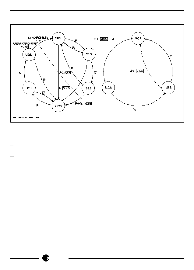
LOSS AND RECOVERY OF FRAME ALIGNMENT
CONDITIONS
R
-
Good FAS Received
R
-
One or more errors in FAS
M
-
Bit 2 of service word = 1 (Good SW)
M
-
Bit 2 of service word = 0 (Bad SW)
UXS
-
Unsynchronised stated U0S, U1S or U2S
M2S
-
Two service word errors received state
STATES
U0S
-
Unsynchronised, zero frames OK state
U1S
-
Unsynchronised, one frame OK state
U2S
-
Unsynchronised, two frame OK state
S0S
-
Synchronised, zero FAS errors state
S1S
-
Synchronised, one FAS error state
S2S
-
Synchronised, two FAS errors state
M0S
-
Zero service word errors state
M1S
-
One service word error state
M2S
-
Two service word errors state