 | –≠–ª–µ–∫—Ç—Ä–æ–Ω–Ω—ã–π –∫–æ–º–ø–æ–Ω–µ–Ω—Ç: adc1342x | –°–∫–∞—á–∞—Ç—å:  PDF PDF  ZIP ZIP |

ADC1342X
0.13
µ
µ
m 10-BIT 30MSPS ADC
1
GENERAL DESCRIPTION
The adc1342x is a CMOS 10-bit low-voltage and high-speed A/D converter (ADC) for video and other
applications. It has a four-step pipelined architecture, which consists of sample & hold amplifier, multiplying D/A
converters (DACs), and subranging flash ADCs.
The maximum conversion rate of adc1342x is 30MSPS and supply voltage is 2.5V single.
FEATURES
--
Resolution
10-bit
-- Differential
linearity
error:
±
1.0LSB
-- Integral
linearity
error:
±
2.0LSB
-- Maximum
conversion
rate:
30MSPS
-- Sample
&
hold
function
implemented
-- Low
power
consumption:
75mW (Typ)
-- Power
supply:
2.5V
single
-- Operation
temperature
range:
≠
40
∞
C ~ 85
∞
C
TYPICAL APPLICATIONS
-- CCD imaging processors
-- Camcorders, scanners, and security cameras.
-- Read channel LSI
HDD, DVD, and CD-ROM drives
-- IF and baseband signal digitizers
-- Portable equipments for low-power applications
0.13
µ
µ
m 10-BIT 30MSPS ADC
ADC1342X
2
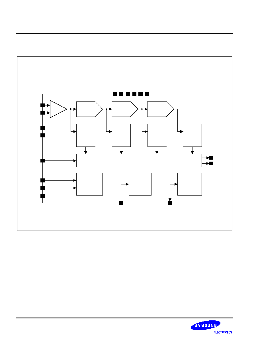
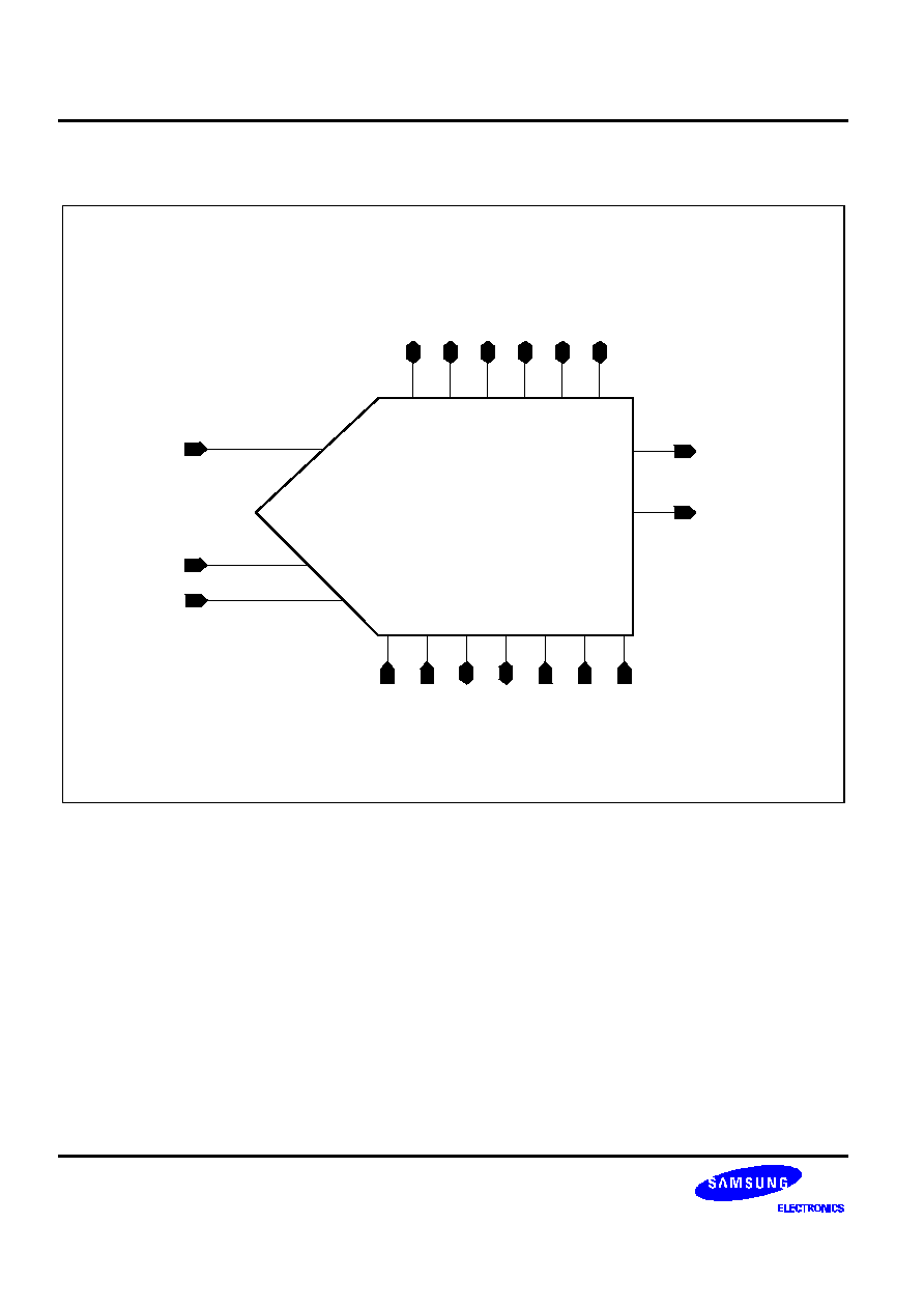
FUNCTIONAL BLOCK DIAGRAM
Flash1
SHA
MDAC1
Flash2
MDAC2
Flash3
MDAC3
Flash4
Digital Correction Logic (DCL)
Bias
Current
Generator
Clock
Generator
CML Level
Generator
STC
PD
ITEST
CKIN
AINT
AINC
EOC
DO[9:0]
CML
REFTOP
REFBOT
AVDD25A
AVSS25A
AVBB25A
AVDD25D
AVSS25D
AVBB25D
SPEEDUP
Ver 1.0 (Apr. 2002)
This data sheet is a preliminary version. No responsibility is assumed by SEC for its use nor for any infringements of patents
or other rights of third parties that may result from its use. The content of this data sheet is subject to change without any
notice.
ADC1342X
0.13
µ
µ
m 10-BIT 30MSPS ADC
3
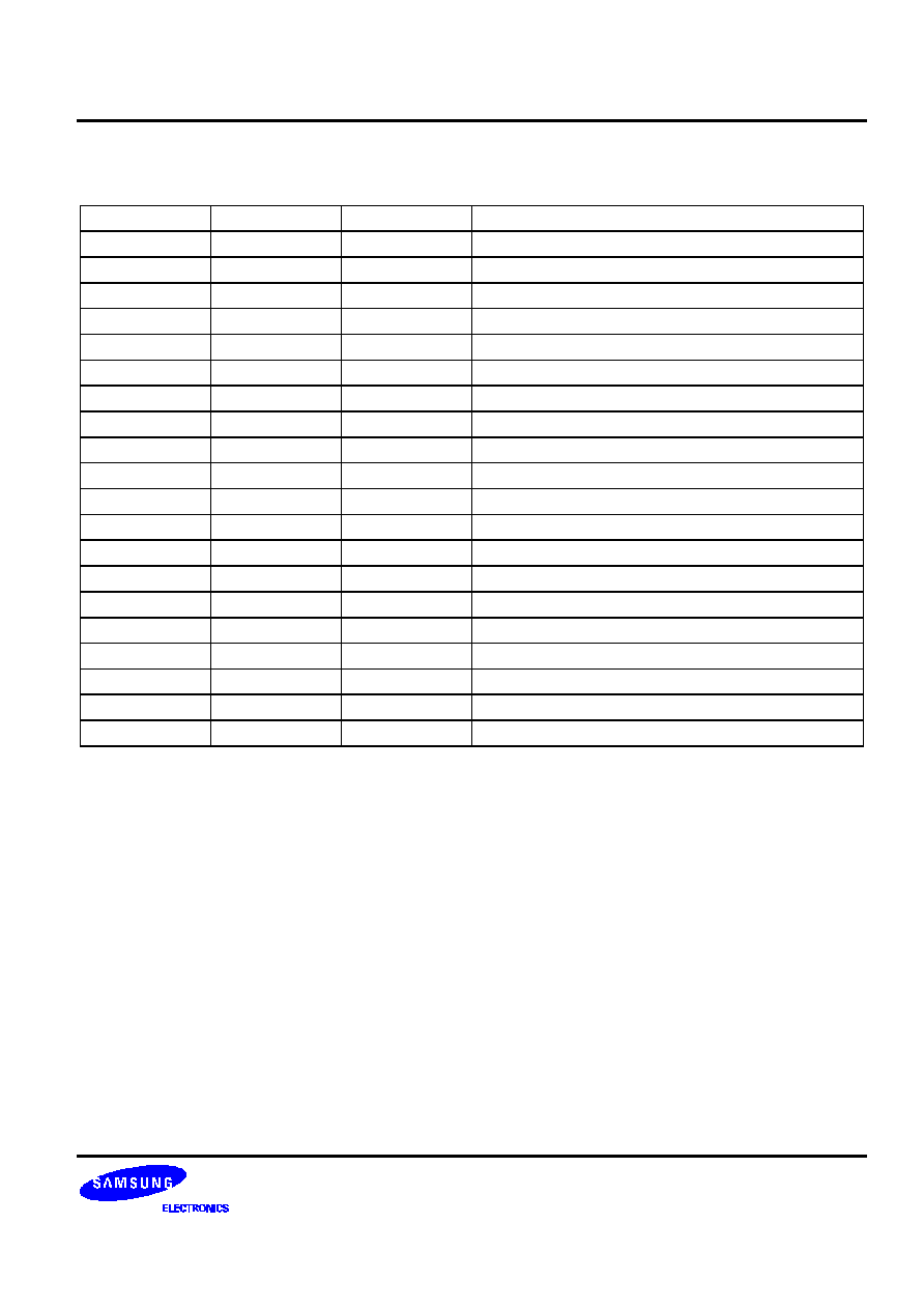
CORE PIN DESCRIPTION
Name
I/O Type
I/O Pad
Pin Description
AINT
AI
pmiar10_abb
Analog
input
+
(
0.95V
~
1.55V)
AINC
AI
pmiar10_abb
Analog
input
-
(1.55V ~ 0.95V)
REFTOP
AI
pmia_abb
Reference
top
(1.55V)
REFBOT
AI
pmia_abb
Reference
bottom (0.95V)
AVDD25A
AP
vdd25tm_abb
Analog
power
(2.5V)
AVSS25A
AG
vsstm_abb
Analog
ground
AVBB25A
AG
vbbm_abb
Analog
sub
bias
ITEST
AB
pmia_abb
Test pin (normally, open)
PD
DI
pmicc_abb
Power down
mode (normally,
gnd)
STC
DI
pmicc_abb
Start
of
conversion
signal
(normally,
high)
SPEEDUP
DI
pmicc_abb
Speed
test
pin (normally,
gnd)
CKIN
DI
pmicc_abb
Sampling
clock
input
CML
AB
pmoa_abb
Test
pin (normally, open)
DO[9:0]
DO
pmot8_abb
Digital
output
EOC
DO
pmot8_abb
End
of
conversion
signal
AVBB25D
DG
vbbm_abb
Digital
sub
bias
AVSS25D
DG
vsstm_abb
Digital
ground
AVDD25D
DP
vdd25tm_abb
Digital
power
I/O
Type
Abbr.
-- AI: Analog Input
-- DI: Digital Input
-- AO: Analog Output
-- DO: Analog Output
-- AP: Analog Power
-- AG: Analog Ground
-- DP: Digital Power
-- DG: Digital Ground
-- AB: Analog Bi-Direction
-- DB: Digital Bi-Direction
0.13
µ
µ
m 10-BIT 30MSPS ADC
ADC1342X
4
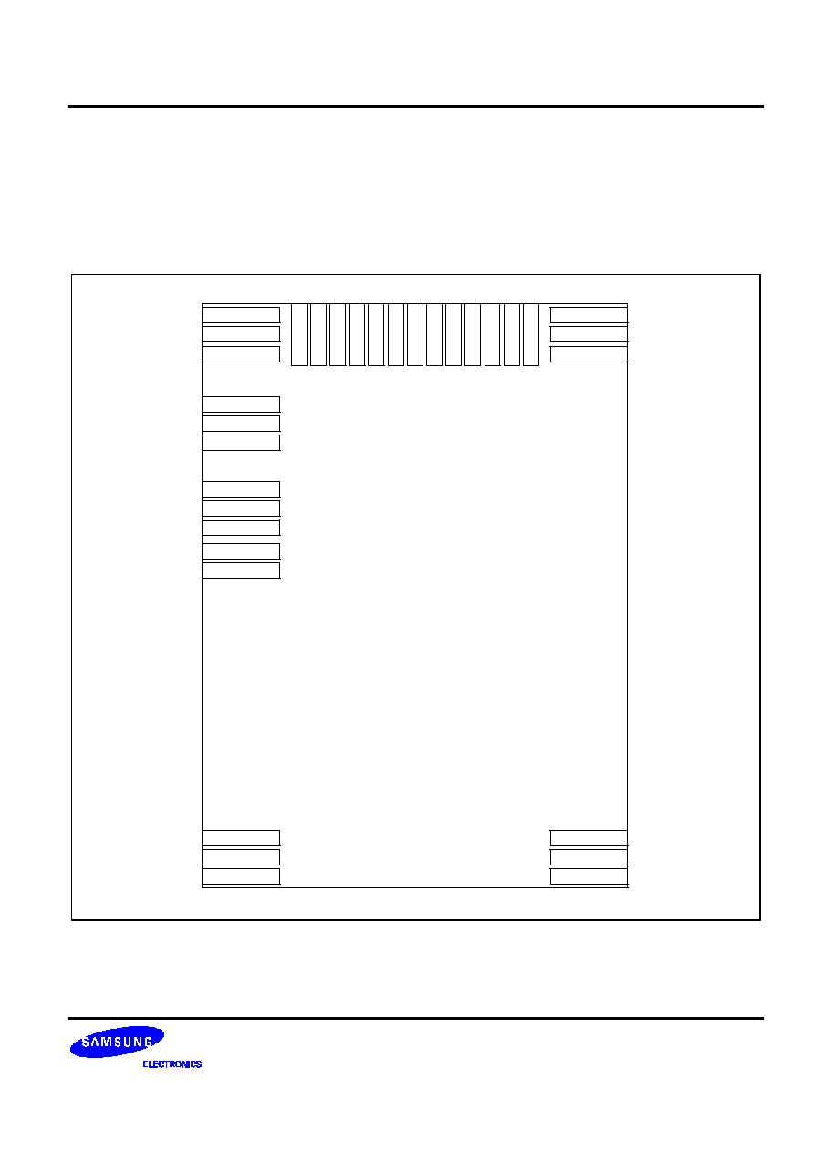
CORE CONFIGURATION
REFTOP
REFBOT
AINT
AINC
CKIN
AVDD25A
AVSS25A
AVBB25A
AVSS25D
AVBB25D
SPEEDUP
DO[9:0]
EOC
STC
PD
CML
ITEST
AVDD25D
adc1342x

ADC1342X
0.13
µ
µ
m 10-BIT 30MSPS ADC
5
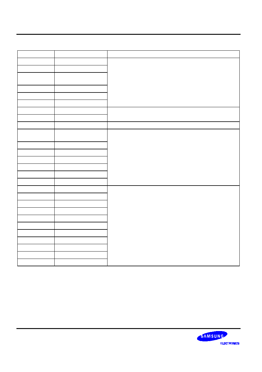
ABSOLUTE MAXIMUM RATINGS
Characteristic
Symbol
Value
Unit
Supply voltage
VDD
3.6
V
Analog input voltage
AIN
VSS to VDD
V
Digital input voltage
CLK
VSS to VDD
V
Digital output voltage
V
OH
, V
OL
VSS to VDD
V
Storage temperature range
Tstg
≠45 to 150
∞
C
NOTES:
1.
Absolute
maximum
rating
specifies
the
values
beyond
which
the
device
may
be
damaged
permanently.
Exposure
to
absolute
maximum
rating
conditions
for
extended
periods
may
affect
reliability.
Each
condition
value
is
applied
with
the
other
values
kept
within
the
following
operating
conditions
and
function
operation
under
any
of
these
conditions
is
not
implied.
2.
All
voltages
are
measured
with
respect
to
VSS
unless
otherwise
specified.
3.
100pF
capacitor
is
discharged
through
a
1.5k
resistor
(Human
body
model).
RECOMMENDED OPERATING
CONDITIONS
Characteristics
Symbol
Min
Typ
Max
Unit
Supply voltage
AVDD25A ≠ AVSS25A
AVDD25D ≠ AVSS25D
2.38
2.5
2.63
V
Supply voltage difference
AVDD25A ≠ AVDD25D
≠0.1
0.0
0.1
V
Reference input voltage (externally)
REFTOP
REFBOT
≠
≠
1.55
0.95
≠
≠
V
Analog input voltage (+)
AINT
0.95
≠
1.55
V
Analog input voltage (-)
AINC
1.55
≠
0.95
V
Operating temperature
Topr
≠40
≠
85
∞
C
NOTE: is
strongly
recommended
that
all
the
supply
pins
(AVDD25A,
AVDD25D)
be
powered
from
the
same
source
to
avoid
power
latch-up.

0.13
µ
µ
m 10-BIT 30MSPS ADC
ADC1342X
6
DC ELECTRICAL
CHARACTERISTICS
Characteristics
Symbol
Min
Typ
Max
Unit
Conditions
Resolution
≠
≠
10
≠
Bits
Reference current
IREF
≠
2
3
mA
Differential linearity error
DLE
≠
≠
±
1.0
LSB
Integral linearity error
ILE
≠
≠
±
2.0
LSB
Bottom offset voltage error
EOB
≠
≠
20
LSB
Top offset voltage error
EOT
≠
≠
20
LSB
NOTES:
1.
Converter
specifications
(unless
otherwise
specified)
AVDD25A=2.5V
AVDD25D=2.5V
AVSS25A=GND
AVSS25D=GND
Ta=25
∞
C
2.
TBD:
To
be
determined
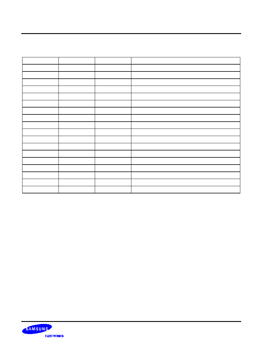
AC ELECTRICAL CHARACTERISTICS
Characteristics
Symbol
Min
Typ
Max
Unit
Conditions
Maximum conversion rate
fc
≠
≠
30
MSPS
≠
Dynamic supply current
Ivdd
≠
30
≠
mA
fc = 30MHz
(without system load)
Digital output data delay
Td
≠
1.8
≠
ns
See
"Timing Diagram"
Signal - to - noise ratio
SNR
48
52
≠
dB
AINT = 1MHz
fc = 30MHz
ADC1342X
0.13
µ
µ
m 10-BIT 30MSPS ADC
7
I/O
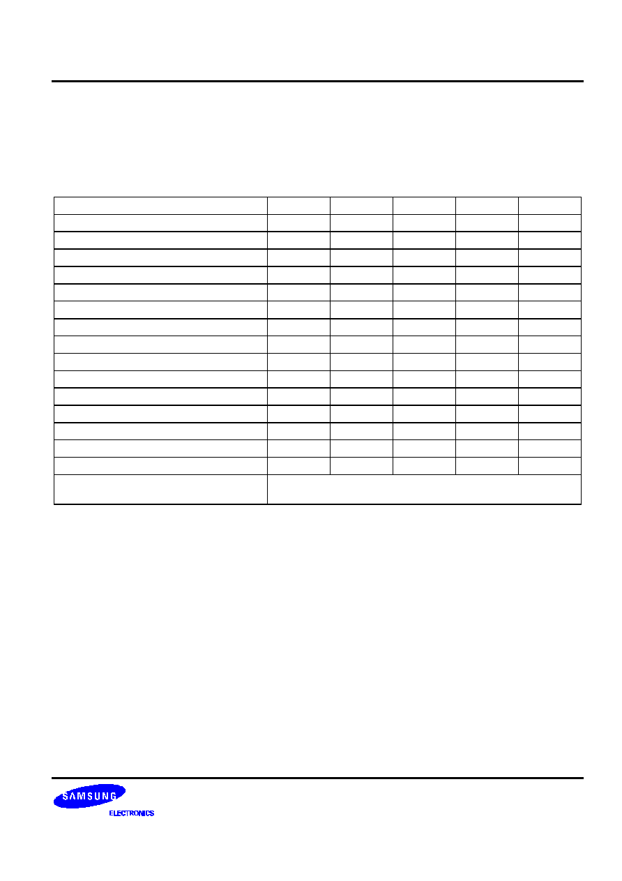
CHART
Index
AINT Input (V)
AINC Input (V)
Digital Output
0
0.950000 ~ 0.950587
1.549413 ~ 1.550000
0000000000
1LSB = 1.1730mV
for differential input
1
0.950587 ~ 0.951174
1.548826 ~ 1.549413
0000000001
REFTOP = 1.55V
2
0.951174 ~ 0.951761
1.548239 ~ 1.548826
0000000010
REFBOT = 0.95V
∑
∑
∑
∑
∑
∑
∑
∑
∑
∑
∑
∑
511
1.249413 ~ 1.250000
1.250578 ~ 1.251174
0111111111
512
1.250000 ~ 1.250578
1.250000 ~ 1.250578
1000000000
513
1.250578 ~ 1.251174
1.249413 ~ 1.250000
1000000001
∑
∑
∑
∑
∑
∑
∑
∑
∑
∑
∑
∑
1021
1.548239 ~ 1.548826
0.951174 ~ 0.951761
1111111101
1022
1.548826 ~ 1.549413
0.950587 ~ 0.951174
1111111110
1023
1.549413 ~ 1.550000
0.950000 ~ 0.950587
1111111111

0.13
µ
µ
m 10-BIT 30MSPS ADC
ADC1342X
8
TIMING DIAGRAM
1. Main Waveform
STC
EOC
DO[9:0]
CKIN
Analog
Input
A6
A2
A1
A4
td
D1
D2
D4
D6
Pipeline Delay
Output code of DO[9:0] is generated during STC (Start of Conversion) signal is just "HIGH". Otherwise, it keeps
the current states.
After STC goes "HIGH", the A/D converter requires the pipeline delay of 3 clock period to generate EOC signal
and DO[9:0].
2. STC & CKIN
8ns
CKIN
STC
4ns
T
SAFE
. . .
. . .
8ns
4ns
T
SAFE
The STC signal is rising-edge triggered, and it should be changed during "T
SAFE
" region on CKIN.

ADC1342X
0.13
µ
µ
m 10-BIT 30MSPS ADC
9
CORE EVALUATION GUIDE
ADC function is evaluated by external check on the bi-directional pads connected to input nodes of HOST DSP
back-end circuit.
The reference voltages may be biased internally through resistor divider.
DO[9:0]
EOC
Digital Mux
HOST
DSP
CORE
Bi-Directional PAD
(ADC Function Measuring &
Digital Input Forcing)
Analog Input
Clock Input
AINT
AINC
CKIN
AVDD25A
AVSS25A
AVBB25A
AVSS25D
AVBB25D
AVDD25D
REFTOP
REFBOT
SPEEDUP
STC
PD
CML
ITEST
10-bit Digital Output
2.5V
GND
2.5V
GND
1.55V
GND
0.95V
GND
Reference
Top
Reference
Bottom
GND
STC Input
or 2.5V
GND
NOTES:
: 10uF electronic capacitor unless otherwise specified
: 0.1uF ceramic capacitor unless otherwise specified
adc1342x

0.13
µ
µ
m 10-BIT 30MSPS ADC
ADC1342X
10
PACKAGE CONFIGURATION
adc1342x_top
48
47
REFTOP
REFTOP
REFBOT
REFBOT
CML
AVDD25A
AVDD25A
AVBB25A
AVSS25A
AVSS25A
AINT
NC
AINC
NC
SPEEDUP
ITEST
PD
AVDD25R
AVSS25R
CKIN
NC
NC
NC
NC
AVDD25D
AVDD25D
AVSS25D
AVDD25D
STC
NC
NC
NC
NC
DO[9]
DO[8]
DO[7]
DO[6]
DO[5]
DO[4]
DO[3]
DO[2]
DO[1]
DO[0]
NC
0.1u
10u
EOC
46
45
44
43
42
41
40
39
38
37
36
35
34
33
32
31
30
29
28
27
26
25
1
2
3
4
5
6
7
8
9
10
11
12
13
14
15
16
17
18
19
20
21
22
23
24
0.1u
10u
10u
0.1u
NC
NC
NC
10-bit ADC
Output
STC In
EOC Out
2.5V
1.55V
10u
0.1u
0.95V
0.1u
2.5V
10u
0.1u
0.1u
50
1K
0.1u
Clock In
2.5V
50
Test Pin
No bisa forcing, remain floating
Analog
Input
0.1u
NOTE: This information is for testing the provided test-chips of ADC1342X.
ADC1342X
0.13
µ
µ
m 10-BIT 30MSPS ADC
11
PACKAGE PIN DESCRIPTION
Name
Pin No.
I/O Type
Pin Description
REFTOP
1, 2
AI
External reference top bias (1.55V)
REFBOT
3, 4
AI
External reference bottom bias (0.95V)
CML
5
AB
Internal bias point (test pin)
AVDD25A
6, 7
AP
Analog power (2.5V)
AVBB25A
8
AG
Analog sub bias
AVSS25A
9, 10
AG
Analog ground
AINT
11
AI
Analog input + (Input range: 0.95~1.55V differential)
AINC
13
AI
Analog input. - (Input range: 1.55~0.95V differential)
SPEEDUP
15
DI
Speed test pin. Tie to analog GND
ITEST
16
AB
Open = Use internal bias point
PD
17
DI
Power Down mode (normally gnd)
AVDD25R
18
PP
Output driver power (2.5V)
AVSS25R
19
PG
Output driver ground
CKIN
20
DI
Sampling clock input
DO[9:0]
27~36
DO
10-bit digitized output
EOC
42
DO
End of conversion signal
STC
43
DI
Start of conversion signal
AVBB25D
44
DG
Digital substrate bias
AVSS25D
45, 46
DG
Digital ground
AVDD25D
47, 48
DP
Digital power (2.5V)
NOTES:
1.
This information is for testing the provided test-chips of ADC1342X.
2.
I/O
TYPE
PP
and
PG
denote
PAD
Power
and
PAD
Ground
respectively.

0.13
µ
µ
m 10-BIT 30MSPS ADC
ADC1342X
12
USER GUIDE
1. Input Signal Range
The ADC was designed to use both single and differential mode input, but the differential mode is recommended
to guarantee the operating margin in the low voltage condition.
-- Differential Mode Input Condition
Pin
Input Range
Conditions
AINT
0.95V ~ 1.55V
AINC
1.55V ~ 0.95V
180
∞
phase shifted input with the same DC level with AINT
-- Single Mode Input Condition
Pin
Input Range
Conditions
AINT
0.65V ~ 1.85V
AINC
1.25V
Forced from the clean DC source or CML pin of ADC1342X
2. Input Signal Speed
Normal speed range of ADC1342X is 1MHz ~ 4MHz input quantized by 30MHz clock, which is fixed by a normal
video signal format.
ADC1342X
0.13
µ
µ
m 10-BIT 30MSPS ADC
13
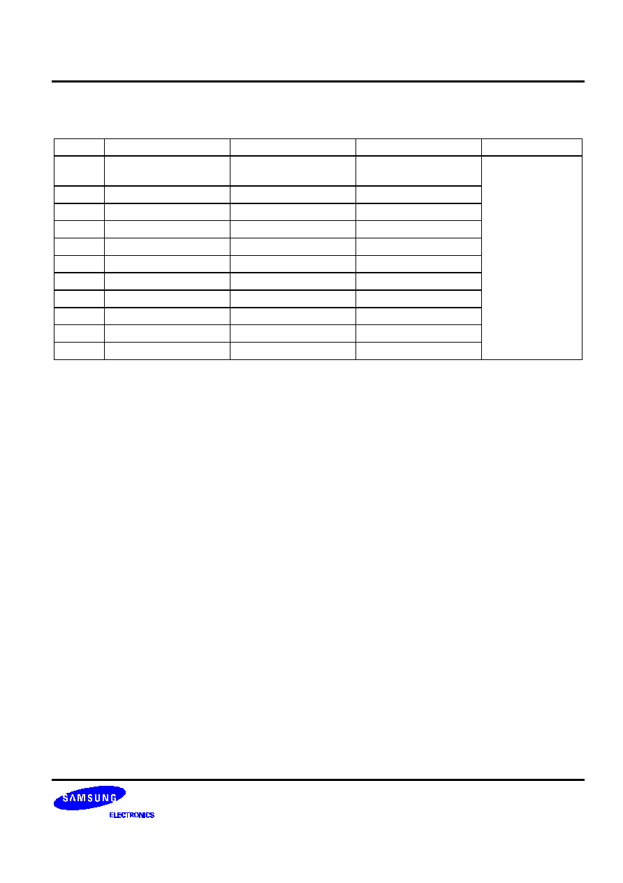
PHANTOM CELL INFORMATION
Pins of the core can be assigned externally (package pins) or internally (internal ports) depending on design
methods.
The term "External" implies that the pins should be assigned externally like power pins.
The term "External/internal" implies that the applications of these pins depend on the user.
adc1342X
10-bit 30MSPS adc
AVDD25D
AVBB25D
AVSS25D
EOC
STC
DO[9]
DO[8]
DO[7]
DO[6]
DO[5]
DO[4]
DO[3]
DO[2]
DO[1]
DO[0]
CKIN
AVDD25D
AVBB25D
AVSS25D
PD
SPEEDUP
ITEST
REFBOT
CML
REFTOP
AINT
AINC
AVSS25A
AVBB25A
AVDD25A
AVSS25A
AVBB25A
AVDD25A
0.13
µ
µ
m 10-BIT 30MSPS ADC
ADC1342X
14
Pin Name
Pin Usage
Pin Layout Guide
AVDD25A
External
Maintain the large width of lines as far as the pads.
AVSS25A
External
Place the port positions to minimize the length of power lines.
AVBB25A
External
Do not merge the analog powers with anoter power from other
blocks.
AVDD25A
External
Use good power and ground source on board.
AVSS25D
External
AVBB25D
External
AINT
External / Internal
Do not overlap with digital lines.
AINC
External / Internal
Maintain the shotest path to pads.
CKIN
External / Internal
Separate from all other analog signals
REFTOP
External / Internal
Maintain the larger width and the shorter length as far as the
pads.
REFBOT
External / Internal
Separate from all other digital lines.
CML
External / Internal
ITEST
External / Internal
PD
External / Internal
STC
External / Internal
SPEEDUP
External / Internal
EOC
External / Internal
Separated from the analog clean signals if possible.
DO[9]
External / Internal
Do not exceed the length by 1,000um.
DO[8]
External / Internal
DO[7]
External / Internal
DO[6]
External / Internal
DO[5]
External / Internal
DO[4]
External / Internal
DO[3]
External / Internal
DO[2]
External / Internal
DO[1]
External / Internal
DO[0]
External / Internal
ADC1342X
0.13
µ
µ
m 10-BIT 30MSPS ADC
15
FEEDBACK
REQUEST
It should be quite helpful to our ADC core development if you specify your system requirements on ADC in the
following characteristic checking table and fill out the additional questions.
We appreciate your interest in our products. Thank you very much.
Characteristic
Min
Typ
Max
Unit
Remarks
Analog power supply voltage
V
Digital power supply voltage
V
Bit resolution
Bit
Reference input voltage
V
Analog input voltage
Vpp
Operating temperature
∞
C
Integral non-linearity error
LSB
Differential non-linearity error
LSB
Bottom offset voltage error
mV
Top offset voltage error
mV
Maximum conversion rate
MSPS
Dynamic supply current
mA
Power dissipation
mW
Signal-to-noise ratio
dB
Pipeline delay
CLK
Digital output format (provide detailed
description & timing diagram)
-- Between single input-output and differential input-output configurations, which one is suitable for your system
and why?
-- Please comment on the internal/external pin configurations you want our ADC to have, if you have any
reason to prefer some type of configuration.
-- Freely list those functions you want to be implemented in our ADC, if you have any.

0.13
µ
µ
m 10-BIT 30MSPS ADC
ADC1342X
16
HISTORY CARD
Version
Date
Modified Items
Comments
Ver1.0
02. 04.01
Original version published (preliminary)
Change the reference range from "0.6V~1.2V" to "0.5V~1.3V"