 | –≠–ª–µ–∫—Ç—Ä–æ–Ω–Ω—ã–π –∫–æ–º–ø–æ–Ω–µ–Ω—Ç: adc1358x | –°–∫–∞—á–∞—Ç—å:  PDF PDF  ZIP ZIP |

SEC ASIC
ADC1358X
3-Ch 10-BIT 3MSPS ADC
Analog core
/11
The ADC1358X is a CMOS 3-Channel 10-bit analog-
to-digital converter (ADC). It converts the analog
input signal into 10bit binary digital codes at a
maximum sampling rate of 3MHz.
The device is a monolithic ADC with on-chip, high-
performance, sample-and-hold Amplifiers (SHA)s and
current reference.
The structure allows single-ended
input.
∑ Resolution : 10-bit
∑ Analog Input Type : R, G, B 3-Channel
∑ Maximum Conversion Rate : 3MHz
∑ Power Supply : 3.3V
∑ Power Consumption : 56mW (typical)
∑ Reference Voltage : 1.65~3.3V, 0.0~0.65V
(variable dual reference)
∑ Input Range : REFTOP ~ REFBOT
∑ Differential Linearity Error : ±1.0 LSB
∑ Integral Linearity Error : ±3.0 LSB
∑ Signal to Noise & Distortion Ratio : 48dB
∑ Digital Output : CMOS Level
∑ Operating Temperature Range : -40∞C
~ 85
∞C
GENERAL DESCRIPTION
FEATURES
High Definition TV (HDTV)
Video Applications & printer
CCD Imaging (Copiers, Scanners, Cameras)
Medical Imaging
Digital Communications
TYPICAL APPLICATIONS
3-Ch 10-BIT 3MSPS ADC
ADC1358X
SAMSUNG ELECTRONICS Co. LTD
Ver 2.0 (MAR. 2002)
This datasheet is a preliminary version. No responsibility is assumed by SEC for its use nor for any
infringements of patents or other rights of third parties that may result from its use. The content of this
data sheet is subject to change without any notice.
FUNCTIONAL BLOCK DIAGRAM
SHA
MDAC
2
MDAC
1
MDAC
3
FLASH
1
FLASH
2
FLASH
3
FLASH
4
DIGITAL
LOGIC
MAIN
BIAS
CLOCK
GEN.
CML
GEN
AINR
REFTOP
REFBOT
CKIN
DO[9:0]
SHA
AING
SHA
AINB
SAMP
RCK
GCK
BCK
PD

SEC ASIC
ADC1358X
3-Ch 10-BIT 3MSPS ADC
Analog core
/11
CORE PIN DESCRIPTION
NAME
I/O TYPE
I/O PAD
PIN DESCRIPTION
REFTOP
AI
phia_abb
Reference Top Force (2.3~3.3V)
REFBOT
AI
phia_abb
Reference Bottom Force (0.0~1.0V)
AVDD33A
AP
vdd3t_abb
Analog Power (3.3V)
AVBB33A
AG
vbb3_abb
Analog Sub Bias
AVSS33A
AG
vss3t_abb
Analog Ground
AINR
AI
phiar50_abb
Analog Input (R Channel)
(Input Range : REFTOP~REFBOT)
AING
AI
phiar50_abb
Analog Input (G Channel)
(Input Range : REFTOP~REFBOT)
AINB
AI
phiar50_abb
Analog Input (B Channel)
(Input Range : REFTOP~REFBOT)
SAMP
DI
picc_abb
R, G, B Input Sampling Clock
RCK
DI
picc_abb
R-Channel Conversion Start Clock
GCK
DI
picc_abb
G-Channel Conversion Start Clock
BCK
DI
picc_abb
B-Channel Conversion Start Clock
PD
DI
picc_abb
Powerdown mode(norminally, gnd)
CKIN
DI
picc_abb
Sampling Clock Input
DO[9:0]
DO
pot2_abb
Digital Output
AVSS33D
DG
vss3t_abb
Digital GND
AVDD33D
DP
vdd3t_abb
Digital Power (3.3V)
AVDD18D
DP
vdd1t_abb
Digital Power (1.8V)
I/O TYPE ABBR.
∑
AI : Analog Input
∑
DI : Digital Input
∑
AO : Analog Output
∑
DO : Analog Output
∑
AP : Analog Power
∑
AG : Analog Ground
∑
DP : Digital Power
∑
DG : Digital Ground
∑
AB : Analog Bidirection
∑
DB : Digital Bidirection
2
adc1358x
PD
CKIN
AINR
REFTOP
REFBOT
DO[9:0]
AING
AINB
SAMP RCK BCK GCK
A
V
D
D
3
3
A
A
V
S
S
3
3
A
A
V
B
B
3
3
A
A
V
D
D
3
3
D
A
V
S
S
3
3
D
A
V
D
D
1
8
D

SEC ASIC
ADC1358X
3-Ch 10-BIT 3MSPS ADC
Analog core
/11
ABSOLUTE MAXIMUM RATINGS
Characteristics
Symbol
Value
Unit
Supply Voltage
VDD33
4.5
V
VDD18
2.4
Analog Input Voltage
AINR, AING, AINB
VSS to VDD33
V
Digital Input Voltage
SAMP, RCK, BCK, GCK,
CKIN, PD
VSS to VDD18
V
Digital Output Voltage
V
OH
, V
OL
VSS to VDD18
V
Storage Temperature Range
Tstg
-45 to 150
∞C
NOTES
1. Absolute maximum rating specifies the values beyond which the device may be damaged permanently. Exposure to
ABSOLUTE MAXIMUM RATING conditions for extended periods may affect reliability. Each condition value is
applied with the other values kept within the following operating conditions and function operation under any of
these conditions is not implied.
2. All voltages are measured with respect to VSS unless otherwise specified.
3. 100pF capacitor is discharged through a 1.5k
resistor (Human body model)
RECOMMENDED OPERATING CONDITIONS
Characteristics
Symbol
Min
Typ
Max
Unit
Supply Voltage
AVDD33D
AVDD33A
3.15
3.3
3.45
V
AVDD18D
1.7
1.8
1.9
V
Internal Reference Input
Voltage
REFTOP
REFBOT
1.65
0.0
1.8
-
3.3
0.65
V
Analog Input Voltage
AINR, AING, AINB
REFBOT
REFTOP
V
Operating Temperature
Toper
-40
-
85
°…
NOTES
It is strongly recommended that all the supply pins (AVDD33A, AVDD33D, AVDD18D) be powered from the
same source to avoid power latch-up.
3

SEC ASIC
ADC1358X
3-Ch 10-BIT 3MSPS ADC
Analog core
/11
DC ELECTRICAL CHARACTERISTICS
Characteristics
Symbol
Min
Typ
Max
Unit
Test Condition
Resolution
RES
-
10
-
bits
Differential
Linearity Error
DNL
-
-
±1.0
LSB
Integral
Linearity Error
INL
-
-
±3.0
LSB
Bottom Offset
Voltage Error
EOB
-
-
25
LSB
Top Offset
Voltage Error
EOT
-
-
25
LSB
NOTES
1. Converter Specifications (unless otherwise specified)
AVDD33A=3.3V
AVDD33D=3.3V AVDD18D=1.8V
AVSS33A=GND
AVSS33D=GND
Ta=25∫C
AC ELECTRICAL CHARACTERISTICS
Characteristics
Symbol
Min
Typ
Max
Unit
Test Condition
Maximum
Conversion Rate
fc
-
-
3
MHz
AIN = AINR or AING
or AINB
Dynamic Supply
Current
IVDD
-
17
20
mA
fc=3MHz
(without system load)
Total Harmonic
Distortion
THD
-
-58
-52
dB
AIN=200KHz
Signal-to-Noise &
Distortion Ratio
SNDR
48
52
-
dB
AIN=200KHz
I/O CHART
4
SEC ASIC
ADC1358X
3-Ch 10-BIT 3MSPS ADC
Analog core
/11
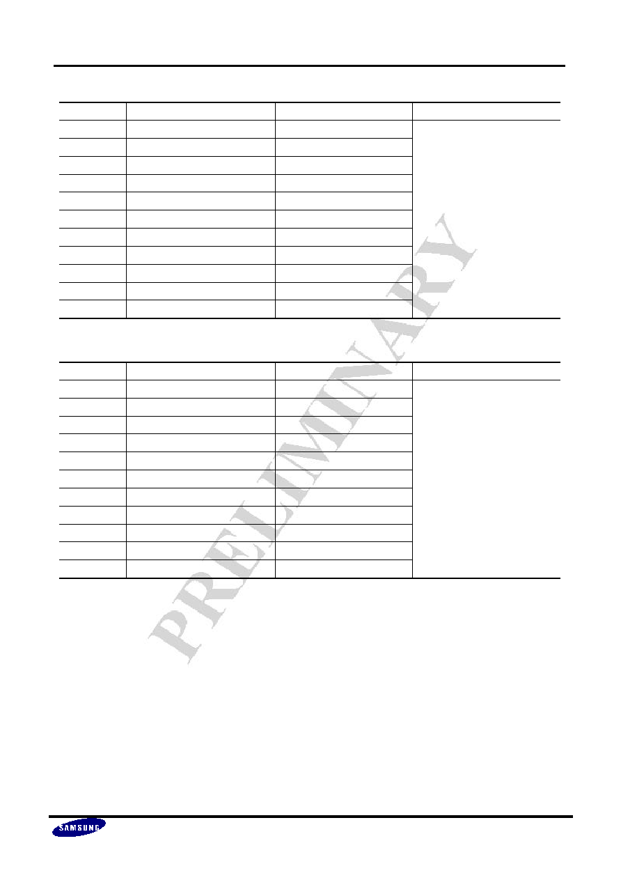
Index
AINR, AING, AINB Input (V)
Digital Output
comment
0
0.00000 ~ 0.00176
0000000000
Input range:0~1.8
1LSB=1.758mV
1
0.00176 ~ 0.00352
0000000001
2
0.00352 ~ 0.00528
0000000010
°
°
°
511
0.89824 ~ 0.90000
0111111111
512
0.90000 ~ 0.90176
1000000000
513
0.90176 ~ 0.90352
1000000001
°
°
°
1021
1.79472 ~ 1.79648
1111111101
1022
1.79648 ~ 1.79824
1111111110
1023
1.79824 ~ 1.80000
1111111111
Index
AINR, AING, AINB Input (V)
Digital Output
comment
0
0.00000 ~ 0.00293
0000000000
Input range:0~3.0
1LSB=2.930mV
1
0.00293 ~ 0.00586
0000000001
2
0.00586 ~ 0.00879
0000000010
°
°
°
511
1.49707 ~ 1.50000
0111111111
512
1.50000 ~ 1.50293
1000000000
513
1.50293 ~ 1.50586
1000000001
°
°
°
1021
2.99121 ~ 2.99414
1111111101
1022
2.99414 ~ 2.99707
1111111110
1023
2.99707 ~ 3.00000
1111111111
5