 | –≠–ª–µ–∫—Ç—Ä–æ–Ω–Ω—ã–π –∫–æ–º–ø–æ–Ω–µ–Ω—Ç: AFE1400X | –°–∫–∞—á–∞—Ç—å:  PDF PDF  ZIP ZIP |

0.35
µ
µ
µ
µ
m 12-BIT 20MSPS AFE FOR CCD/CIS SIGNAL PROCESSOR
AFE1400X
1
GENERAL
DESCRIPTION
The samsung analog front end(AFE) for CCD/CIS image signal is an integrated analog signal processor for color
image signal.
The AFE converts CCD/CIS output signal to digital data. The AFE includes three-channel CDS(Correlated Double
Sampling) circuit, PGA(Programmable Gain Amplifier), and 12-bit analog to digital converter with reference
generator.
The 12-bit digital output is multiplexed into an 8-bit output word that is accessed using 8+4 format two read cycles.
The internal resgisters are programmed through a 3-wire serial interface, and provide adjustment of the gain,
offset, and operating mode.
APPLICATIONS
-- Color and B/W Scanner
-- Digital Copiers
-- General Purpose CCD/CIS imager
FEATURES
-- 12-bit 20 MSPS A/D Converter
-- Integrated Triple Correlated Double Sampler
-- 3-Channel 2 MSPS Color Mode
-- 1 ~ 6.25x Analog Programmable Gain Amplifier
-- Internal Voltage Reference
-- No Missing Code Guaranteed
-- Multiplexed Byte-Wide Output (8+4 Format)
-- 3-Wire Serial Digital Interface
-- Operation by Single 3.3V Supply
-- CMOS Low Power Dissipation
-- 28-SOP-375 Package
KEY
SPECIFICATION
-- Resolution: 12-bit
-- Conversion Rate: 20 MHz(2 MHz*3)
-- Supply Voltage: 3.3 V ± 5%
-- Power Dissipation: 415 mW(Typical)
AFE1400X
0.35
µ
µ
µ
µ
m 12-BIT 20MSPS AFE FOR CCD/CIS SIGNAL PROCESSOR
2
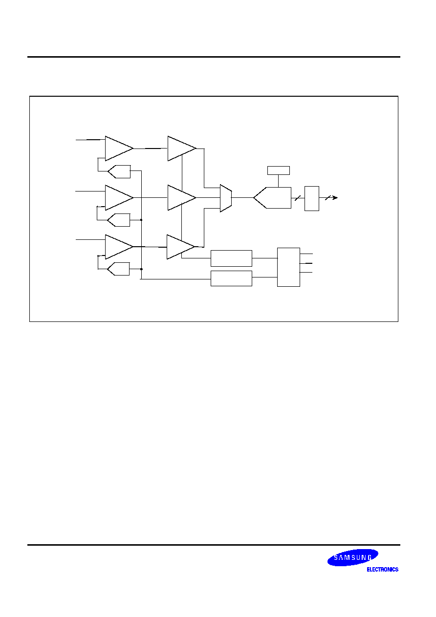
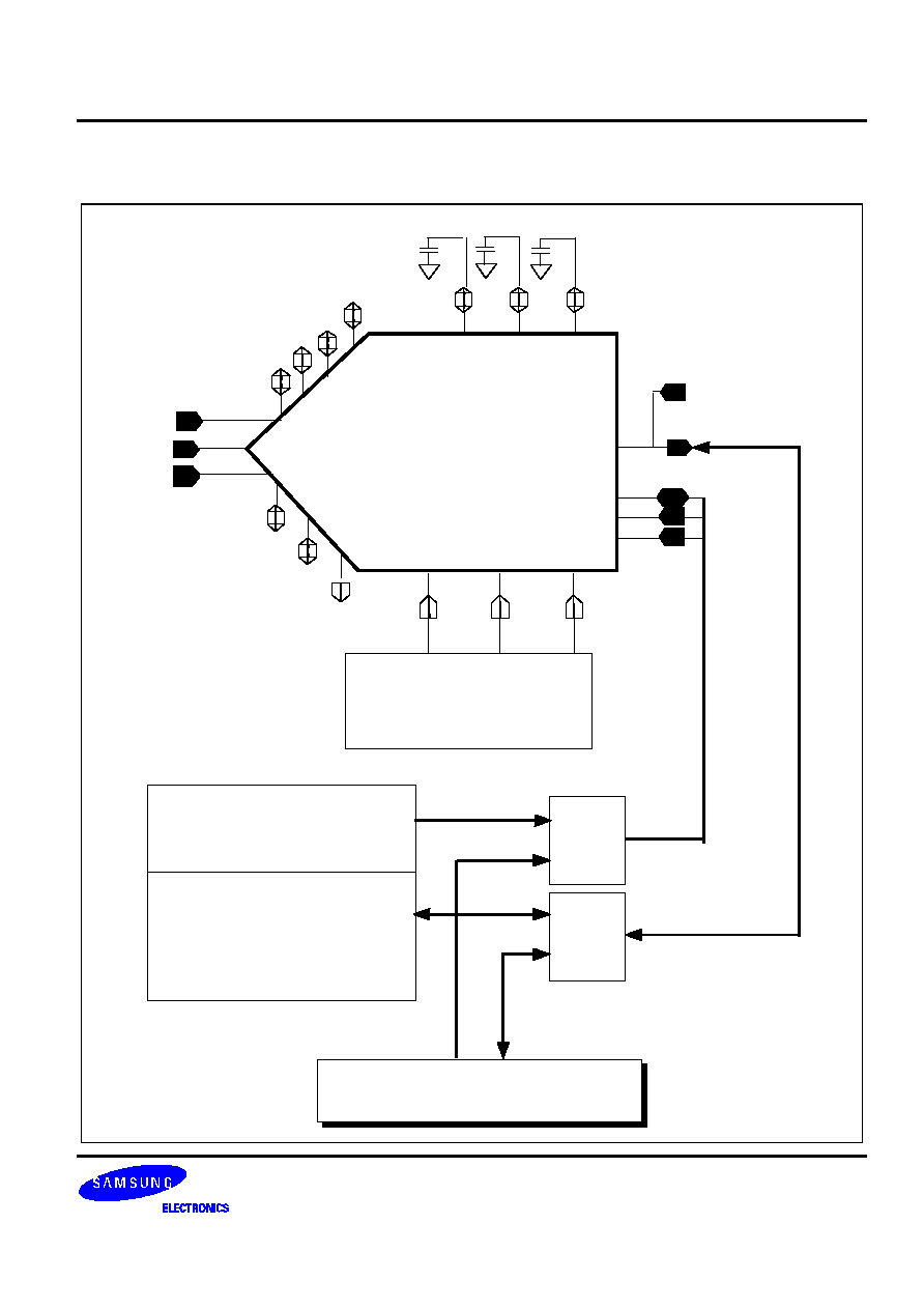
FUNCTIONAL BLOCK DIAGRAM
R ED
C D S
C D S
C D S
PG A
PG A
PG A
MUX
1 2b
AD C
R EF
D [7:0]
I N P U T O F F S E T
R E G I S T E R S
G R EEN
BLU E
G A I N
R E G I S T E R S
D AC
D AC
D AC
M PU
PO R T
8
S CLK
S LO A D
S DATA
O EB
1 2:8
M U X
1 2

0.35
µ
µ
µ
µ
m 12-BIT 20MSPS AFE FOR CCD/CIS SIGNAL PROCESSOR
AFE1400X
3
CORE
PIN
DESCRIPTION
Name
I/O Type
I/O Pad
Description
AVDDA
AP
vdda
3.3 V Analog Supply
AVSSA
AG
vssa
Analog Ground
AVDDD
AP
vdda
3.3 V Digital Supply
AVSSD
AG
vssa
Digital Ground
AVBBA
AG
vbba
Analog Substrate
AVBBD
AG
vbba
Digital Substrate
REFT
AB
poa_bb
Reference Decoupling
REFB
AB
poa_bb
Reference Decoupling
VCOM
AB
poa_bb
Analog Common Voltage
R_VIN
AI
piar10_bb
Analog Input; Red
G_VIN
AI
piar10_bb
Analog Input; Green
B_VIN
AI
piar10_bb
Analog Input; Blue
OFFSET
AB
piar10_bb
Clamp Bias Level Decoupling
CDS1_CLK
DI
picc_bb
CDS Reset Clock Pulse Input
CDS2_CLK
DI
picc_bb
CDS Data Clock Pulse Input
ADCCLK
DI
picc_bb
A/D Converter Sample Clock Input
SDATA
DB
poa_bb
Serial Interface Data Input/Output
SCLK
DI
picc_bb
Serial Interface Clock Input
SLOAD
DI
picc_bb
Serial Interface Load Pulse
OEB
DI
picc_bb
Output Enable; Active Low
D[7:0]
DO
pot4_bb
Data Outputs
I/O Type Abbr.
-- AI: Analog Input
-- DI: Digital Input
-- AO: Analog Output
-- DO: Digital Output
-- AB: Analog Bidirectional
-- DB: Digital Bidirectional
-- AP: Analog Power
-- DP: Digital Power
-- AG: Analog Ground
-- DG: Digital Ground

AFE1400X
0.35
µ
µ
µ
µ
m 12-BIT 20MSPS AFE FOR CCD/CIS SIGNAL PROCESSOR
4
CODE CONFIGURATION
afe_cip4
ADCCLK
D[7:0]
REFT
SDATA
SCLK
SLOAD
CDS2_CLK
CDS1_CLK
G_VIN
B_VIN
R_VIN
VCOM REFB
AVDDA
AVSSA
AVDDD
AVSSD
AVBBA
OEB
OFFSET
AVBBD
ABSOLUTE MAXIMUM
RATINGS
Characteristic
Symbol
Value
Unit
Supply Voltage
VDD
4.5
V
Analog Input Voltage
AIN
VSS to VDD
V
Digital Input Voltage
CLK
VSS to VDD
V
Digital Output Voltage
V
OH
, V
OL
VSS to VDD
V
Reference Voltage
VRT/VRB
VSS to VDD
V
Storage Temperature Range
Tstg
-45 to 150
∞
C
Operating Temperature Range
Topr
0 to 70
∞
C
NOTES:
1.
ABSOLUTE
MAXIMUM
RATING
specifies
the
values
beyond
which
the
device
may
be
damaged
permanently.
Exposure
to
ABSOLUTE
MAXIMUM
RATING
conditions
for
extended
periods
may
affect
reliability.
Each
condition
value
is
applied
with
the
other
values
kept
within
the
following
operating
conditions
and
function
operation
under
any
of
these
conditions
is
not
implied.
2.
All
voltages
are
measured
with
respect
to
VSS
unless
otherwise
specified.
3.
100pF
capacitor
is
discharged
through
a
1.5k
resistor
(Human
body
model)
0.35
µ
µ
µ
µ
m 12-BIT 20MSPS AFE FOR CCD/CIS SIGNAL PROCESSOR
AFE1400X
5
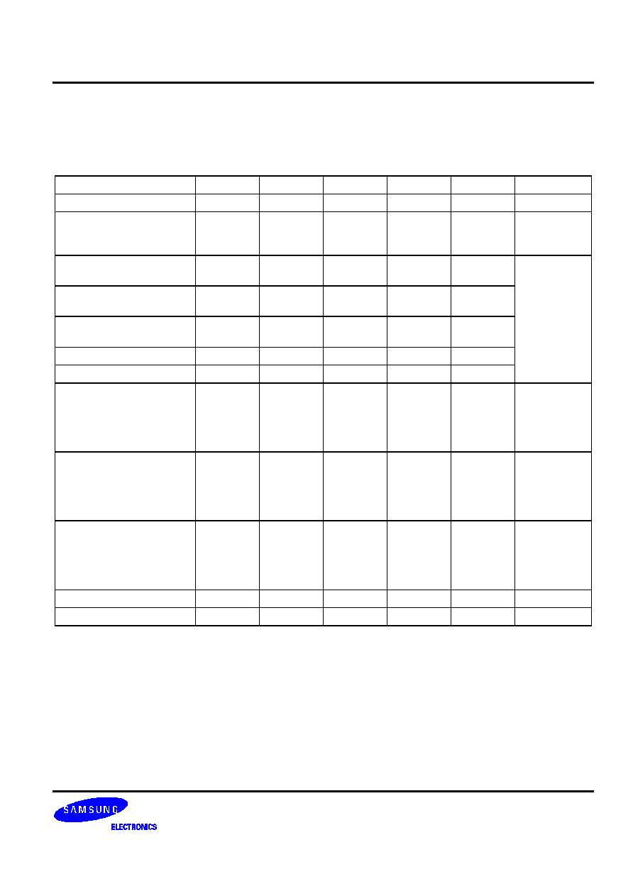
ANALOG SPECIFICATIONS
(VDDA1=3.3V, VDDA2=3.3V, ADCCLK=20MHz, CDS1_CLK=6.666MHz,CDS2_CLK=6.666MHz, PGA Gain=1
unless otherwise noted)
Characteristics
Symbol
Min
Typ
Max
Unit
Comment
Resolution
12
Bits
Conversion Rate
3-Channel with CDS
1-Channel with CDS
20
20
MSPS
MSPS
Signal-to-Noise & Distortion
Ratio @ 1MHz Input
SNDR
60
dB
Entire
Signal Path
Differential
Nonlinearity
DNL
±
1
LSB
Integral
Nonlinearity
INL
±
2
LSB
Unipolar Offset Error
1.0
%FSR
Gain Error
2.0
%FSR
Analog Input
Full-Scale Input
Input Capacitance
Reference Top
Reference Bottom
0.04
8
2.2
1.0
2.4
Vp-p
pF
V
V
Amplifier
PGA Gain
PGA Resolution
OFFSET Range
OFFSET Resolution
1
≠
-200
≠
≠
6
≠
9
6.25
≠
+200
≠
V/V
Bits
mV
Bits
Power Supply
Analog Voltage
Digital Voltage
Analog Current
Digital Current
VDDA1
VDDA2
IDD1
IDD2
3.3
3.3
120
6
V
V
mA
mA
3.3V
±
5%
3.3V
±
5%
Power Consumption
415
mW
Temperature Range
0
70
∞
C
Operating

AFE1400X
0.35
µ
µ
µ
µ
m 12-BIT 20MSPS AFE FOR CCD/CIS SIGNAL PROCESSOR
6
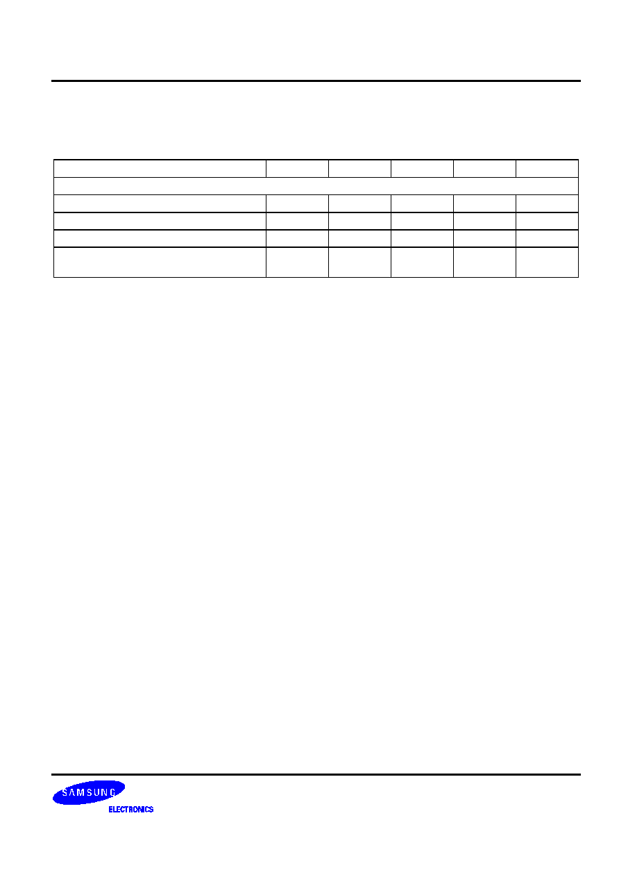
DIGITAL SPECIFICATIONS
(VDDA1=3.3V, VDDA2=3.3V, ADCCLK=20MHz, CDS1_CLK=6.666MHz, CDS2_CLK=6.666MHz, C
L
=20pF unless
otherwise noted)
Characteristics
Symbol
Min
Typ
Max
Unit
Comment
High
Level
Input
Voltage
V
IH
2.0
V
Low
Level
Input
Voltage
V
IL
0.7
V
High
Level
Input
Current
I
IH
10
uA
Low
Level
Input
Current
I
IL
10
uA
High
Level
Output
Voltage
V
oH
3.0
V
I
oH
= 0.5mA
Low
Level
Output
Voltage
V
OL
0.3
V
I
oL
= -0.5mA
TIMING SPECIFICATIONS
(VDDA1=3.3V, VDDA2=3.3V unless otherwise noted)
Characteristics
Symbol
Min
Typ
Max
Unit
CLOCK CHARACTERISTICS
3-Channel Conversion Rate
150
ns
1-Channel Conversion Rate
50
ns
CDSCLK1 Pulse Width
t
C1CLK
22
ns
CDSCLK2 Pulse Width
t
C2CLK
24
ns
CDSCLK2B Pulse Width
t
C2CLKB
24
ns
CDSCLK1 Falling to CDSCLK2 Rising
t
C1C2A
3
ns
CDSCLK2 Falling to CDSCLK1 Rising
t
C2C1A
3
ns
ADCCLK Pulse Width
t
ADCLK
22
ns
CDSCLK2 Rising to ADCCLK Rising
t
C2ADA
24
ns
CDSCLK2 Falling to ADCCLK Falling
t
C2ADB
3
ns
ADCCLK Rising to CDS2CLK Falling
t
ADC2A
3
ns
Aperture Delay
t
AD
2
ns
SERIAL INTERFACE
Maximum SCLK Frequency
f
CLK
10
MHz
SLOAD to SCLK Set-up Time
t
LS
10
ns
SCLK to SLOAD Hold Time
t
LH
10
ns
SDATA to SCLK Rising Set-up Time
t
DS
10
ns
SCLK Rising to SDATA Hold Time
t
DH
10
ns
SCLK Falling to SDATA Valid
t
RDV
10
ns
0.35
µ
µ
µ
µ
m 12-BIT 20MSPS AFE FOR CCD/CIS SIGNAL PROCESSOR
AFE1400X
7
TIMING SPECIFICATIONS
(VDDA1=3.3V, VDDA2=3.3V unless otherwise noted)
Characteristics
Symbol
Min
Typ
Max
Unit
DATA OUTPUT
ADC Output Delay
t
ADDT
10
ns
Tri-State to Data Valid
t
DEV
15
ns
Output Enable High to Tri-State
t
HZ
5
ns
ADC Latency(Pipeline Delay)
3
ADCCLK
Cycles
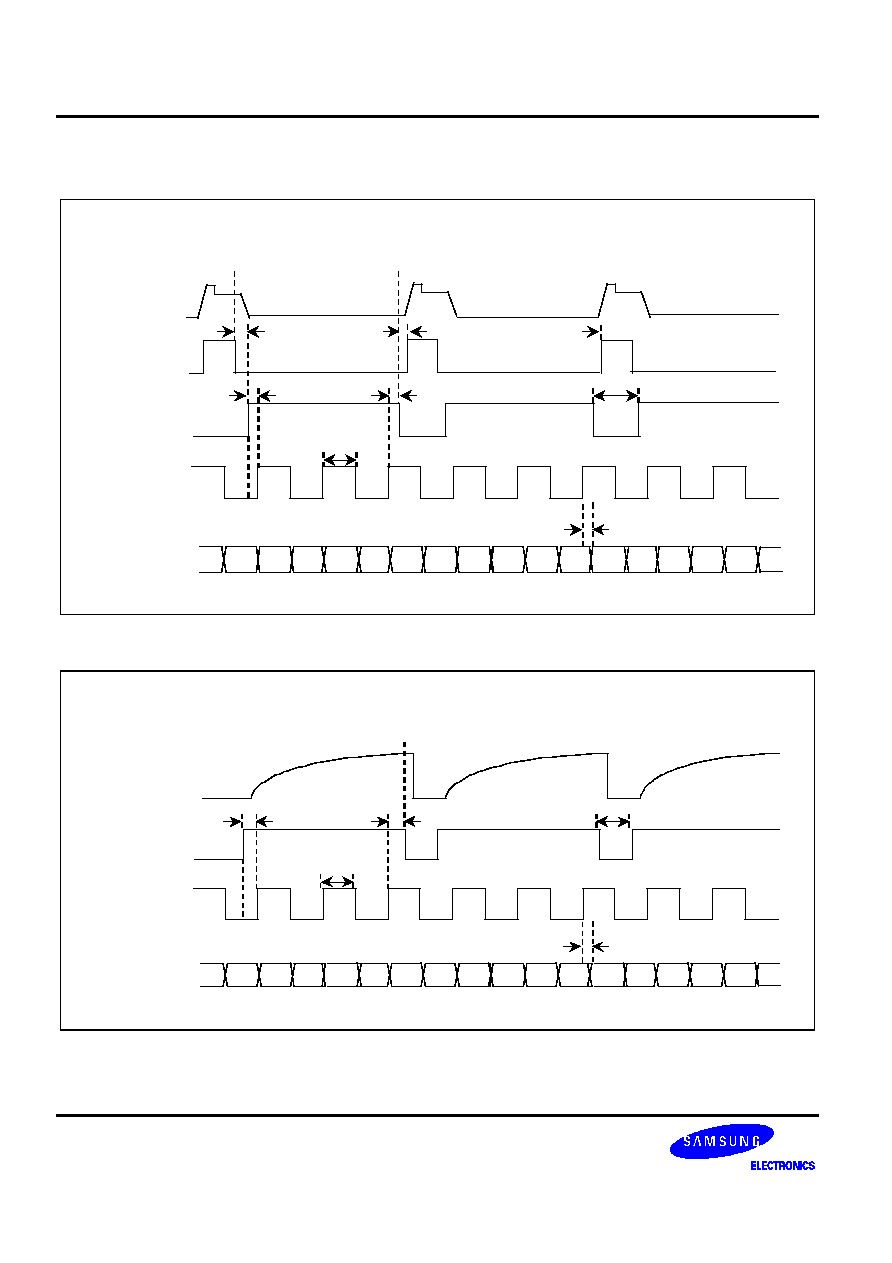
NOTE: Aperture
delay
is
a
timing
measurement
between
the
sampling
clocks
and
CDS.
It
is
measured
from
the
falling
edge
of
the
CDS2_CLK
input
to
when
the
input
signal
is
held
for
data
conversion
AFE1400X
0.35
µ
µ
µ
µ
m 12-BIT 20MSPS AFE FOR CCD/CIS SIGNAL PROCESSOR
8
TIMING
DIAGRAM
3-Channel CDS Mode
Analog
Input
CDS1_CLK
CDS2_CLK
ADCCLK
OUTPUT
D[7:0]
t
C1C2A
t
C2C1A
t
C1CLK
t
C2ADA
t
ADC2A
t
C2CLKB
t
ADCLK
R0,G0,B0
R1,G1,B1
R2,G2,B2
R-2 R-2 G-2 G-2 B-2 B-2 R-1 R-1 G-1 G-1 B-1 B-1 R0 R0 G0 G0 B0 B
t
ADDT
3-Channel SHA Mode
Analog
Input
CDS2_CLK
ADCCLK
R0,G0,B0
R1,G1,B1
R2,G2,B2
t
C2ADA
t
ADC2A
t
C2CLKB
t
ADCLK
OUTPUT
D[7:0]
R-2 R-2 G-2 G-2 B-2 B-2 R-1 R-1 G-1 G-1 B-1 B-1 R0 R0 G0 G0 B0 B
t
ADDT

0.35
µ
µ
µ
µ
m 12-BIT 20MSPS AFE FOR CCD/CIS SIGNAL PROCESSOR
AFE1400X
9
1-Channel CDS Mode
Analog
Input
CDS1_CLK
CDS2_CLK
ADCCLK
t
ADCLK
t
C2ADB
t
C2CLK
t
C1CLK
t
C2ADA
t
C1C2A
t
C2C1A
1-Channel SHA Mode
Analog
Input
CDS2_CLK
ADCCLK
R0,G0,B0
R1,G1,B1
R2,G2,B2
t
C2CLK
t
ADCLK
t
C2ADB
t
C2ADA

AFE1400X
0.35
µ
µ
µ
µ
m 12-BIT 20MSPS AFE FOR CCD/CIS SIGNAL PROCESSOR
10
Digital Output Data Timing
ADCCLK
OUTPUT
D[7:0]
Low
Byte
High Byte
D13-D6
D5-D0
Low
High
High
Low
t
ADDT
t
ADDT
t
HZ
t
DEV
OEB
Serial Write Operation Timing
SCLK
SDATA
R/Wb A2 A1 A0 XX XX XX D8 D7 D6 D5 D4 D3 D2 D1 D0
t
DS
t
DH
t
LS
t
LH
SLOAD
Serial Read Operation Timing
SCLK
SDATA
R/Wb A2 A1 A0 XX XX XX D8 D7 D6 D5 D4 D3 D2 D1 D0
t
DS
t
DH
t
LS
t
LH
SLOAD
t
RDV
'Read' means microcontroller reads SDATA.

0.35
µ
µ
µ
µ
m 12-BIT 20MSPS AFE FOR CCD/CIS SIGNAL PROCESSOR
AFE1400X
11
FUNCTIONAL
DESCRIPTION
1) 3-Channel Operation with CDS
This mode enables simultaneous sampling of a triple output CCD. The CCD waveforms are ac coupled to the
R_VIN, G_VIN and B_VIN pins where they are automatically biased at an appropriate voltage using the on-
chip clamp. The internal CDSs take two samples of the incoming pixel data; the first samples are taken during
the reset time while the second samples are taken during data portion of the input pixels.
2) 3-Channel SHA Operation
This mode enables simultaneous sampling of a triple output CIS or something like that. The CDS functions
are replaced with the sample and hold amplifiers. The input waveforms are either dc coupled or dc restored to
the R_VIN, G_VIN and B_VIN pins. The input reference voltage in this mode will be defined by external
OFFSET pin.
3) 1-Channel Operation with CDS
This mode enables single channel or monochrome sampling. The CCD waveforms are ac coupled to the
analog input pin where they are automatically biased at an appropriate voltage using the on-chip clamp.
Bit4, bit5 and bit6 in MUX register select the desired input among red, green and blue.
4) 1-Channel SHA Operation
This mode enables single-channel or monochrome sampling. The CDS function is replaced with the sample
and hold amplifier.
The input waveforms are either dc coupled or dc restored to the analog input pin. The input reference voltage
in this mode will be defined by clamp level control register.
Bit4, bit5 and bit6 in MUX register select the desired input among red, green and blue.

AFE1400X
0.35
µ
µ
µ
µ
m 12-BIT 20MSPS AFE FOR CCD/CIS SIGNAL PROCESSOR
12
MAIN BLOCK
DESCRIPTION
1) Programmable Gain Amplifier
The analog programmable gain can accommodate a wide range of input voltage spans. The transfer function
of the PGA is as follows.
H(X) = 1/12*X + 1,
where the range of X is 0 to 63.
Thus, the minimum gain value is equal to 1, and the maximum gain value is equal to 6.25. The transfer
function has linearity in linear scale. The overall gain is equal to analog gain multiplied by digital gain. So,
the multiplier should be required in back end of AFE.

0.35
µ
µ
µ
µ
m 12-BIT 20MSPS AFE FOR CCD/CIS SIGNAL PROCESSOR
AFE1400X
13
BLOCK
DIAGRAM
8
14
Input Offset
Register
(R,G,B)
CDS
PGA
12-bit
ADC
REF
PGA Gain
Register
(R,G,B)
Configuration
Register
R_VIN
RED
G_VIN
GREEN
B_VIN
BLUE
CDS1_CLK
CDS2_CLK
ADCCLK
OEB
SCLK
D[7:0]
OFFSET
MPU
PORT
VDDA1 VSSA1
VCOM
VDDA2 VSSA2
REFT
REFB
CDS
PGA
CDS
CLAMP
CLAMP
CLAMP
PGA
R_GAIN[5:0]
G_GAIN[5:0]
B_GAIN[5:0]
R_OFFSET[8:0]
G_OFFSET[8:0]
B_OFFSET[8:0]
R_OFFSET[8:0]
G_OFFSET[8:0]
B_OFFSET[8:0]
B_GAIN[5:0]
R_GAIN[5:0]
G_GAIN[5:0]
MUX
SDATA
VDDDR VSSDR
DAC
DAC
DAC
12:8
MUX
SLOAD

AFE1400X
0.35
µ
µ
µ
µ
m 12-BIT 20MSPS AFE FOR CCD/CIS SIGNAL PROCESSOR
14
2) INTERNAL REGISTER OVERVIEW
The internal register map is accessed through serial data pin SDATA's A0, A1 and A2.
Register Map
Register
Address
Data Bits
A2
A1
A0
D8
D7
D6
D5
D4
D3
D2
D1
D1
Configuration
0
0
0
0
0
0
3Ch/
1Ch
CDS
on
0
PWR
Dn
0
0
MUX
0
0
1
0
RGB/
BGR
Red
Green
Blue
0
0
0
0
Red PGA
0
1
0
0
0
0
MSB
LSB
Green PGA
0
1
1
0
0
0
MSB
LSB
Blue PGA
1
0
0
0
0
0
MSB
LSB
Red Offset
1
0
1
MSB
LSB
Green Offset
1
1
0
MSB
LSB
Blue Offset
1
1
1
MSB
LSB
Configuration Register
D8
D7
D6
D5
D4
D3
D2
D1
D0
Set to 0
1*
# of Channels
CDS Operation
1*
Power Down
Set to 0
X
1=3-CH mode*
0=1-CH mode
1=CDS Mode*
0=SHA Mode*
X
1=On
0=Off(Operation)*
NOTE: Power-on Default Value, X: Don't care
MUX Register
D8
D7
D6
D5
D4
D3
D2
D1
D0
Set to 0
3-CH Select
1-CH
1-CH
1-CH
Set to 0
1=R-G-B*
0=B-G-R
1=RED*
0=Off
1=Green
0=Off*
1=Blue
0=Off*
NOTE: Power-on Default Value

0.35
µ
µ
µ
µ
m 12-BIT 20MSPS AFE FOR CCD/CIS SIGNAL PROCESSOR
AFE1400X
15
PGA Gain Register
D8
D7
D6
D5
(MSB)
D4
D3
D2
D1
D0
(LSB)
Gain
(V/V)
Gain
(dB)
0*
0*
0*
0*
0*
0*
0*
0*
0*
1
0
0
0
0
0
0
0
0
0
1
1.083
0.693
0
0
0
0
0
0
0
1
0
1.167
1.341
. . .
0
0
0
1
1
1
1
1
0
6.167
15.801
0
0
0
1
1
1
1
1
1
6.25
15.918
NOTE: Power-on Default Value.
Offset Register
D8(MSB)
Sign Bit
D7
D6
D5
D4
D3
D2
D1
D0
(LSB)
Offset
(mV)
0*
0*
0*
0*
0*
0*
0*
0*
0*
0
0
0
0
0
0
0
0
0
1
0.781
0
0
0
0
0
0
0
1
0
1.563
. . .
0
1
1
1
1
1
1
1
1
200
1
0
0
0
0
0
0
0
0
-0.781
1
0
0
0
0
0
0
0
1
-1.563
. . .
1
1
1
1
1
1
1
1
1
-200
NOTE: Power-on Default Value.

AFE1400X
0.35
µ
µ
µ
µ
m 12-BIT 20MSPS AFE FOR CCD/CIS SIGNAL PROCESSOR
16
OVERALL TRANSFER
FUNCTION
The overall transfer function can be calculated as follows.
ADC
out
=[(Vin+Input_Offset)* PGA_Gain]/(2*REF)*4096,
where REF is equal to (REFT-REFB) and Input _Offset means the DAC value of the input offset register. The
analog offset range of the input offset register is varied between 200mV and -200 mV. The 9-bit data format for
the input offset register is sign magnitude, with D8 as the sign bit.
To maximize the dynamic range of the ADC input, it is necessary to program the input offset register code to
move the ADC code corresponding to the black level towards 'zero'.
And also PGA_gain is to maximize the dynamic range of the 12-bit ADC's input. The PGA_gain range is varied
between 1 and 6.25 by PGA gain register. The 6-bit data format for the PGA gain register is straight binary coding.
INPUT COUPLING
CAPACITOR
Because of the DC offset present at the output of CCD, some kind of DC restoration is required. In case of
CDS enable mode, to simplify input level shifting, a DC decoupling capacitor is used in conjuction with the
internal input circuitry.
The capacitor charging or discharging depends on the clamping time, the analog input resistance of the AFE and
the output resistance of the circuit driving the coupling capacitor.
The clamping time is typically (n*T), where n is the number of periods CDSCLK1 is asserted and T is the period
of assertion. CDSCLK2 should not be asserted during clamping time. The analog input resistance of the AFE's
Clamp is equal to 1 kW. The recommended input coupling capacitor is more than 0.1uF. The time constant of the
input clamp is determined by the internal 1K resistance and the external 0.1uF input capacitance. Thus, to extend
the clamping time, the time a transport motor moves the scanner carriage can be available, for example.

0.35
µ
µ
µ
µ
m 12-BIT 20MSPS AFE FOR CCD/CIS SIGNAL PROCESSOR
AFE1400X
17
POWER-ON
INITIALIZATION
Write to configuration register
Set CDS or SHA operation
Set 3 or 1 channel mode
Set color pointer
Set clamp mode
Write to PGA gain register
Set to gain of one(000000)
Write to input offset register
Set to 0mV(100000000)
Set another color
YES
NO

AFE1400X
0.35
µ
µ
µ
µ
m 12-BIT 20MSPS AFE FOR CCD/CIS SIGNAL PROCESSOR
18
CALIBRATION
Decide clamp level for SHA mode
(Refer to next page)
Set PGA gain
(Input offset = 0 mV)
Set another color
YES
NO
Scan dark line
Compute pixel offsets
Set input offset
Set odd/even offset in back end
Set gain/offset bus size
in back end
Set external pixel offset
in back end
Scan white line
Compute pixel gains
in back end
Adjust PGA gain
YES
NO
0.35
µ
µ
µ
µ
m 12-BIT 20MSPS AFE FOR CCD/CIS SIGNAL PROCESSOR
AFE1400X
19
CORE EVALUATION
GUIDE
0.1u
0.1u
0.1u
TIMING GENERATOR
MPU INTERFACE
DSP ASIC
MUX
MUX
Externally forced digital input/output
afe_cip4
ADCCLK
D[7:0]
REFT
SDATA
SCLK
SLOAD
CDS2_CLK
CDS1_CLK
G_VIN
B_VIN
R_VIN
VCOM REFB
AVDDA
AVSSA
AVDDD
AVSSD
AVBBA
OEB
OFFSET
AVBBD

AFE1400X
0.35
µ
µ
µ
µ
m 12-BIT 20MSPS AFE FOR CCD/CIS SIGNAL PROCESSOR
20
APPLICATIONS INFORMATION
CDS Mode Applications
-- The recommended input coupling capacitor value is 0.1uF.
-- A single ground plane is recommended for the afe_cip4. Thus the digital pins should be well decoupled to the
analog ground plane.
-- If possible, a separate power supply should be used for VDDDR, but this supply pin should still be decoupled
to the same ground plane as the rest of the afe_cip4.
-- The loading of digital outputs should be minimized.
-- All 0.1uF decoupling capacitors should be located as close as possible to the afe_cip4 pins.
-- When operating in single channel mode, the unused analog inputs must be grounded.
D7(MSB)
VSSDR
VDDDR
ADCCLK
CDSCLK
2
CDSCLK
1
OEB
D6
D1
D2
D3
D5
D4
D0(LSB)
B_VIN
VCOM
G_VIN
R_VIN
VSSA2
VDDA2
OFFSET
REFT
SCLK
SLOAD
VDDA1
REFB
VSSA1
SDATA
1
2
3
4
5
6
7
8
9
10
11
12
13
14
28
27
26
25
24
23
22
21
20
19
18
17
16
15
afe_cip4
0.01u
0.1u
0.01u
0.01u
0.1u 1.0u
0.1u
0.1u
10u
0.1u
0.1u
0.1u
0.1u
Data Outputs
3-Channel CDS Mode Application Circuit Configuration

0.35
µ
µ
µ
µ
m 12-BIT 20MSPS AFE FOR CCD/CIS SIGNAL PROCESSOR
AFE1400X
21
SHA Mode Applications
-- All of the CDS mode's considerations also apply for this configuration, except that analog inputs are directly
connected to the afe_cip4 without coupling capacitors.
-- The OFFSET pin may be used in a CIS application for DC offset adjustment. By connecting the appropriate dc
voltage to the OFFSET pin, the CIS signal will be restored to "zero".
3-Channel SHA Mode Application Circuit Configuration
D7(MSB)
VSSDR
VDDDR
ADCCLK
CDSCLK
2
CDSCLK
1
OEB
D6
D1
D2
D3
D5
D4
D0(LSB)
B_VIN
VCOM
G_VIN
R_VIN
VSSA2
VDDA2
OFFSET
REFT
SCLK
SLOAD
VDDA1
REFB
VSSA1
SDATA
1
2
3
4
5
6
7
8
9
10
11
12
13
14
28
27
26
25
24
23
22
21
20
19
18
17
16
15
afe_cip4
0.1u
0.1u
0.1u
10u
0.1u
0.1u
0.1u
0.1u
Data Outputs
AFE1400X
0.35
µ
µ
µ
µ
m 12-BIT 20MSPS AFE FOR CCD/CIS SIGNAL PROCESSOR
22
PACKAGE PIN
DESCRIPTION
Pin No.
Pin Name
I/O Type
Description
1
CDS1_CLK
DI
CDS Reference Sampling Clock
2
CDS2_CLK
DI
CDS Data Sampling Clock
3
ADCCLK
DI
A/D Converter Clock
4
OEB
DI
Output Enable (Active Low)
5
VDDDR
DP
Output Buffer Power
6
VSSDR
DG
Output Buffer Ground
7
D[7]
DO
Digital Output (MSB)
High Byte: D13, Low Byte: D5
8
D[6]
DO
Digital Output (D12, D4)
9
D[5]
DO
Digital Output (D11, D3)
10
D[4]
DO
Digital Output (D10, D2)
11
D[3]
DO
Digital Output (D9, D1)
12
D[2]
DO
Digital Output (D8, D0)
13
D[1]
DO
Digital Output (D7, X)
14
D[0]
DO
Digital Output (LSB)
High Byte: D6, Low Byte: X(Don't care)
15
SDATA
DB
Serial Interface Data Input/Output
16
SCLK
DI
Serial Interface Clock Input
17
SLOAD
DI
Serial Interface Load Pulse
18
VDDA1
AP
Analog Power
19
VSSA1
AG
Aanlog Ground
20
REFB
AB
Reference Decoupling
21
REFT
AB
Reference Decoupling
22
B_VIN
AI
Analog Input: Blue
23
VCOM
AB
Analog Common Voltage
24
G_VIN
AI
Analog Input: Green
25
OFFSET
AB
Clamp Bias Level Decoupling
26
R_VIN
AI
Analog Input: Red
27
VSSA2
DG
Digital Ground
28
VDDA2
DP
Digital Power
0.35
µ
µ
µ
µ
m 12-BIT 20MSPS AFE FOR CCD/CIS SIGNAL PROCESSOR
AFE1400X
23
USER GUIDE
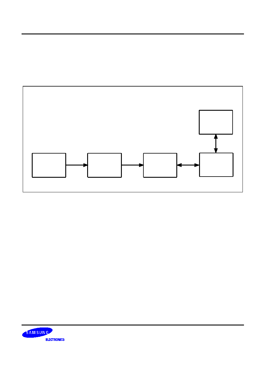
SYSTEM CONFIGURATION
It is necessary that output signal of analog front end be shading-compensated by back end logic block including
subtracter and multiplier.
(Shading-Compensation Block)
CCD/CIS
AFE
Subtracter
Multiplier
Controller
Memory
AFE1400X
0.35
µ
µ
µ
µ
m 12-BIT 20MSPS AFE FOR CCD/CIS SIGNAL PROCESSOR
24
QUESTIONNAIRE FOR ANALOG CORE
Characteristics
Symbol
Min
Typ
Max
Unit
Comment
Resolution
Bits
Signal-to-Noise & Distortion
Ratio
SNDR
dB
Conversion Rate
3-Channel with CDS
1-Channel with CDS
MSPS
MSPS
Differential
Nonlinearity
DNL
LSB
Integral
Nonlinearity
INL
LSB
Unipolar Offset Error
%FSR
Gain Error
%FSR
Anlog Input
Full-Scale Input
Vp-p
Power Supply
Analog Voltage
Digital Voltage
VDDA
VDDD
V
V
Power Consumption
mW
Temperature Range
∞
C
-- What do you want to choose as power supply voltages?
For example, the analog VDD needs to be 3.3V. The digital VDD can be 2.5V/3.3V.
-- Which modes of AFE do you use for overall system ? (Refer to page 9)
For example: 3channel operation with CDS / 3channel SHI(CIS) operation
1channel operation with CDS / 1channel SHI(CIS) operation
-- Would you define the gain range and input offset range ?
-- Could you explain external/internal pin configurations as required?
-- If possible, present other requirements below.

0.35
µ
µ
µ
µ
m 12-BIT 20MSPS AFE FOR CCD/CIS SIGNAL PROCESSOR
AFE1400X
25
HISTORY CARD
Version
Date
Modified Items
Comments
ver 1.0
2001.07
Original version published (preliminary)

AFE1400X
0.35
µ
µ
µ
µ
m 12-BIT 20MSPS AFE FOR CCD/CIS SIGNAL PROCESSOR
26
NOTES