
SEC ASIC
AL0402I
16Bit 44.1kHz Sigma-Delta Stereo DAC
ANALOG
DAC
&
Analog
Postfilter
Sinc Filter
&
Sigma-Delta
Modulator
Compensation
Filter
&
De-emphsis
&
FIR Filter
Anti-Imaging
Filter
Timing Generation
Voltage
Reference
S/P
Converter
&
Attenuator
SDATA
BCK
LRCK
ZDENL
AOUTL
VREF
IREF
AOUTR
I
D
N
U
M
<
7
:
0
>
F
S
E
L
<
1
:
0
>
M
L
D
M
D
A
T
A
M
C
L
K
MICOM Interface
D
E
E
M
D
N
M
S
C
K
R
S
T
B
B
I
S
T
O
N
P
M
U
T
E
L
P
D
L
T
S
E
L
I
A
D
S
R
I
A
D
S
L
I
F
S
6
4
O
D
S
R
O
D
S
L
O
F
S
6
4
S
D
I
A
G
S
E
R
R
O
R
B
General Description
This product is
Digital-To-Analog Converter for
digital audio System (CDP). The product contains
Serial-to-Parallel
Converter
and
Compensation
Filter, Digital Volume Attenuator by the MICOM
Interface, De-Emphasis Filter, FIR filter, Sinc Filter,
digital sigma-delta modulator, analog postfilter, AIF
(Anti-Image-Filter). The normal input and output
channels provides 95dB SNR (Signal to Noise
Ratio) over in band (20kHz).
The product employs the 1bit 4th-order sigma-delta
architecture with 16bit resolution, over sampling of
64X. And analog postfilter with low clock sensitivity
and linear phase, filters the shaping-nosie and
outputs analog voltage with high resolution. An
on-chip reference voltage is included to allow
single supply operations.
Features
-16bit
Digital-To-Analog Converter
-On-Chip Analog Postfilter
-Filtered Line-Level Outputs, Linear Phase Filtering
-On-Chip Voltage Reference
-95dB SNR
-Sampling Rate 32KHz/44.1kHz/48KHz
-Input Rate 1Fs or 2Fs by Normal Mode/Double
Mode Selection
-Zero Input Detection Mute
-On-Chip Compensation Filter
-Input Volume Attenuator by the MICOM Interface
-On-Chip De-Emphasis Filter
(32KHz/44.1KHz/48KHz)
-On-Chip 4 times oversampling Digital Filter
-Low Clock Jitter Sensitivity
-Single 5V Power Supply
Applications
CD Player, Portable CD Player, CD-ROM,
Video-CD, Mini-Disk, DVD etc
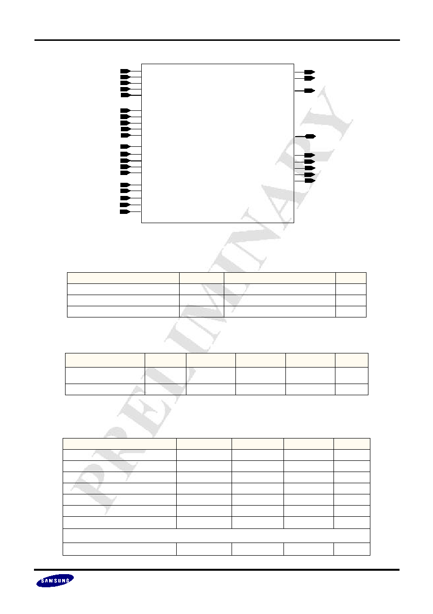
Block Diagram
Ver 1.0
(Nov 1999) This datasheet is a preliminary version. No responsibility is assumed by SEC for its
use nor for any infringements of patents or other rights of third parties that may result from its use. The
content of this datasheet is subject to change without any notice.
16Bit 44.1kHz Sigma-Delta Stereo DAC
AL0402I
VDDD VSSD
VBB
VDDA VSSA
1/10

SEC ASIC
AL0402I
16Bit 44.1kHz Sigma-Delta Stereo DAC
ANALOG
Embedded Core Block Diagram
Embedded Core User Guide
-
Digital serial data input and clock input refer to digital input format.
- Digital control pins inform refer to pin description.
- Micom I/F pin inform refer to micom interface. IDNUM<7:0> are ID number setting pins for micom
Interface.
- External application of analog output pins refer to application circuit.
- If you want to test only embedded analog core block (Sigma-Delta DAC), you can do it just adding the
4 pins to supply digital serial input data (LRCK, BCK, SDATA, MSCK) and MUX block.
- Analog power(VDDA,VSSA,VBB) and digital power(VDDD, VSSD) should be seperated.
- VBB pin should be connected to analog ground.
- Two pads should be dedicated to analog power(VDDA, VSSA)
- If you need not use test mode for the testability of internal core block, you make internal core block
test pins disable state. (Test Input pins are 'L' state and Test output, bidirection pins leave floating)
MSCK
BCK
LRCK
SDATA
AOUTL
VREF
AOUTR
ZDENL
DEEM
DN
MUTEL
PDL
RSTB
V
S
S
A
V
D
D
A
V
B
B
V
D
D
D
V
S
S
D
Audio Processor
(DSP)
al0402i
SDIAG
SERRORB
OFS64
ODSL
ODSR
BISTONP
TSEL
IFS64
IADSL
IADSR
MUX_SEL
External
Inputs
These are test pins for internal blocks of the core.
So you don't need the internal test mode.
Make the test control pins disable ('L') state and
Output and bidirectional pins leave foalting.
MCLK
MLD
MDATA
FSEL<1:0>
IDNUM<7:0>
M
U
X
4
4
4
IREF
VSSD
6
13
5
External
2/10

SEC ASIC
AL0402I
16Bit 44.1kHz Sigma-Delta Stereo DAC
ANALOG
Core Pin Description
SYMBOL
I/O TYPE
I/O PAD
DESCRIPTION
Power Supply Pins
VDDD
DP
vdd3t_bb
Digital Supply
VSSD
DG
vsst_bb
Digital Ground
VDDA
AP
vdd3t_bb
Analog Supply
VSSA
AG
vsst_bb
Analog Ground
Digital Pins
MSCK
DI
piccbb_bb
Master Clock Input. 384Fs Clock
BCK
DI
piccbb_bb
Bit Clock Input. (32Fs or 64Fs)
LRCK
DI
piccbb_bb
Sample Rate Clock Input. (Fs or 2Fs)
SDATA
DI
piccbb_bb
Serial Digital Input
MCLK
DI
piccbb_bb
Micom Interface Clock Input
MLD
DI
piccbb_bb
Micom Interface Command load Input (When low,load)
MDATA
DI
piccbb_bb
Micom Interface Command Data Input
DEEM
DI
piccbb_bb
De-Emphasis On/Off. "H" is enabled. "L" is disabled.
DN
DI
piccbb_bb
Input Rate Select. High is Double(2Fs) Mode, Low is Normal(Fs) Mode.
MUTEL
DI
piccbb_bb
Analog Output Mute. "L" enabled
ZDENL
DI
piccbb_bb
Zero Input Detection Enable. "L" is enabled. "H" is disabled
FSEL<1:0>
DI
piccbb_bb
De-Emphasis Sampling Frequency Mode Select
F S E L < 1 : 0 >
S a m p l i n g F r e q u e n c y
H
H
4 8 K H z
H
L
3 2 K H z
L
H
4 8 K H z
L
L
4 4 . 1 K H z
IDNUM<7:0>
DI
piccbb_bb
Micom Interface ID Number setting Input
PDL
DI
piccbb_bb
Power Down. "L" enabled
RSTB
DI
piccbb_bb
Reset Input. "L" Enabled
Analog Pins
AOUTL
AO
poabb_bb
Analog Output for L-CH
AOUTR
AO
poabb_bb
Analog Output for R-CH
VREF
AO
poabb_bb
Reference Voltage Output for Bypass
Core Internal Block Test Pins
BISTONP
DI
piccbb_bb
Memory Bist Test Mode. "H" enabled
TSEL
DI
piccbb_bb
Test pin for Analog Postfilter Input Selection
IFS64
DI
piccbb_bb
64X Sampling Clock Input for Analog Postfilter (When TSEL=H)
IADSL
DI
piccbb_bb
Inputs for Analog Postfilter of L-CH (When TSEL=H)
IADSR
DI
piccbb_bb
Inputs for Analog Postfilter of R-CH (When TSEL=H)
SDIAG
DO
pot2bb_bb
Test Output pin for embeded memory BIST (BIST_ON="H")
SERRORB
DO
pot2bb_bb
Test Output Pin for Embeded memory BIST (BIST_ON="H")
OFS64
DO
pot2bb_bb
64X Sampling Clock output for Digital sigma-delta Modulator
ODSL
DO
pot2bb_bb
L-CH Output for Digital sigma-delta Modulator.
ODSR
DO
pot2bb_bb
R-CH Output for Digital sigma-delta Modulator.
IREF
AB
poabb_bb
Test Pin for Analog Supply Current
I/O TYPE ABBR.
- AI : Analog Input
- DI : Digital Input
- AO : Analog Output
- DO : Digital Output
- AB : Analog Bidirectional
- DB : Digital Bidirectional
- AP : Analog Power
- AG : Analog Ground
- DP : Digital Power
- DG : Digital Ground
3/10
SEC ASIC
AL0402I
16Bit 44.1kHz Sigma-Delta Stereo DAC
ANALOG
Core Configurtion
Absolute Maximum Ratings
Characteristics
Symbol
Values
Unit
Supply Voltage
VDDD,VDDA
-0.3 ~ 7.0
V
Voltage on Any Digital Pin
Vin
VSSD-0.3 to VDDD+0.3
V
Storage Temperature Range
Tstg
-45 to +125
�
C
Recommended Operating Conditions
Charateristics
SYMBOL
MIN
TYP
MAX
UNITS
Supply Voltage
VDDD
VDDA
4.75
5.0
5.25
V
Operating Temp.
Topr
0
25
70
�
C
Electrical Characteristics
(VDDD,VDDA=5.0V, Temp=25
�
C, Fs=44.1kHz, Signal Frequency=20~20kHz, Cload of AoutL, AoutR=10pF)
PARAMETER
MIN
TYP
MAX
UNITS
Resolution
16
bits
SNR
<1>
90
95
dB
THD
<2>
0.004
0.007
%
SND(THD+Noise)
<3>
82
87
dB
Dynamic Range
<4>
85
90
dB
Reference Voltage Ouput
2.25
V
Frequency Responce
�
0.1
�
0.5
dB
Analog Output
Voltage Range
�
1.414
Vpp
al0402i
Used Power:
(VDDD VSSD VBB VDDA VSSA)
MSCK
BCK
LRCK
SDATA
ZDENL
MCLK
MLD
MDATA
FSEL<1:0>
IDNUM<7:0>
DEEM
DN
MUTEL
PDL
RSTB
BISTONP
TSEL
IFS64
IADSL
IADSR
AOUTL
AOUTR
VREF
IREF
SDIAG
SERRORB
OFS64
ODSL
ODSR
4/10

SEC ASIC
AL0402I
16Bit 44.1kHz Sigma-Delta Stereo DAC
ANALOG
Load Impedance
5K
Digital Filter
Pass Band Ripple
�
0.0072
dB
Stop Band Attenuation
62.7
dB
Pass Band
0.45
Fs
Power Supply
Analog Current
25
mA
Digital Current
20
mA
Power Dissipation
225
mW
Power Down Current
1
mA
<1> 1kHz 0dB Sinewave Input, EIAJ
<2> 1kHz 0dB Sinewave Input
<3> 1kHz 0dB Sinewave Input, (Not EIAJ)
<4> 1kHz -60dB Sinewve Input, and then measured data + 60dB
AC Timing Characteristics
(VDDD=5V, VSSD=0V, VBB = 0V, Temp=25
�
C, Sampling Frequency = 44.1kHz)
Characteristics
Symbol
Min
Typ
Max
Unit
MSCK Frequency
Fmck
-
16.9344
-
MHz
BCK Frequency (Normal/Doube Mode)
Fbck
1.4112 / 2.8224
(Normal / Double)
-
MHz
MSCK Rising and LRCK Edge Dealay
Tmld
0
-
-
ns
MSCK Risng and LRCK Edge Setup Time
Tmlst
10
-
-
ns
BCK Rising and LRCK Edge Dealay
Tbld
0
-
-
ns
BCK Risng and LRCK Edge Setup Time
Tblst
10
-
-
ns
SDATA and BCK Rising Setup Time
Tsbst
10
-
-
ns
BCK Ring and SDATA Hold Time
Tbsht
10
-
-
ns
5/10