 | –≠–ª–µ–∫—Ç—Ä–æ–Ω–Ω—ã–π –∫–æ–º–ø–æ–Ω–µ–Ω—Ç: al1211h | –°–∫–∞—á–∞—Ç—å:  PDF PDF  ZIP ZIP |
GENERAL
DESCRIPTION
The AL1211H is a CMOS 8-bit A/D converter for
video applications. It is a two-step ping-pong A/D
converter which consists of reference resistor-matrix,
4-bit coarse A/D converter and 4-bit fine A/D
converter.
The maximum conversion rate of AL1211H is 30MSPS
and supply voltage is 5V single.
TYPICAL
APPLICATIONS
°§Multi-media applications
°§Frame-grabber scanner
°§
Camcorder
°§Digital video (TV/VCR)
°§Broadcasting and studio equipments.
°§Medical Electronics (ultra-sound and imaging)
°§High speed instruments (Digital scope, radar)
FUNCTIONAL
BLOCK
DIAGRAM
FEATURES
°§
Resolution : 8Bit
°§
Differential Linearity Error : °æ1.0 LSB
°§
Integral Linearity Error : °æ1.0 LSB
°§
Maximum Conversion Rate : 30MSPS
°§
Sample & Hold Function Implemented
°§
Power Supply : 5V Single
8BIT 30MSPS ADC
AL1211H
Ver 1.1 (Feb. 2000)
No responsibility is assumed by SEC for its use nor for any
infringements of patents or other rights of third parties that may
result from its use. The content of this datasheet is subject to
change without any notice.
VIN
Fine
Sampling
Amplifier
Fine
Sampling
Amplifier
Analog
Mux
Latch
Reference
Matrix
Coarse
Sampling
Amplifier
Latch
Encoder
Encoder
Error
Correction
Circuit
Timing Generator
Data
Latches
and
3-state
Output
Buffer
VDD
VSSA
VDDA
VRT
CLK
Latch
COUT
FOUT
FREF
VSS
VRB
DO<0> (LSB)
DO<7> (MSB)
DO<1>
DO<2>
DO<3>
DO<4>
DO<5>
DO<6>

AL1211H
8BIT 30MSPS ADC
SEC ASIC
ANALOG
CORE
PIN
DESCRIPTION
NAME
I/O TYPE
I/O PAD
PIN DESCRIPTION
VRT
DB
pia_bb
2.6V External Reference Top Bias
VRB
DB
pia_bb
0.6V External Reference Bottom Bias
VIN
AI
pia_bb
Analog Input
Input Span : VRB ~ VRT
CLK
DI
picc_bb
Clock Input
D<7:0>
DO
pot2_bb
Digital Output
VDDA
AP
vdda
Analog Power
VSSA
AG
vssa
Analog Ground
VDD
DP
vdd3
Digital Power
VSS
DG
vssd
Digital Ground
CORE
CONFIGURATION
I/O TYPE ABBR.
°§AI : Analog Input
°§DI : Digital Input
°§AO : Analog Output
°§DO : Digital Output
°§AB : Analog Bidirectional
°§DB : Digital Bidirectional
°§AP : Analog Power
°§
DP : Digital Power
°§
AG : Analog Ground
°§
DG : Digital Ground
°§AB : Analog Bidirection
°§DB : Digital Bidirection
VIN
D<7:0>
VRT
VRB
al1211h
VDDA VSSA
VDD
VSS
VIN
CLK
D<7:0>
VRT
VRB
al1211h
VDDA VSSA
VDD
VSS
2 / 11

AL1211H
8BIT 30MSPS ADC
SEC ASIC
ANALOG
ABSOLUTE
MAXIMUM
RATINGS
NOTES
1. ABSOLUTE MAXIMUM RATING specifies the values beyond which the device may be damaged permanently.
Exposure to ABSOLUTE MAXIMUM RATING conditions for extended periods may affect reliability. Each
condition value is applied with the other values kept within the following operating conditions and function
operation under any of these conditions is not implied.
2. All voltages are measured with respect to VSS unless otherwise specified.
3. 100pF capacitor is discharged through a 1.5ß⁄ resistor (Human body model)
RECOMMENDED
OPERATING
CONDITIONS
NOTES
1. It is strongly recommended that all the supply pins (VDDA, VDD) be powered from the same source to avoid
power latch-up.
Characteristic
Symbol
Value
Unit
Supply Voltage
VDD
7.0
V
Analog Input Voltage
VIN
-0.3 to VDD+0.3
V
Digital Input Voltage
CLK
-0.3 to VDD+0.3
V
Digital Output Voltage
V
OH
, V
OL
-0.3 to VDD+0.3
V
Reference Voltage
VRT/VRB
-0.3 to VDD+0.3
V
Storage Temperature Range
Tstg
-40 to 125
°…
Operating Temperature Range
Topr
0 to 70
°…
Characteristics
Symbol
Min
Typ
Max
Unit
Supply Voltage
VDDA - VSSA
VDD - VSS
4.75
5
5.25
V
Supply Voltage Difference
VDDA - VDD
-0.1
0.0
0.1
V
Reference Input Voltage
VRT
VRB
-
-
2.6
0.6
-
-
V
Analog Input Voltage
AIN
VRB
-
VRT
V
Clock High Time
Clock Low Time
Tpwh
Tpwl
-
-
16.6
16.6
-
-
ns
Digital Input 'L' Voltage
Digital Input 'H' Voltage
V
IL
V
IH
-
4.5
-
-
0.5
-
V
Operating Temperature
Topr
0
-
70
°…
3 / 11

AL1211H
8BIT 30MSPS ADC
SEC ASIC
ANALOG
DC
ELECTRICAL
CHARACTERISTICS
AC ELECTRICAL
CHARACTERISTICS
Characteristics
Symbol
Min
Typ
Max
Unit
Conditions
Resolution
-
8
-
-
Bits
-
Reference Current
IREF
7
10.5
11
mA
VRT : 2.6V
VRB : 0.6V
Differential Linearity Error
DLE
°æ
0.2
°æ
0.3
°æ
1.0
LSB
VIN : 0.6 ~ 2.6V
(sine wave 4Mhz)
Integral Linearity Error
ILE
°æ0.2
°æ0.5
°æ1.0
LSB
Fs : 1MHz
20MHz
Bottom Offset Voltage Error
EOB
-
-
2.5
LSB
EOB = VIN(0,1) - VRB
Top Offset Voltage Error
EOT
-
-
* 15
LSB
EOT = VRT - VIN(254,255)
Characteristics
Symbol
Min
Typ
Max
Unit
Conditions
Conversion Rate
Fs
30
-
-
MSPS
VIN : 4MHz
(Sine Input)
Dynamic Supply Current
Is
15
23
30
mA
Is = I(VDDA) + I(VDDD)
Fs : 30MHz
Digital Output Data Delay
Td
-
5
10
ns
* Td is Core internal delay
See
"DELAY TIMING DIAGRAM"
Signal to Noise Ratio
SNR
40
43
-
dB
VIN : 4MHz (Sine Input)
Fs : 30MHz
NOTES
1. Converter Specifications (unless otherwise specified)
VDDA=5V
VDD=5V
VSSA=GND
VSS=GND
VRT=2.6V
VRB=0.6V
Ta=25°…
* EOT has large value because of long routing between PAD and VRT. Top offset voltage error can be reduced to
25mV by modifying layout
4 / 11
AL1211H
8BIT 30MSPS ADC
SEC ASIC
ANALOG
DELAY
TIMING
DIAGRAM
VIN
CLK
DO
DO (-2)
A1
A2
A3
A4
td
DO (-1)
DO (0)
DO (1)
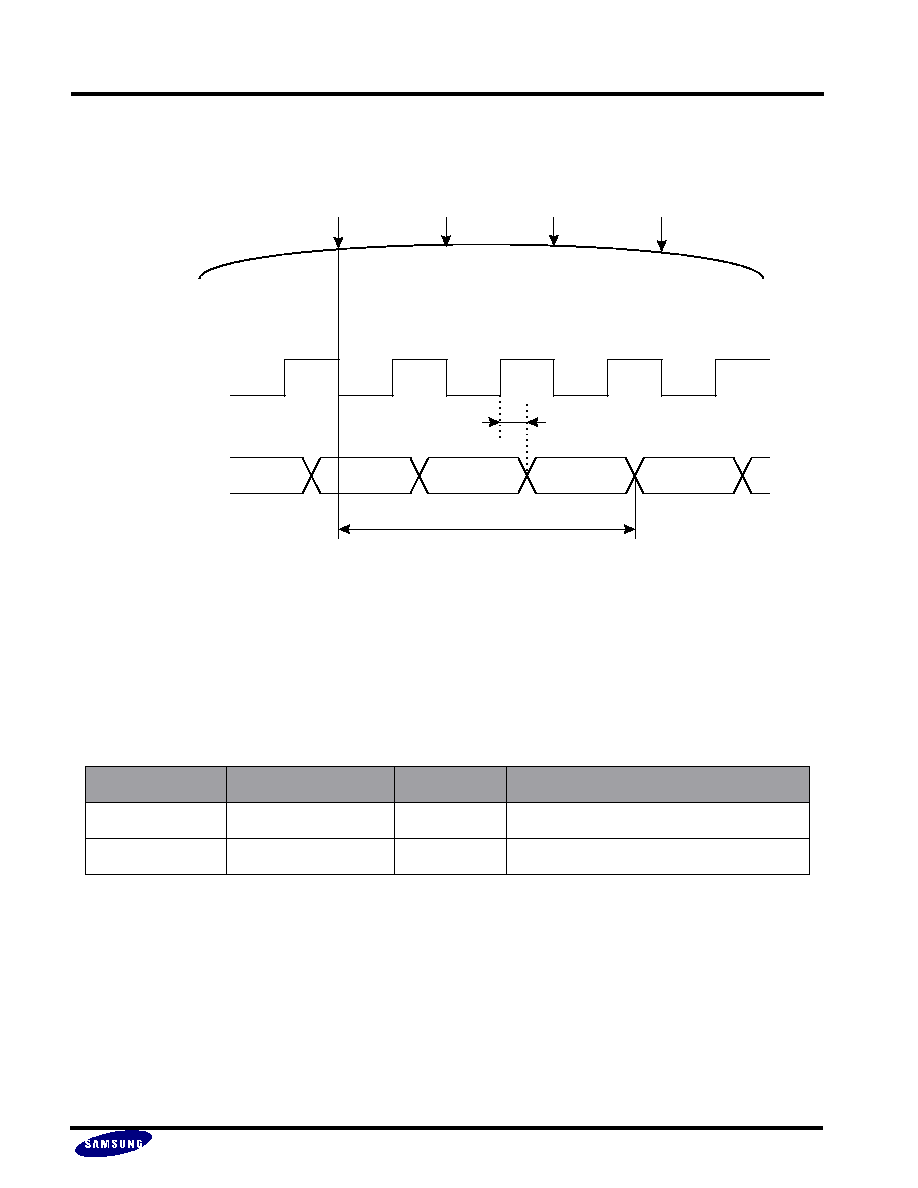
2.5 CLK PIPELINE DELAY
Patameter
Limit
Units
Conditions/Comments
Td
10
ns
Output Data Delay Time
Tpd
2.5°øCLK
ns
Pipe lined delay
TIMING
SPECIFICATION
5 / 11

AL1211H
8BIT 30MSPS ADC
SEC ASIC
ANALOG
FUNCTIONAL
DESCRIPTION
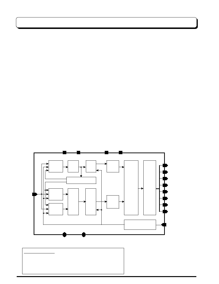
1. AL1211H is two-step ping-pong A/D converter
with subranging reference resistor matrix.
It consists of 4-bit coarse A/D converter and fine
A/D converter whose resolution is 4.459 bits
approximately.
The
latching
comparators
in
coarse and fine A/D converters have offset
cancellation features built in such as auto-zero
and averaging, and the number of comparators
are 15 in the coarse converter and 42 in the
fine.
The sampling operation of fine A/D converter is
performed, through 21 analog MUXs, in a
ping-pong manner between its two sampling
amplifier banks each of which consists of 21
latching comparators.
2. One of 16 different sets of reference voltages
are switched, according to the states of the
coarse comparators, to the fine sampling amplifier
banks by the reference resistor matrix. This fact
and the use of a CMOS auto-zero comparator
surely eliminate the extra pain for implementing
high accuracy D/A converter of 8 bit or more,
and thus a low-power, high-performance and high
speed A/D converter follows.
3. The operation of AL1211H can be stated as
follows. (refer to the 'TIMING DIAGRAM' that
follows)
During the first cycle of external clock the
analog input 'VIN' is traced by each converter,
and at the falling edge of CLK 'VIN' is sampled
and held to be compared with the 16-level coarse
reference voltages. The result of comparison in
coarse
comparator,
'COUT',
is
latched and
chooses a set of fine reference voltage 'FREF'
which, to be compared with the sampled analog
input, is fed to the fine sampling amplifier banks.
The result of the comparison is reproduced by
successive comparators with sufficiently large
gain and then multiplexed to the latching digital
logics in a ping-pong manner. Latching logics in
coarse and fine converters refine the results of
comparison to generate A/D converter output
'FOUT' and 'COUT'
and from which the final
digital output 'DOUT' results.
The overall pipeline delay, measured from the
sampling instance to the time that the 'DO'
comes to be available, is 2.5 clock cycles.
4. AL1211H implements the correction scheme to
correct the error which stems from the mismatch
between the offset of coarse A/D converter and
that of the fine A/D converter. This scheme can
handle a error of up to 3LSBs and helps
reducing
the
differential
linearity
error
consequently.
6 / 11

AL1211H
8BIT 30MSPS ADC
SEC ASIC
ANALOG
TIMING
DIAGRAM
VIN
C1T
CSamp
C2T
CComp
FREF
COUT
C1T1
FSamp1
C2T1
FComp1
C2T2
FComp2
C1T2
FSamp2
MUX
OUT
FOUT
DATA
A1
A2
A3
A4
A5
A0
A2
A3
A4
A0
A1
A2
A3
FComp1
FComp2
FComp2
FComp1
FComp1
A0
A1
A2
A3
A0
A1
A2
2.5 Clock Pipeline Delay
A1
7 / 11
AL1211H
8BIT 30MSPS ADC
SEC ASIC
ANALOG
CORE
EVALUATION
GUIDE
1. ADC function is evaluated by external check on the bidirectional pads connected to input nodes of
HOST DSP back-end circuit.
2. The reference voltages may be biased externally through VRT and VRB pins
MUX
BI
D
IRECTIONAL PAD
ADC Func
tion
M
easuring
&
D
igital Input
Forc
ing
HOST
DSP
CORE
VIN
CLK
D<7:0>
VRT
VRB
al1211h
2.6
V
Top
Reference
0.6
V
Botto
m
Reference
VDDA
VSSA
VDD
VSS
GND
+5V
Ana
log Po
wer
GND
+5V
D
igital Po
wer
: 0.1uF CERA
M
IC CAPACITOR
UNLESS OTHER
W
ISE SPECIFIED
NOTES
: 10uF CERA
M
IC CAPACITOR
UNLESS OTHER
W
ISE SPECIFIED
8 / 11

AL1211H
8BIT 30MSPS ADC
SEC ASIC
ANALOG
CORE LAYOUT GUIDE
DDA
Fine
COMP
VDD
RMATRIX
NWELL Guardring
P+ Guardring
DO<0> ~ DO<7>
Digtal Output
Coarse
COMP
* It is recommended that you use thick VDDA,VSSA ,VRT, VRB Pin. when connecting to PAD, the path should
be kept as short as possible.
* Digital power and analog power are separately used.
* When P+ Guardring and NWELL Guarding are connected to other blocks, it must be double shielded using
N-well and P+ active to remove the substrate and coupling noise. In that case, the power metal should be connected
to PAD directly.
CKGEN
SSA
CLK
VRB
VRT
FROM
CROM
CRORRECT
VSS
VIN
VBB
9 / 11

AL1211H
8BIT 30MSPS ADC
SEC ASIC
ANALOG
PACKAGE
CONFIGURATION
NOTES
1. You can test ADC function by checking external bidirectional pad connected to internal signal path.
2. ESD (ElectroStatic Discharge) sensitive device. Although the digital control inputs are diode protected, permanent
damage may occur on devices subjected to high electrostatic discharges. It is recommended that unused devices be
stored in conductive foam or shunts to avoid performance degradation or loss of functionality. The protective foam
should be discharged to the destination socket before devices are inserted.
3. NC denotes "No Connection".
1
2
3
4
5
6
7
8
9
10
11
12
13
14
15
16
17
18
19
20
21
22
23
24
48
47
46
45
44
43
42
41
40
39
38
37
36
35
34
33
32
31
30
29
28
27
26
25
NC
VRT
VRB
NC
NC
NC
NC
NC
NC
NC
NC
NC
NC
NC
V D D A
VSSA
VIN
NC
NC
V D D O B
VSSOB
CLK
NC
NC
NC
D < 7>
D < 6>
D < 5>
D < 4>
D < 3>
D < 2>
D < 1>
D < 0>
VSS
V D D
AL1211H
NC
NC
NC
NC
NC
NC
NC
NC
NC
NC
NC
NC
NC
0.1u
47u
47u
0.1u
47u
0.1u
47u
0.1u
47u
0.1u
D
igi
ta
l Ou
tput
Analog Input
Clock Signal
Ref Top
Ref Bottom
I/O PAD Power
D igital Pow e r
Analog Pow e r
10 / 11

AL1211H
8BIT 30MSPS ADC
SEC ASIC
ANALOG
ADC Specification
Parameter
Min
Typ
Max
Unit
Remarks
Supply voltage
V
Reference Input voltage
V
Analog Input voltage
Vpp
Operating temperature
°…
Integral non-linearity error
LSB
Differential non-linearity
error
LSB
Offset voltage error
(Bottom)
mV
Offset voltage error
(Top)
mV
Maximum conversion rate
MSPS
Dynamic supply current
mA
Power dissipation
mW
Signal-to-noise ratio
dB
Digital output format
(Provide detailed
description & timing
diagram)
- What do you want to choose as power supply voltages? For example, the analog VDD needs
to be 5V. the digital VDD can be 3.3V/5V.
- What resolution do you need for ADC?
- How about the conversion speed(data in°Êdata out)?
- How many cycles do exist during the latency of ADC (pipelined delay)?
- What's the input range? And what do you need between the single input and differential
input?
- Can the bus interface be compatible with TTL?
- Could you explain external/internal pin configurations as required?
Specially requested function list :
We appreciate your interest in our products. If you have further questions, please specify in
the attached form. Thank you very much.
11 / 11