 | –≠–ª–µ–∫—Ç—Ä–æ–Ω–Ω—ã–π –∫–æ–º–ø–æ–Ω–µ–Ω—Ç: al1212h | –°–∫–∞—á–∞—Ç—å:  PDF PDF  ZIP ZIP |
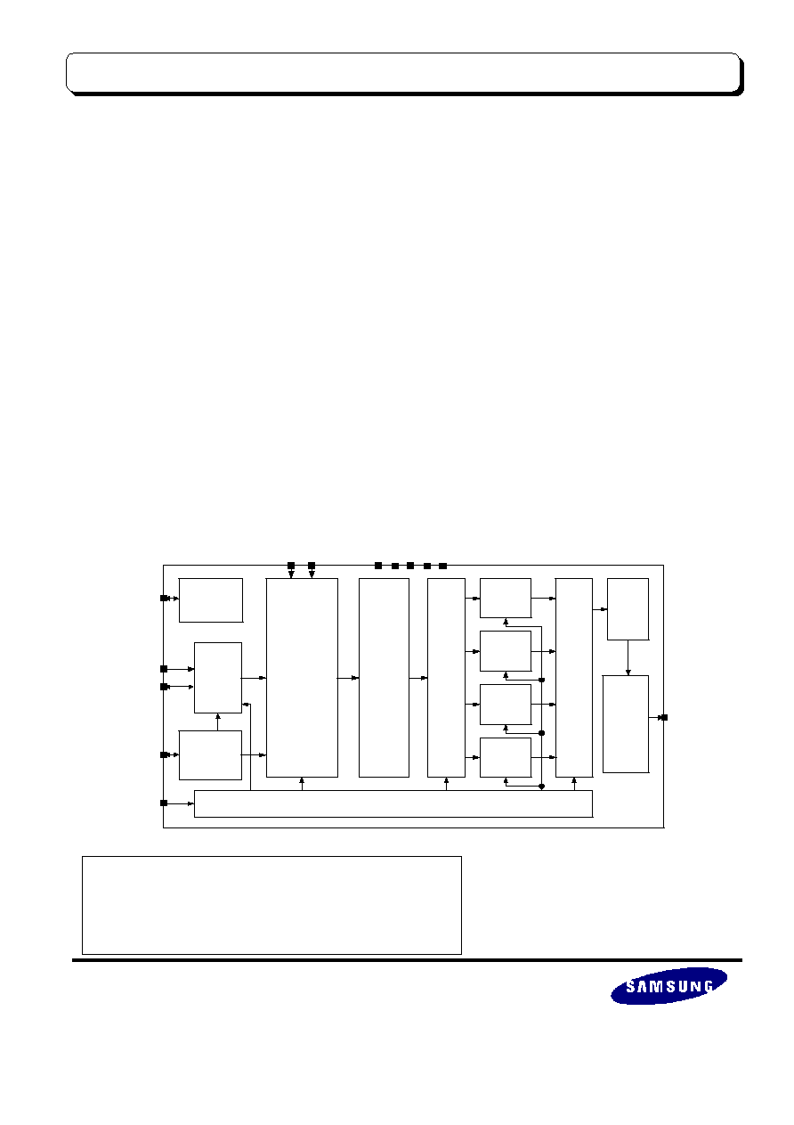
FUNCTIONAL BLOCK DIAGRAM
GENERAL DESCRIPTION
The AL1212H is a CMOS 6-Bit A/D converter for a
digital video disk (DVD) partial-response maximum
likelihood (PRML) system.
It is a flash type A/D
converter which consists of input buffer, comparator
array, digital backend encoder, and output buffer.
The
maximum
conversion
rate
of
AL1212H
is
over
120MSPS and supply voltage is 5V single.
TYPICAL APPLICATIONS
- Multi-media applications
- Digital video disk (DVD) system
- Digital broadcast satellite (DBS) receiver
- Quadrature phase shift keying (QPSK) demodulator
- Video applications
FEATURES
- Resolution : 6Bit
- Differential Linearity Error : ±1.0 LSB
- Integral Linearity Error : ±1.0 LSB
- Maximum Conversion Rate : 120MSPS
- Digital Output : CMOS Level
- Power Consumption : 300mW
- Power Supply : 5V Single
4-bit
ROM
Block
DSL
Block
Input
Buffer
CML
Level
Generator
Clock Generator
FNAND
Array
Comparator
Array
Flip/
Flop
Array
Output
Buffer
Bias
Current
Generator
AINT
4-bit
ROM
Block
4-bit
ROM
Block
4-bit
ROM
Block
CLKIN
Flip/
Flop
Array
INCOM
REFTOP
REFBOT
DO[9:0]
ITEST
CML
VDDA
VSSA
VBBA
VDDD
VSSD
6BIT 120MSPS ADC
AL1212H
SAMSUNG ELECTRONICS Co. LTD
Ver 1.0 (Mar. 1999)
No responsibility is assumed by SEC for its use nor for any
infringements of patents or other rights of third parties that may
result from its use. The content of this datasheet is subject to
change without any notice.

SEC ASIC
AL1212H
6BIT 120MSPS ADC
ANALOG
CORE PIN DESCRIPTION
NAME
I/O TYPE I/O PAD
PIN DESCRIPTION
REFTOP
AI
pia_bb
Reference Top Bias (3.0V)
REFBOT
AI
pia_bb
Reference Bottom Bias (2.0V)
CML
AB
pia_bb
Internal Bias Point
(open=use internal bias circuit)
VDDA
AP
vdda
Analog Power (5.0V)
VBBA
AG
vbba
Analog Sub Bias
VSSA
AG
vssa
Analog Ground
AINT
AI
piar10_bb
Analog Input
Input Span : 1.5~3.5 V
INCOM
AB
pia_bb
Internal Bias Point
(open=use internal bias circuit)
ITEST
AB
pia_bb
Internal Bias Point
(open=use internal bias circuit)
CLKIN
DI
piar50_bb
Clock Input
DO[5:0]
DO
poa_bb
Digital Output
VSSD
DG
vssd
Digital Ground
VDDD
DP
vddd
Digital Power (5.0V)
CORE CONFIGURATION
I/O TYPE ABBR.
- AI : Analog Input
- DI : Digital Input
- AO : Analog Output
- DO : Digital Output
- AB : Analog Bidirectional
- DB : Digital Bidirectional
- AP : Analog Power
- DP : Digital Power
- AG : Analog Ground
- DG : Digital Ground
AINT
CLKIN
DO[5:0]
al1212h
REFTOP
REFBOT
CML
INCOM
ITEST
VDDA
VSSA
VBBA
VDDD
VSSD
2 / 11

SEC ASIC
AL1212H
6BIT 120MSPS ADC
ANALOG
ABSOLUTE MAXIMUM RATINGS
Characteristics
Symbol
Value
Unit
Supply Voltage
VDD
7.0
V
Analog Input Voltage
AINT
VSS to VDD
V
Digital Input Voltage
CLKIN
VSS to VDD
V
Digital Output Voltage
V
OH
, V
OL
VSS to VDD
V
Reference Voltage
REFTOP/REFBOT 3.0/2.0
V
Storage Temperature Range
Tstg
-45 to 125
∫C
NOTES
1. ABSOLUTE MAXIMUM RATING specifies the values beyond which the device may be damaged permanently.
Exposure to ABSOLUTE MAXIMUM RATING conditions for extended periods may affect reliability. Each condition
value is applied with the other values kept within the following operating conditions and function operation under any
of these conditions is not implied.
2. All voltages are measured with respect to VSS unless otherwise specified.
3. 100pF capacitor is discharged through a 1.5K
resistor (Human body model).
RECOMMENDED OPERATING CONDITIONS
Characteristics
Symbol
Min
Typ
Max
Unit
Supply Voltage
VDDA - VSSA
VDDD - VSSD
4.5
5.0
5.5
V
Supply Voltage Difference
VDDA - VDDD
-0.1
0.0
0.1
V
Reference Input Voltage
REFTOP
REFBOT
-
-
3.0
2.0
-
-
V
Analog Input Voltage
AINT
1.5
-
3.5
V
Digital Input 'L' Voltage
Digital Input 'H' Voltage
V
IL
V
IH
-
4.5
-
-
0.5
-
V
Operating Temperature
Topr
0
-
70
∫C
NOTES
1. It is strongly recommended that all the supply pins (VDDA, VDDD, VDDO) be powered from the same source to avoid
power latch-up.
3 / 11

SEC ASIC
AL1212H
6BIT 120MSPS ADC
ANALOG
DC ELECTRICAL CHARACTERISTICS
Characteristics
Symbol
Min
Typ
Max
Unit
Conditions
Resolution
-
-
6
-
Bits
-
Reference Current
IREF
-
0.8
-
mA
REFTOP : 3.0V
REFBOT : 2.0V
Differential Linearity Error
DLE
-
-
±1.0
LSB
AINT : 1.5V ~ 3.5V
(Ramp Input)
Integral Linearity Error
ILE
-
-
±1.0
LSB
Fs : 120MHz
Bottom Offset Voltage Error
EOB
-
1
3
LSB
EOB = AINT(0,1)-REFBOT
Top Offset Voltage Error
EOT
-
1
3
LSB
EOT = REFTOP-AINT(62,63)
NOTES
1. Converter Specifications (unless otherwise specified)
VDDA=5.0V
VDDD=5.0V
SUBST=0.0V
VSSA=.0.0V
VSSD=0.0V
REFTOP=3.0V REFBOT=2.0V
Ta=25∫C
2. TBD : To Be Determined
AC ELECTRICAL CHARACTERISTICS
Characteristics
Symbol
Min
Typ
Max
Unit
Conditions
Conversion Rate
Fs
-
120
-
MSPS
Dynamic Supply Current
Is
(IREF)
-
60
(0.8)
66
mA
Is = I(VDDA) + I(VDDD)
Fs : 120MHz
Digital Output Data Delay
td
-
1.1
-
ns
See
"DELAY TIMING DIAGRAM"
Signal to Noise Ratio
SNDR
32
34
-
dB
AINT : 20MHz (Sine Input)
Fs : 120MHz
4 / 11

SEC ASIC
AL1212H
6BIT 120MSPS ADC
ANALOG
DELAY TIMING DIAGRAM
AINT
CLKIN
DO
DO (-1)
AIN(1)
AIN(2)
AIN(3)
td
DO (0)
DO (1)
DO (2)
Signal Delay
5 / 11

SEC ASIC
AL1212H
6BIT 120MSPS ADC
ANALOG
FUNCTIONAL DESCRIPTION
1. AL1212H is a flash A/D converter, which
consists of input buffer, comparator array, digital
backend encoder, and clock generator.
2. The input buffer is used to reduce a relatively
large input capacitance of the A/D converter and
convert single-ended input to differential output,
which is provided to comparator array.
3. Comparator array generates a thermometer code
from analog input and reference levels.
As it
has an interpolation factor of 2, this architecture
halves the number of preamplifiers but maintains
the same number of latches without extra
capacitors and resistors.
Each preamplifier
amplifies the analog input with performing an
auto-zero function simultaneously.
Each latch
converts analog output of the preamplifier into
fully
digital
signal
by
positive
feedback
operation.
4. The digital backend part composed of logic gates
and ROM blocks converts the comparator outputs
into 6-bit binary-coded digital words.
The
FNAND array, which converts a thermometer
code of the comparators into a single HIGH
level output, consists of 3-input NAND gates for
sparkle code suppression.
The digital backend
encoding block consists of four 4-bit ROMs to
achieve fast encoding, low power consumption,
and small digital area.
Each FROM block
encodes 16-bit input code into 4-bit LSB and
generates extra 1-bit, named a group selection bit
(GSB), which becomes HIGH when the 4-bit
output code is valid. DSL block, which consists
of some logic gates, generates 2-bit MSB from
the 4-bit GSBs.
To prevent timing errors, the
digital backend part contains two stage flip/flop
arrays which synchronize propagated signals with
the external clock.
5 Clock generator consists of analog clock generator
and digital clock generator.
Analog clock
generator generates approximately 1 MHz low
frequency
clocks,
which
are
supplied
to
preamplifiers and input buffer while digital clock
generator generates a 120 MHz high frequency
clock, which is supplied to latches and digital
backend encoder.
6 / 11

SEC ASIC
AL1212H
6BIT 120MSPS ADC
ANALOG
CORE EVALUATION GUIDE
1. ADC function is evaluated by external check on the bidirectional pads connected to input nodes of HOST
DSP back-end circuit.
2. The reference voltages should be biased externally through REFTOP and REFBOT pins.
AINT
CLKIN
DO[5:0]
al1212h
REFTOP
3.0V
Top
Reference
VSSA
REFBOT
2.0V
Bottom
Reference
VSSA
ITEST
CML
INCOM
UNLESS OTHERWISE SPECIFIED
: 10uF CERAMIC CAPACITOR
UNLESS OTHERWISE SPECIFIED
NOTES
UNLESS OTHERWISE SPECIFIED
: 0.1uF CERAMIC CAPACITOR
: 1nF CERAMIC CAPACITOR
ANALOG
MUX
HOST
DSP
CORE
BIDIRECTIONAL PAD
ADC Function
Measuring
&
Digital Input
Forcing
6-bit
Digital
Output
Analog
Input
Clock
Input
VBBA
VDDA
VSSA
VSSA
VSSD
VDDD
VSSD
5.0V
5.0V
7 / 11

SEC ASIC
AL1212H
6BIT 120MSPS ADC
ANALOG
CORE LAYOUT GUIDE
1. The width of all signal and power lines, which are connected to the ports of AL1212H block, must be
same to one of the connected ports.
2. The power lines, which have over 20um width, may be designed by the slit form.
3. Each power line, which has same label, must be tied in front of the I/O pad block.
4. Analog signal lines (AINT, REFTOP, REFBOT, CML, INCOM, and ITEST) must be separated to the
digital lines (CLKIN and DO[5:0]).
5. The lines of AINT and CLKIN may be designed as a straight line and maintain an enough space (over
10um) with other lines as it possible.
8 / 11

SEC ASIC
AL1212H
6BIT 120MSPS ADC
ANALOG
PACKAGE CONFIGURATION
NOTES
1. NC denotes "No Connection".
1
2
3
4
5
6
7
8
9
10
11
12
13
14
15
16
17
18
19
20
21
22
23
24
REFTOP
REFBOT
REFTOP
REFBOT
CML
VDDA
VDDA
VBBA
VSSA
VSSA
AINT
NC
INCOM
NC
NC
ITEST
NC
VSSO
VDDO
CLKIN
NC
NC
NC
NC
al1212h_top
48
47
46
45
44
43
42
41
40
39
38
37
36
35
34
33
32
31
30
29
28
27
26
25
VDDD
VSSD
VDDD
VSSD
NC
NC
NC
NC
DO[5]
DO[4]
DO[3]
DO[2]
DO[1]
DO[0]
NC
NC
NC
NC
NC
NC
NC
NC
NC
NC
2.0V
3.0V
1n
1n
10u
10u
5.0V
1n
0.1u
1K
50
0.1u
0.1u
0.1u
5.0V
1n
10u
50
5.0V
1n
0.1u
6-b ADC
output
Analog
input
Clock in
: Test Pin
No bias forcing, Remain floating
0.1u
0.1u
0.1u
10u
0.1u
10u
9 / 11

SEC ASIC
AL1212H
6BIT 120MSPS ADC
ANALOG
PACKAGE PIN DESCRIPTION
NAME
PIN NO.
I/O TYPE
PIN DESCRIPTION
REFTOP
1,2
AI
Reference Top (3V)
REFBOT
3,4
AI
Reference Bottom (2V)
CML
5
AB
Internal Bias Point (Open=use internal bias circuit)
VDDA
6, 7
AP
Analog Power (5V)
VBBA
8
AG
Analog Sub Bias
VSSA
9, 10
AG
Analog Ground
AINT
11
AI
Analog Input +
INCOM
13
AB
Analog Input - (Open=use internal bias circuit)
ITEST
16
AB
Internal Bias Point (Open=use internal bias circuit)
VDDO
18
PP
Output Driving Power
VSSO
19
PG
Output Driving Ground
CLKIN
20
DI
Clock Input
DO[5:0]
35~40
DO
Digital Output
VSSD
45,46
DG
Digital Ground
VDDD
47,48
DP
Digital Power
NOTES
1. I/O TYPE PP and PG denote PAD Power and PAD Ground respectively.
2. INCOM is the other pin of differential input, which is fixed to 2.5 V internally.
3. CML is the bias pin, which is fixed to 2.5 V internally.
4. ITEST is the test pin of bias generator. When initial bias function is working normally the pin is fixed to 0.9 V.
5. VDDO and VSSO are output driving power pads.
10 / 11

SEC ASIC
AL1212H
6BIT 120MSPS ADC
ANALOG
FEEDBACK REQUEST
It should be quite helpful to our ADC core development if you specify your system requirements on ADC in
the following characteristic checking table and fill out the additional questions.
We appreciate your interest in our products. Thank you very much.
Characteristic
Min
Typ
Max
Unit
Remarks
Analog Power Supply Voltage
V
Digital Power Supply Voltage
V
Bit Resolution
Bit
Reference Input Voltage
V
Analog Input Voltage
Vpp
Analog Input Bandwidth
(Maximum Input Frequency)
MHz
Operating Temperature
∫C
Integral Non-linearity Error
LSB
Differential Non-linearity Error
LSB
Bottom Offset Voltage Error
mV
Top Offset Voltage Error
mV
Maximum Conversion Rate
MSPS
Dynamic Supply Current
mA
Power Dissipation
mW
Signal-to-noise Ratio
dB
Pipeline Delay
CLK
Output Loading Capacitance
pF
Digital Output Format
(Provide detailed description &
timing diagram)
1. Between single input-output and differential input-output configurations, which one is suitable for your
system and why?
2. Please comment on the internal/external pin configurations you want our ADC to have, if you have any
reason to prefer some type of configuration.
3. Freely list those functions you want to be implemented in our ADC, if you have any.
11 / 11