 | ÐлекÑÑоннÑй компоненÑ: al1213a | СкаÑаÑÑ:  PDF PDF  ZIP ZIP |
AL1213A.PDF
AL1213A
8-BIT 0.5MSPS DAC
1
GENERAL DESCRIPTION
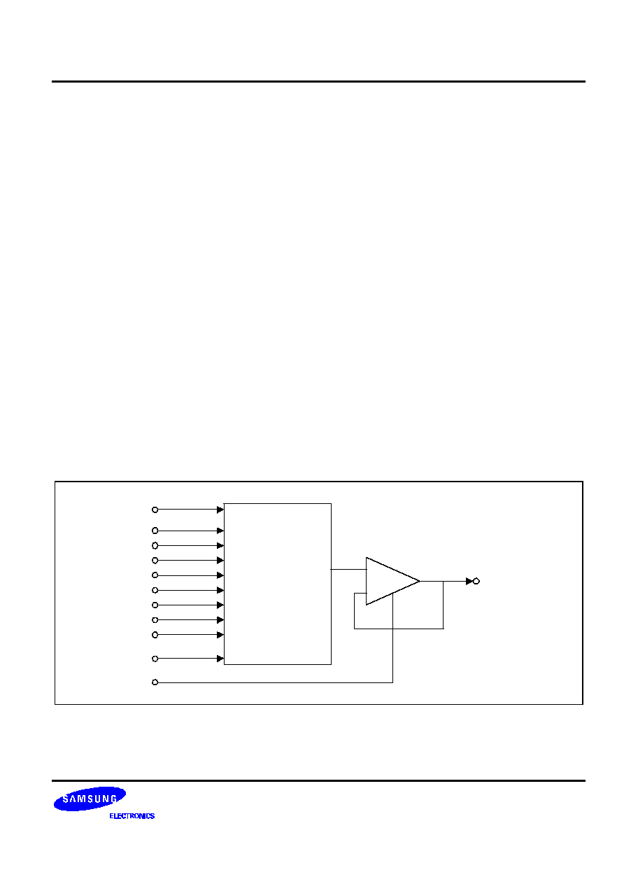
The AL1213A is a CMOS 8-bit D/A converter for general application. This digital to analog converter consists of a
R-2R ladder block & an Op amp block. Its maximum conversion rate is 0.5MSPS.
FEATURES
·
Resolution : 8-bit
·
Differential Linearity Error :
±
0.4 LSB (TYP)
·
Maximum Conversion Rate : 0.5MSPS
·
Supply Voltage : 5V
·
External Voltage Reference
·
Single Voltage Output : 0V to 5V
·
Operation Temperature Range : 0 to 70
°
C
TYPICAL APPLICATIONS
·
DVD
·
CDP
·
General purpose Digital to Analog Conversion
FUNCTIONAL BLOCK DIAGRAM
D[6]
VOUT
D[7]
D[2]
D[3]
D[4]
D[5]
D[0]
D[1]
VRB
VRT
PD
R2R
LADDER
OP
AMP
Rev 2.1 (Apr. 2002)
No responsibility is assumed by SEC for its use nor for any infringements of patents or other rights of third parties
that may result from its use. The content of this datasheet is subject to change without any notice.
8-BIT 0.5MSPS DAC
AL1213A
2
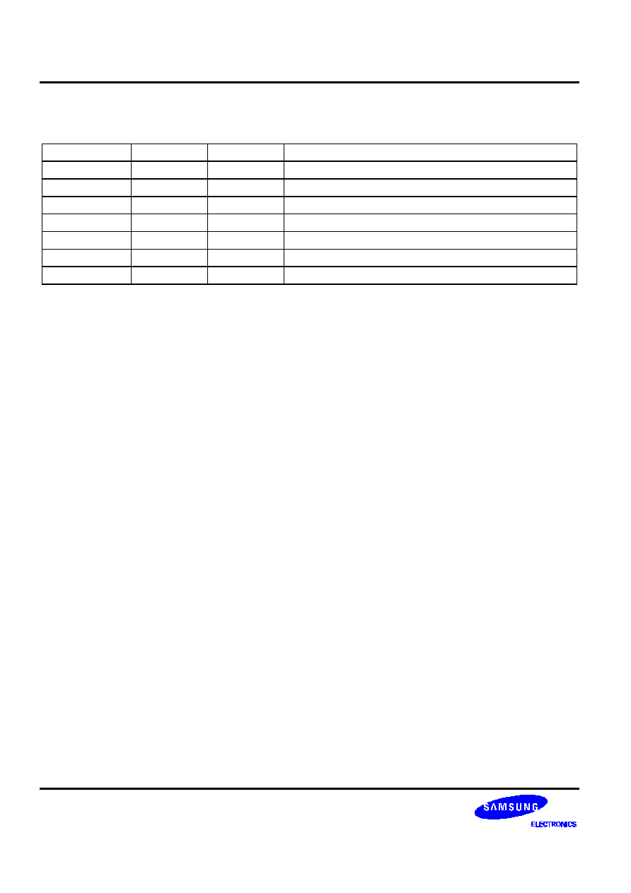
CORE PIN DESCRIPTION
Name
I/O Type
I/O Pad
Pin Description
DI0 ~ DI7
DI
picc_bb
Digital Input Data
VRB
AI
pia_bb
Voltage Reference Bottom (0V)
VRT
AI
pia_bb
Voltage Reference Top (5V)
AOUT
AO
poa_bb
Analog Voltage Output
VDDA
AP
vdda
Analog Power
VSSA
AG
vssa
Analog Ground
VBB
AG
vbb
Analog Ground
I/O TYPE ABBR
·
AI : Analog Input
·
DI : Digital Input
·
AO : Analog Output
·
DO : Digital Output
·
AP : Analog Power
·
AG : Analog Ground
·
AB : Analog bi-direction port
·
DB : Digital Bidirection port
·
DP : Digital Power
·
DG : Digital Ground
·
DB : Digital Sub Bias
AL1213A
8-BIT 0.5MSPS DAC
3
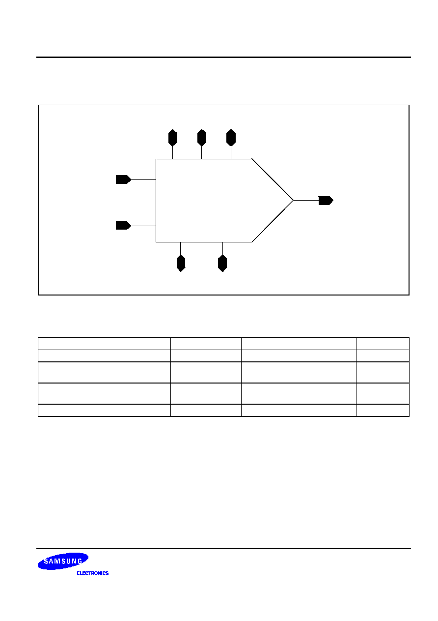
CORE CONFIGURATION
al1213a
D[7:0]
VOUT
VSSA
VDDA
VBB
VRT
VRB
PD
ABSOLUTE MAXIMUM RATINGS
Characteristics
Symbol
Typ
Unit
Supply Voltage
VDDA
5
V
Reference Input Voltage
VRT
VRB
5.0
0.0
V
V
Digital Input Voltage HIGH
LOW
Vinh
Vinl
5.0
0.0
V
V
Operating Temperature
Top
0 to 70
°
C
NOTES
:
1.
ABSOLUTE
MAXIMUM
RATING
specifies
the
values
beyond
which
the
device
may
be
damaged
permanently.
Exposure
to
ABSOLUTE
MAXIMUM
RATINGS
conditions
for
extended
periods
may
affect
reliability.
Each condition
value
is
applied
with
the
other
values
kept
within
the
following
operating
conditions
and
function
operation
under
any
of
these
conditions
not
implied.
2.
All
voltages
are
measured
with
respect
to
VSSA, VDDD
unless
otherwise
specified.
8-BIT 0.5MSPS DAC
AL1213A
4
RECOMMENDED OPERATING CONDITIONS
Characteristics
Symbol
Min
Typ
Max
Unit
Supply Voltage
VDDA
4.75
5.0
5.25
V
Reference Input Voltage
VRT
VRB
-
-
5.0
0.0
-
-
V
V
Digital Input Voltage HIGH
LOW
Vinh
Vinl
0.7 VDDD
-
-
-
-
0.3 VDDD
V
V
Operating Temperature
Top
0
-
70
°
C
NOTE: It is strongly recommended that to avoid power latch-up all the supply pins (VDDA, VDDD) be driven from the
same source.
DC ELECTRICAL CHARACTERISTICS
(Converter Specifications : VDDA = 5V, VSSA = VBB = 0V, Top = 25
°
C, VRT = 5.0V, VRB = 0.0V Cload = 2pF
unless otherwise specified.)
Characteristics
Symbol
Min
Typ
Max
Unit
Resolution
-
-
8
-
Bits
Differential Linearity Error
DLE
-
0.4
±
1
LSB
Integral Linearity Error
ILE
-
0.8
±
1
LSB
Maximum Output Voltage
-
4.75
5
5.25
V
LSB Size
-
19.0
19.5
20
mV
AL1213A
8-BIT 0.5MSPS DAC
5
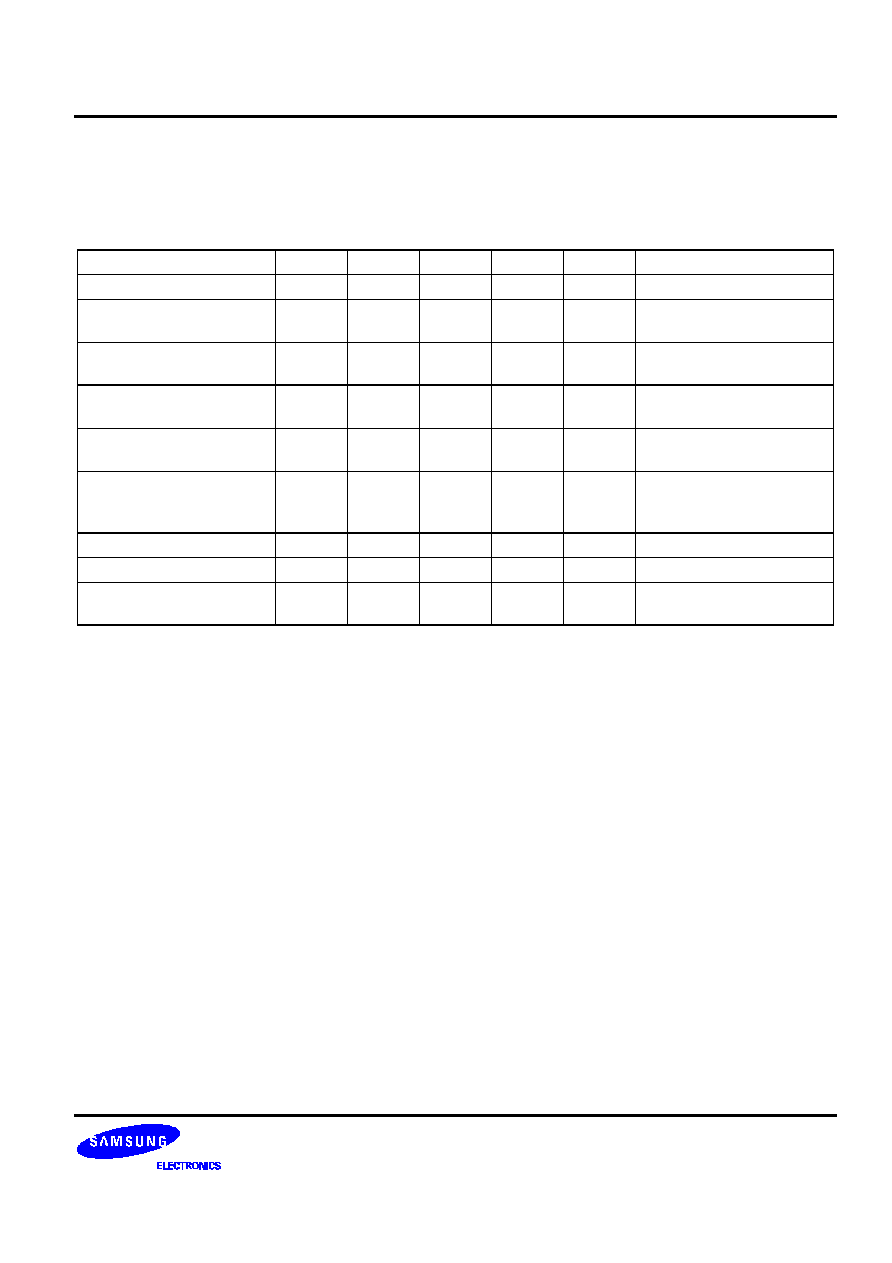
AC ELECTRICAL CHARACTERISTICS
(Converter Specifications : VDDA = 5V, VSSA = VBB = 0V, Top = 25
°
C, VRT = 5.0V, VRB = 0.0V Cload = 2pF
unless otherwise specified.)
Characteristics
Symbol
Min
Typ
Max
Unit
Test Conditions
Conversion Rate
fc
-
0.5
-
MSPS
data = 0.5MHz
Dynamic Supply Current
Ivdd
1.5
2.3
7.0
mA
fc = 0.5MHz
(load cap = 25pF)
Analog Output Delay
Td
-
190
270
ns
fc = 0.5MHz
Data : All High
Analog Output Rise Time
Tr
-
230
300
ns
fc = 0.5MHz
Data : All Low
All High
Analog Output Fall Time
Tf
-
230
300
ns
fc = 0.5MHz
Data : All High
All Low
Center Code Rising Time
Trd
-
0.3
0.4
ms
fc = 0.5MHz
Data :
01111111
10000000
Power down on time
Tpon
-
30
-
ns
Data : 11111111
Power down off time
Tpof
-
240
-
ns
Data : 11111111
Power down current
Ipd
-
4
50
nA
Data : 11111111
PD : 0V
8-BIT 0.5MSPS DAC
AL1213A
6
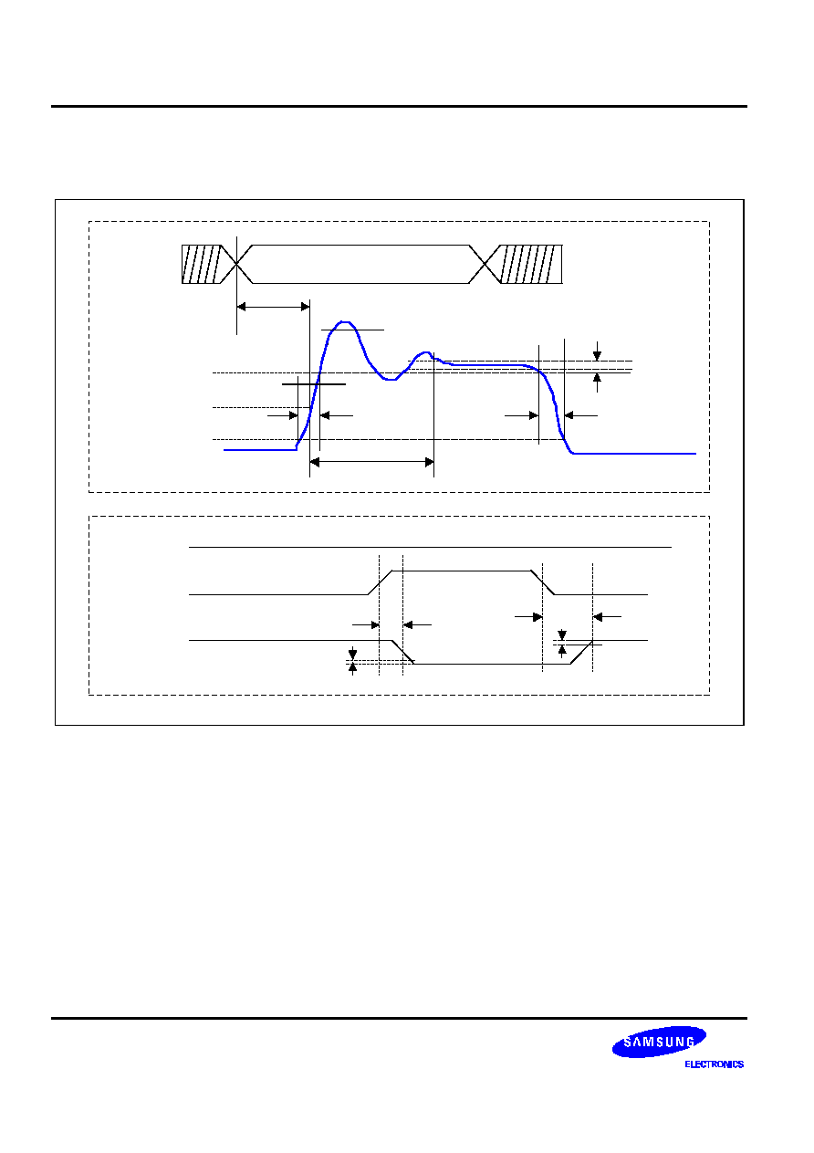
TIMING DIAGRAM
D[0]-D[7]
DATA
VOUT
Td
Ts
Tr
Tf
1LSB
D[0]-D[7]
PD
VOUT
90%
50%
10%
Tpon
Tpof
+/- 1/2LSB
+/- 1/2LSB
1. Output delay measured from the 50% point of the rising edge of input data to the full scale transition.
2. Settling time measured from the 50% point of full scale transition to the output remaining within
±
1/2 LSB.
3. Output rise/fall time measured between the 10% and 90% points of full scale transition.
FUNCTION DESCRIPTION
1.
The AL1213A has a R-2R Ladder Block for 8bit and an Opamp Block for driving Output.
2.
The R-2R Ladder Block generates binary weighted voltage (VRT/2
1
VRT/2
2
VRT/2
3
. . . VRT/2
n
)
corresponding to Digital Input Data for n-bit DAC and Output total voltage is summing of each values.
3.
In Output voltage, MSB = VRT/21 LSB = VRT/2n
4.
Output of the R2R Ladder Block is driven by Opamp
AL1213A
8-BIT 0.5MSPS DAC
7
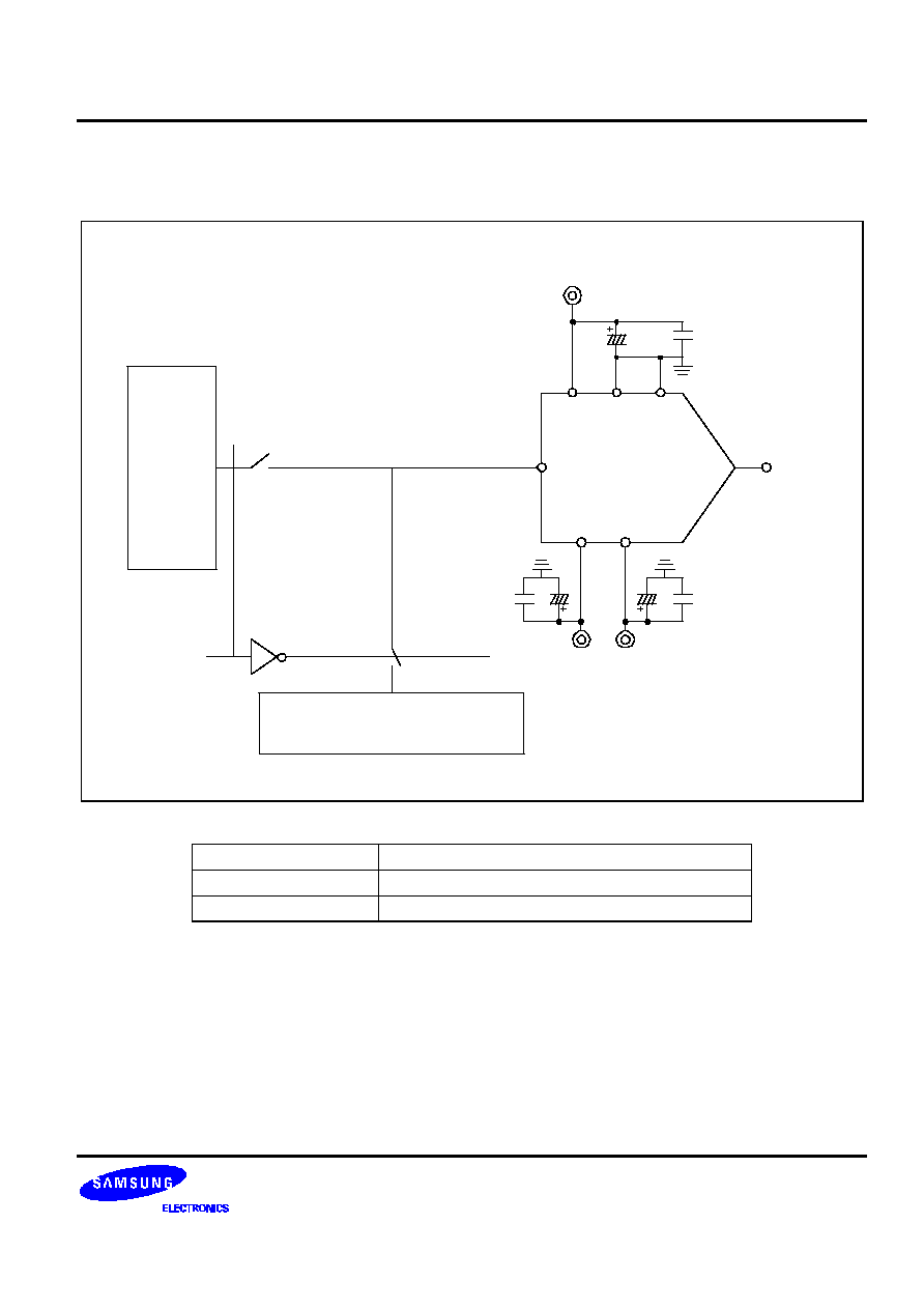
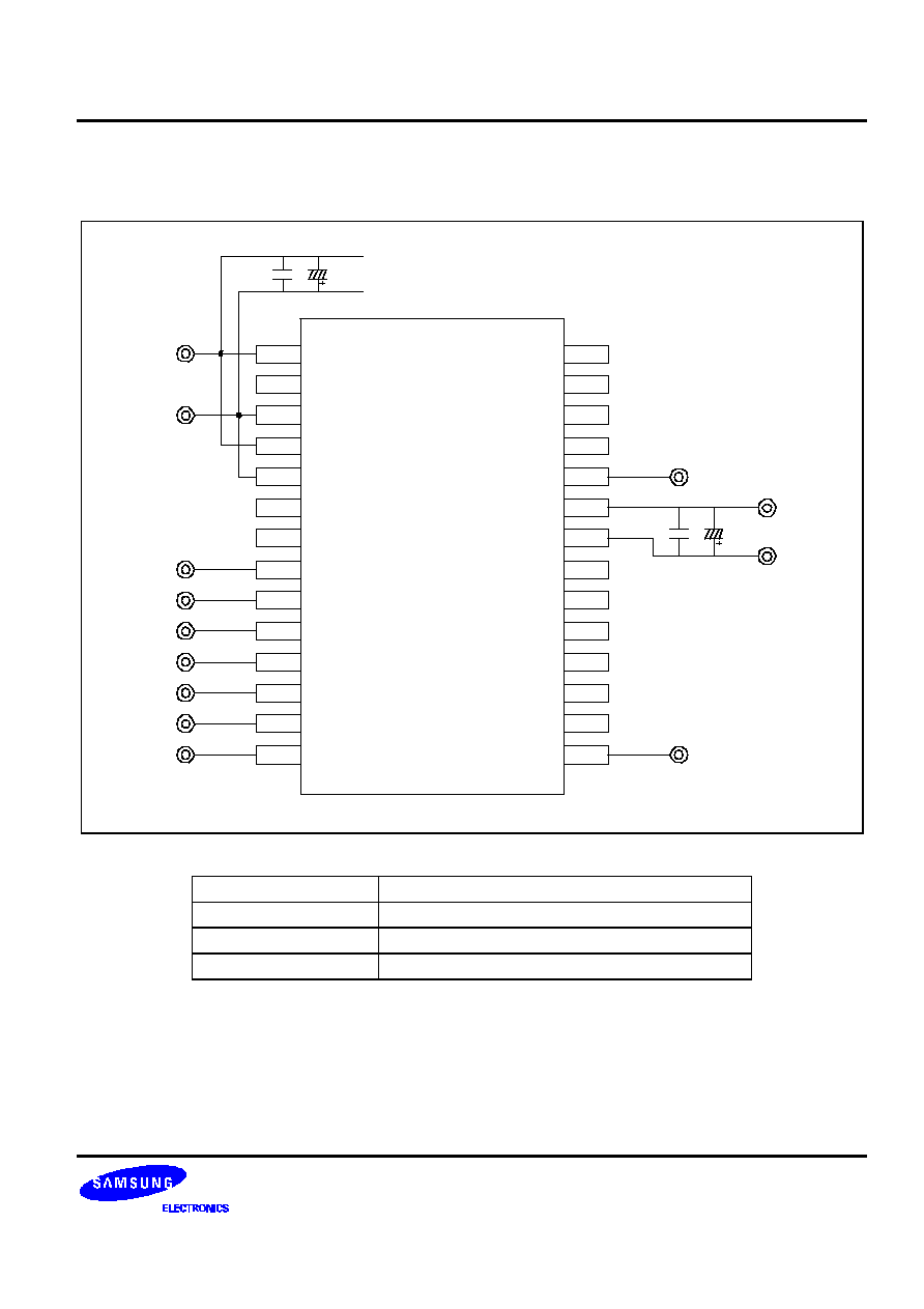
CORE EVALUATION GUIDE
VOUT
SELECT
D[7:0]
al1213a
VRT
VRB
VDDA VSSA
VBB
5V
Ct
Cc
MAIN PATH
TEST PATH
Ct
Cc
Ct
Cc
5V
0V
Location
Description
Ct
10mF TANTALUM CAPACITOR
Cc
0.1mF CERAMIC CAPACITOR
8-BIT 0.5MSPS DAC
AL1213A
8
TESTABILITY
Whether you use MUX or the internal logic for testability, it is required to be able to select the values of digital
inputs (D[0] ~ D[7]). See above figure. Only if it is, you can check the main function (Linearity)
PHANTOM CELL INFORMATION
VOUT
AL1213A
VRT
VRB
D[0]
D[1]
D[2]
D[3]
D[4]
D[5]
D[6]
D[7]
PD
VSSA
VBB
VDDA
Pin Name
Property
Pin Usage
Pin Layout Guide
D[7:0]
DI
Internal / External
1. Digital Input Signal lines must have same length to
PD
DI
Internal / External
reduce propagation delay.
VRT
AB
Internal / External
1. Voltage reference lines (VRT / VRB) must be wide metal
to reduce voltage drop of metal lines
VRB
AB
Internal / External
2. VOUT signal should not be crossed by any signals and
should not run next to digital signals to minimize capacitive
VOUT
AO
Internal / External
coupling between the two signals.
VDDA
AP
External
1. It is recommended that you use thick analog power
metal.
VSSA
AG
External
When connected to PAD, the path should be kept as short
VBB
AG
External
as possible.
1.
When the core block is connected to other blocks, it must be double guard-ring using N-well and
P+ active to remove the substrate and coupling noise.
In that case, the power metal should be connected to PAD directly.
2. The Bulk power is used to reduce the influence of substrate noise.
AL1213A
8-BIT 0.5MSPS DAC
9
PACKAGE CONFIGURATION
AL1213A
VSSA
NC
D[7]
D[6]
D[5]
D[4]
D[3]
D[2]
NC
NC
NC
NC
VRB
VRT
AOUT
D[1]
VDDA
NC
VBB
VDDA
NC
NC
NC
NC
NC
NC
D[0]
VOUT
D[1]
D[2]
D[3]
D[4]
D[5]
D[6]
D[7]
NC
D[0]
1
2
3
4
5
6
7
8
9
10
11
12
13
14
28
27
26
25
24
23
22
21
20
19
18
17
16
15
5V
0V
Ct
Cc
Ct
Cc
VRT(5V)
VRB(0V)
Location
Description
Ct
10mF TANTALUM CAPACITOR
Cc
0.1mF CERAMIC CAPACITOR
L1,L2
FERRITE BEAD ( 0.1mh )
8-BIT 0.5MSPS DAC
AL1213A
10
PACKAGE PIN DESCRIPTION
Name
Pin No
I/O Type
Pin Description
VDDA
1,4
AP
Analog Power
VBB
3
AG
Analog Ground
VSSA
5
AG
Analog Ground
DI0 ~ DI7
8 ~ 15
DI
Digital Input Data
VRB
22
AI
Voltage Reference Bottom (0V)
VRT
23
AI
Voltage Reference Top (5V)
AOUT
24
AO
Analog Voltage Output
NC
2,6,7,16,17,18
19,20,21,25,26
27,28
DO
No Connection
PC BOARD LAYOUT CONSIDERATIONS
PC Board Considerations
To minimize noise on the power lines and the ground lines, the digital inputs need to be shielded and decoupled.
This trace length between groups of VDD (VDDA, VDDD) and VSS (VSSA, VSSD) pins should be as short as
possible so as to minimize inductive ringing.
Supply Decoupling and Planes
For the decoupling capacitor between the power line and the ground line, 0.1mF ceramic capacitor is used in
parallel with a 10mF tantalum capacitor. The digital power plane (VDDD) and analog power plane (VDDA) are
connected through a ferrite bead, and also the digital ground plane (VSSD) and the analog
ground plane (VSSA). This ferrite bead should be located within 3inches of the AL1213A. The analog power
plane supplies power to the AL1213A of the analog output pin and related devices.
AL1213A
8-BIT 0.5MSPS DAC
11
FEEDBACK REQUEST
We appreciate your interest in out products. If you have further questions, please specify in the attached form.
Thank you very much.
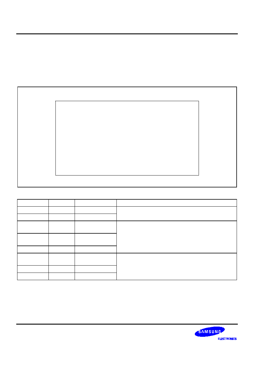
DC/AC Electrical Characteristic
Characteristics
Min
Typ
Max
Unit
Remarks
Supply
Voltage
V
Power
dissipation
mW
Resolution
Bits
Analog
Output
Voltage
V
Operating
Temperature
°
C
Output
Load
Capacitor
pF
Output
Load
Resistor
Integral
Non-Linearity
Error
LSB
Differential
Non-Linearity
Error
LSB
Maximum
Conversion
Rate
MHz
Voltage Output DAC
Characteristics
Min
Typ
Max
Unit
Remarks
Reference Voltage TOP
BOTTOM
V
Analog Output Voltage Range
V
Digital Input Format
Binary Code or 2's Complement Code
Current Output DAC
Characteristics
Min
Typ
Max
Unit
Remarks
Analog
Output
Maximum
Current
mA
Analog
Output
Maximum
Signal
Frequency
MHz
Reference
Voltage
V
External
Resistor
for
Current
Setting (RSET)
Pipeline
Delay
sec
·
Do you want to Power down mode?
·
Do you want to Internal Reference Voltage (BGR)?
·
Which do you want to Serial Input TYPE or parallel Input TYPE?
·
Do you need 3.3V and 5V power supply in your system?
8-BIT 0.5MSPS DAC
AL1213A
12
HISTORY CARD
Version
Date
Modified Items
Comments
Ver 1.0
Jun.'98
Original version published
Ver 2.0
Feb.'00
Core layout Guide update
Ver 2.1
Apr.'02
Phantom Cell information update