AL1214A
12-BIT 160MSPS DAC
1
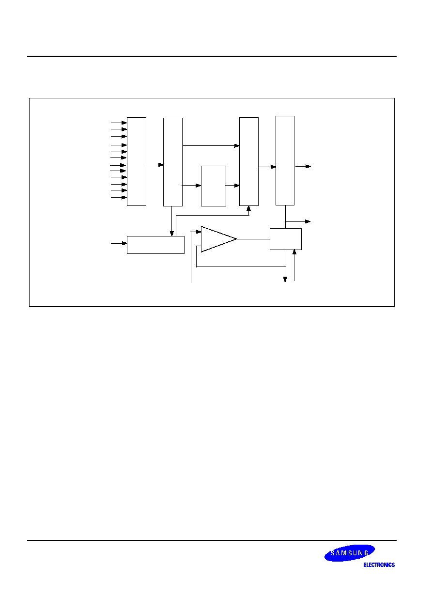
GENERAL DESCRIPTION
The AL1214A is a CMOS 12-bit D/A converter for general applications. Its maximum conversion rate is 160MSPS
and supply voltage is 5V single. An external 3.2V voltage reference (VBIAS) and a single resister (RSET) control
the full-scale output current .
FEATURES
·
160MSPS pipeline operation
·
5V CMOS monolithic construction
·
±
0.3LSB differential linearity (typical)
·
±
1.5LSB internal linearity (typical)
·
External voltage reference
·
12-bit voltage parallel input
TYPICAL APPLICATIONS
·
High Definition Television (HDTV)
·
Hard Disk Drive
·
High Resolution Color Graphics
·
CAE/CAD/CAM
·
ATE (Auto Test Equipment)
AL1214A
12-BIT 160MSPS DAC
5
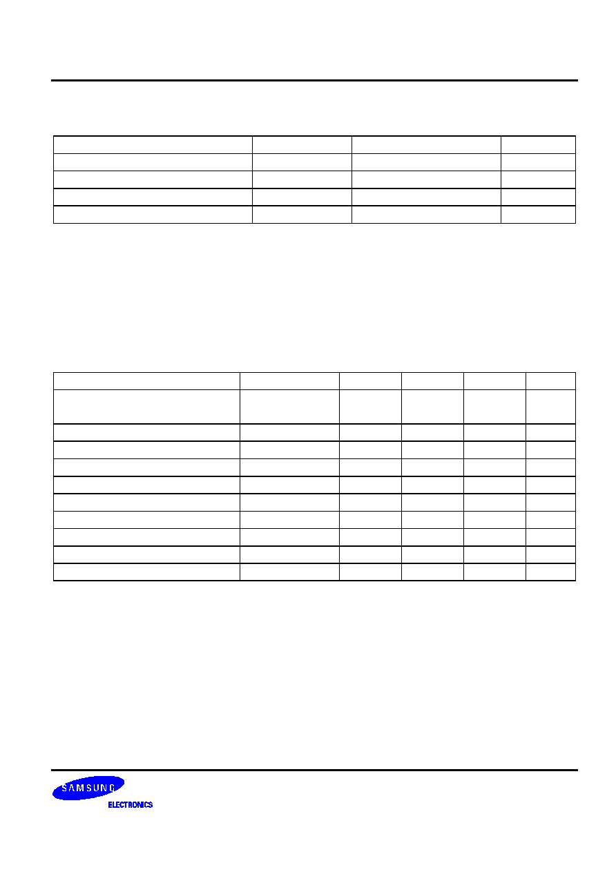
ABSOLUTE MAXIMUM RATINGS
Characteristics
Symbol
Min
Unit
Supply Voltage
VDDD,VDDA
-0.5 ~ +6.5
V
Reference Input Voltage
Vin
VSSD-0.25 to VDDD+0.25
V
Operating Temperature Range
Topr
0 to +70
°
C
Storage Temperature Range
Tstg
-55 to +150
°
C
NOTES:
1.
Absolute maximum rating values applied individually while allother parameters are within specified operating condition.
Function operation under any of these conditions is not implied.
2.
Applied voltage must be current limited to specified range
3.
Absolute maximum ratings are value beyond which the device may be damaged permanently. Normal operation is not
guaranteed.
RECOMMENDED OPERATING CONDITIONS
Characteristics
Symbol
Min
Typ
Max
Unit
Operating Supply Voltage
VDDD-VSSD
VDDA-VSSA
4.75
5.0
5.25
V
Digital Input Voltage High
VIH
4.5
-
-
V
Digital Input Voltage Low
VIL
-
-
0.5
V
Operating Temperature Range
TOPR
0
-
70
°
C
Output Load (effective)
RL
-
160
-
Reference Voltage
VREF
-
3.2
-
V
Clock Cycle Time
Tclk
-
50
-
ns
Clock Pulse Width High
Tpwh
-
25
-
ns
Clock Pulse Width Low
Tpwl
-
25
-
ns
IREF Current
Iref
-
1.4
-
mA
NOTES:
1.
It is strongly recommended that to avoid power latch-up all the supply pins(VDDA,VDDD) be driven from the same
source.
2.
Voltage on any digital pin that goes below VSSD (Digital Ground) by less than 0.3V can induce destructive latch-up