 | –≠–ª–µ–∫—Ç—Ä–æ–Ω–Ω—ã–π –∫–æ–º–ø–æ–Ω–µ–Ω—Ç: al2005h | –°–∫–∞—á–∞—Ç—å:  PDF PDF  ZIP ZIP |
The AL2005H is a Phase-Locked Loop (PLL) frequency synthesizer
constructed in CMOS on single monolithic structure. The PLL Mac-
rofunctions provide frequency multiplication capabilities. The output
frequency Fout is related to the reference input clock frequency Fin
by the following equation:
Fout = ( m*Fin ) / ( p*s)
Where,
Fout is the output clock frequency.
Fin is the reference input clock frequency.
m,p and s are the values for programmable dividers.
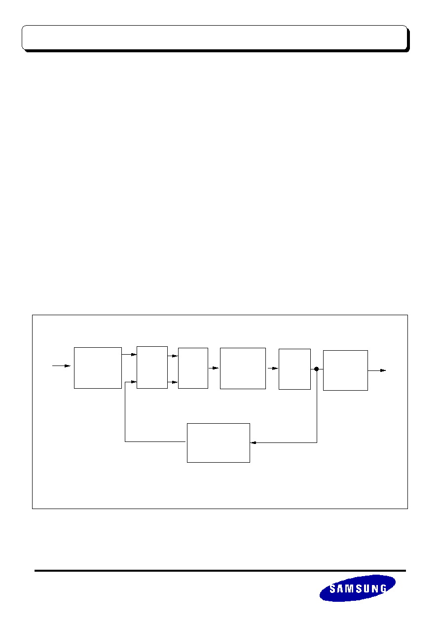
AL2005H consists of a Phase/Frequency Detector(PFD), a Charge
Pump an External Loop Filter, a Voltage Controlled Oscillator(VCO),
a 6bit Pre-divider, an 8bit Main divider and 2bit Post Scaler as
shown in Figure1.
°þ
0.5
ß-
CMOS Process Technology
°þ
5 Volt Single Power Supply
°þ
Output frequency Range: 20~ 170 MHz
°þ
Jitter
°æ
250ps
°þ
Input Duty Ratio 40% to 60%
°þ
Output Duty Ratio 40% to 60%
°þ
Frequency Changed by Programmable Divider
°þ
Power Down Mode
General Description
Features
FUNCTIONAL BLOCK DIAGRAM
Fin
Pre Divider
P
Charge
Pump
PFD
VCO
Main Divider
M
Post Scaler
S
Loop Filter
(External)
Fout
Figure 1. Phase Lockd Loop Block Diagram
20MHz ~ 170MHz FSPLL
AL2005H
SAMSUNG ELECTRONICS Co. LTD
DECEMBER 1998. Ver1.0

SEC ASIC
20MHZ~170MHZ FSPLL
ANALOG
2 / 16
AL2005H
NAME
I/O
TYPE
I/O PAD
PIN DESCRIPTION
VDD
DP
vdd5t
Digital power supply
VSS
DG
vsst
Digital ground
VDDA
AP
vdda
Analog power supply
VSSA
AG
vssa
Analog ground
FIN
DI
pic_bb
PLL clock input
FILTER
AO
poar50_bb
. Pump out is connected to Filter
. A capacitor is connected between the pin
and analog ground
FOUT
DO
custom
driver buffer
20MHz~170MHz clock output
PWRDN
DI
pic_bb
PLL power down.(Enable High)
-If isn't used this pin, tied to VSS.
P[5:0]
DI
pic_bb
The values for 6bit programmable pre-divider.
M[7:0]
DI
pic_bb
The values for 8bit programmable main divider.
S[1:0]
DI
pic_bb
The values for 2bit programmable post scaler.
CORE PIN DESCRIPTION
I/O TYPE ABBR.
°§
AI : Analog Input
°§
DI : Digital Input
°§
AO : Analog Output
°§
DO : Analog Output
°§
AP : Analog Power
°§
AG : Analog Ground
°§
AB : Analog Sub Bias
°§
DP : Digital Power
°§
DG : Digital Ground
°§
DB : Digital Sub Bias
°§
BD : Bidirectional Port
CORE CONFIGURATION
¢∫
°·
¢∫
°·
¢∫
°·
¢∫
°·
FIN
PWRDN
M[0]
M[1]
M[2]
M[3]
M[4]
M[5]
M[6]
M[7]
P[0]
P[1]
P[2]
P[3]
P[4]
P[5]
S[0]
S[1]
FOUT
FILT ER
al2005h
¢∫
°·
¢∫
°·
¢∫
°·
M[7:0]
P[5:0]
S[1:0]

SEC ASIC
20MHZ~170MHZ FSPLL
ANALOG
3 / 16
AL2005H
ABSOLUTE MAXIMUM RATINGS
(Ta=25
°…
)
Characteristics
Symbol
Value
Unit
Applicable pin
DC Supply Voltage
V
DD
V
DDA
-0.5 to +7.0
V
VDD,VDDA,VSS,VSSA
DC Input Voltage
V
I N
Vss-0.3 to Vdd+0.3
V
P<5:0>,M<7:0>
S<1:0>,PWRDN
Storage Temperature
T
STG
-40 to 125
°…
-
NOTES
1. ABSOLUTE MAXIMUM RATING specifies the values beyond which the device may be damaged
permanently. Exposure to ABSOLUTE MAXIMUM RATING conditions for extended periods may affect
reliability. Each condition value is applied with the other values kept within the following operating
conditions and function operation under any of these conditions is not implied.
2. All voltages are measured with respect to VSS unless otherwise specified.
3. 100pF capacitor is discharged through a 1.5
ß⁄
resistor (Human body model)
Recommended Operating Conditions
Characteristics
Symbol
Min
Typ
Max
Unit
Supply Voltage
V
DD
V
DDA
4.75
5
5.25
V
Supply Voltage Difference
V
DD
-V
DDA
-0.1
0
0.1
V
Input Frequency
F
I N
14.318
Mhz
External Loop Filter Capacitance
L
F
-
560
-
pF
Operating Temperature
T
OPR
0
70
°…
NOTES
It is strongly recommended that all the supply pins (VDDA, VDD) be powered from the same source to avoid power latchup
SEC ASIC
20MHZ~170MHZ FSPLL
ANALOG
4 / 16
AL2005H
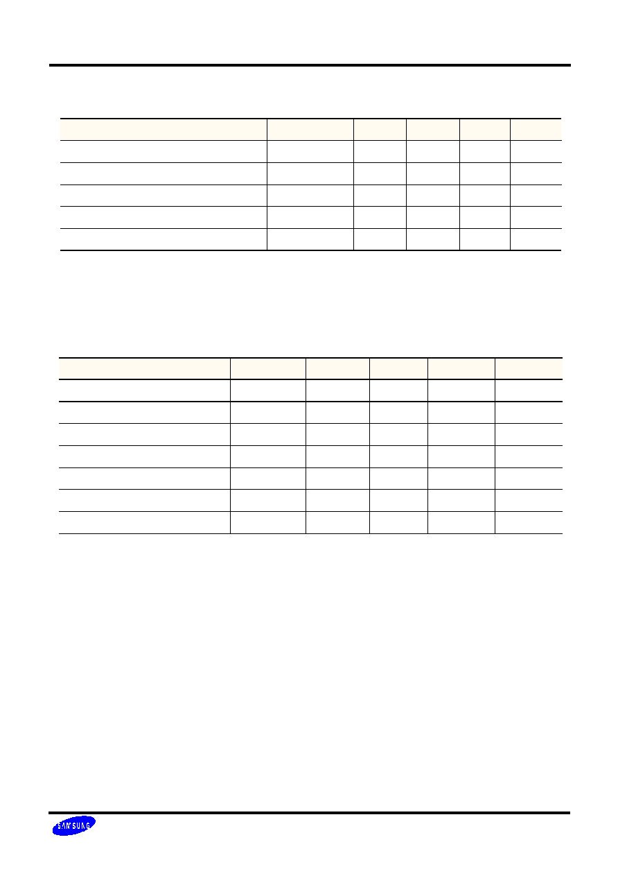
AC ELECTRICAL CHARACTERISTICS
Characteristics
Symbol
Min
Typ
Max
Unit
Input Frequency
F
I N
4
14.318
40
MHz
Input Clock Duty Cycle
T
I D
40
60
%
Output Clock Frequency
F
OUT
20
170
Mhz
Output Clock Duty Cycle
T
OD
40
60
%
Lock-In Time
T
LT
150
us
Jitter
T
J
-250
+250
ps
*Input Glitch Pulse Width
T
I GP
1
ns
DC ELECTRICAL CHARACTERISTICS
Characteristics
Symbol
Min
Typ
Max
Unit
Operating Voltage
V
DD
/V
DDA
4.75
5
5.25
V
Digital Input Voltage High
V
I H
2.0
V
Digital Input Voltage Low
V
I L
0.8
V
Dynamic Current
I
DD
8
mA
Power Down Current
I
PD
80
uA
Note : Avoid to input glitch pulse, if glitch pulse generates to the input, the output frequency will be changed by glitch pulse.

SEC ASIC
20MHZ~170MHZ FSPLL
ANALOG
5 / 16
AL2005H
Functional Description
A PLL is the circuit synchronizing an output signal (generated by a VCO) with a reference
or input signal in frequency as well as in phase.
In this application, it includes the following basic blocks.
. The Voltage-Controlled Oscillator to generate the output frequency
. The divider P to devide the reference frequency by p
. The divider M to devide the VCO output frequency by m
. The divider S to divide the VCO output frequency by s
. The phase&frequency detector detects the phase difference between the reference frequency
and the output frequency (after division) and control the charge pump voltage.
. The loop filter to filter out high frequency components in charge pump voltage and give
smooth and clean control to VCO
The m, p, s values can be programmed by
16bit
digital
data from the external source. So,
the PLL can be locked onto the desired frequency.
Fout = ( m * Fin ) / ( p*s )
Fin = 14.318MHz, m=M+8 , p=P+2, s=2^S
Digital data format:
NOTES
. S1 - S0 : Output Frequency Scaler
. M7 - M0 : VCO Frequency Divider
. P5 - P0 : Reference Frequency Input Divider
Main Divider
Pre Divider
Post Scaler
M7,M6,M5,M4,M3,M2,M1,M0
P5,P4,P3,P2,P1,P0
S0,S1
SEC ASIC
20MHZ~170MHZ FSPLL
ANALOG
6 / 16
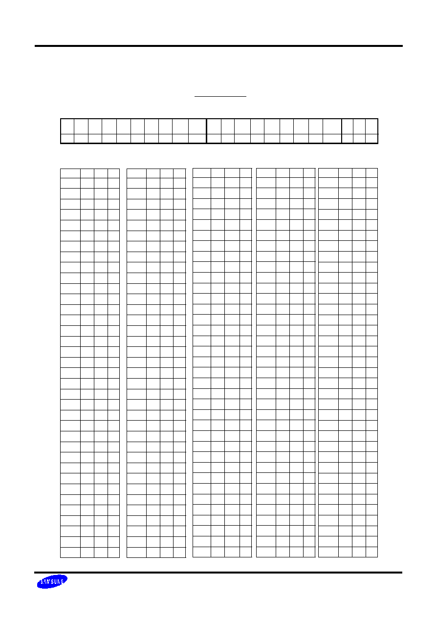
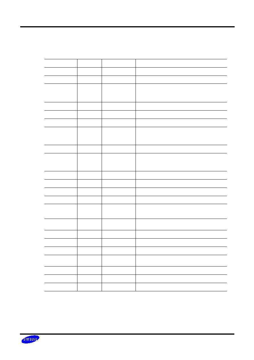
AL2005H
Fout
P
M
S
10
15
87
3
14.318
8
72
3
15
19
168
3
16
15
68
2
17
10
49
2
18
27
138
2
19
11
61
2
20
15
87
2
21
13
80
2
22
12
78
2
23
24
159
2
24
25
173
2
25.175
23
168
2
25.5
14
106
2
26
17
130
2
27
22
173
2
28.322
21
174
2
29
8
73
2
30
19
168
2
30.25
18
161
2
31
7
70
2
31.5
8
80
2
32
15
144
2
32.514
17
79
1
33
21
98
1
34
10
49
1
35
36
80
1
35.5
22
111
1
36
18
93
1
37
10
54
1
37.5
15
81
1
38
11
61
1
39
27
150
1
39.5
27
152
1
40
15
87
1
41
9
55
1
Fout
P
M
S
41.6
19
144
1
42
13
80
1
43
8
52
1
44
25
158
1
44.3
14
91
1
44.74
10
67
1
44.9
9
61
1
45.5
12
81
1
46
24
159
1
47
21
143
1
48
15
106
1
49
11
81
1
49.2
22
157
1
49.5
10
75
1
50
8
62
1
50.35
23
168
1
51
22
163
1
52
17
130
1
53
8
66
1
54
9
75
1
55
20
161
1
56
15
125
1
56.644
21
174
1
57
22
183
1
58
8
73
1
59
19
165
1
60
19
168
1
61
21
188
1
62
13
122
1
62.5
9
88
1
63
8
80
1
64
15
144
1
65
11
110
1
66
12
121
1
66.6
12
123
1
68
12
125
1
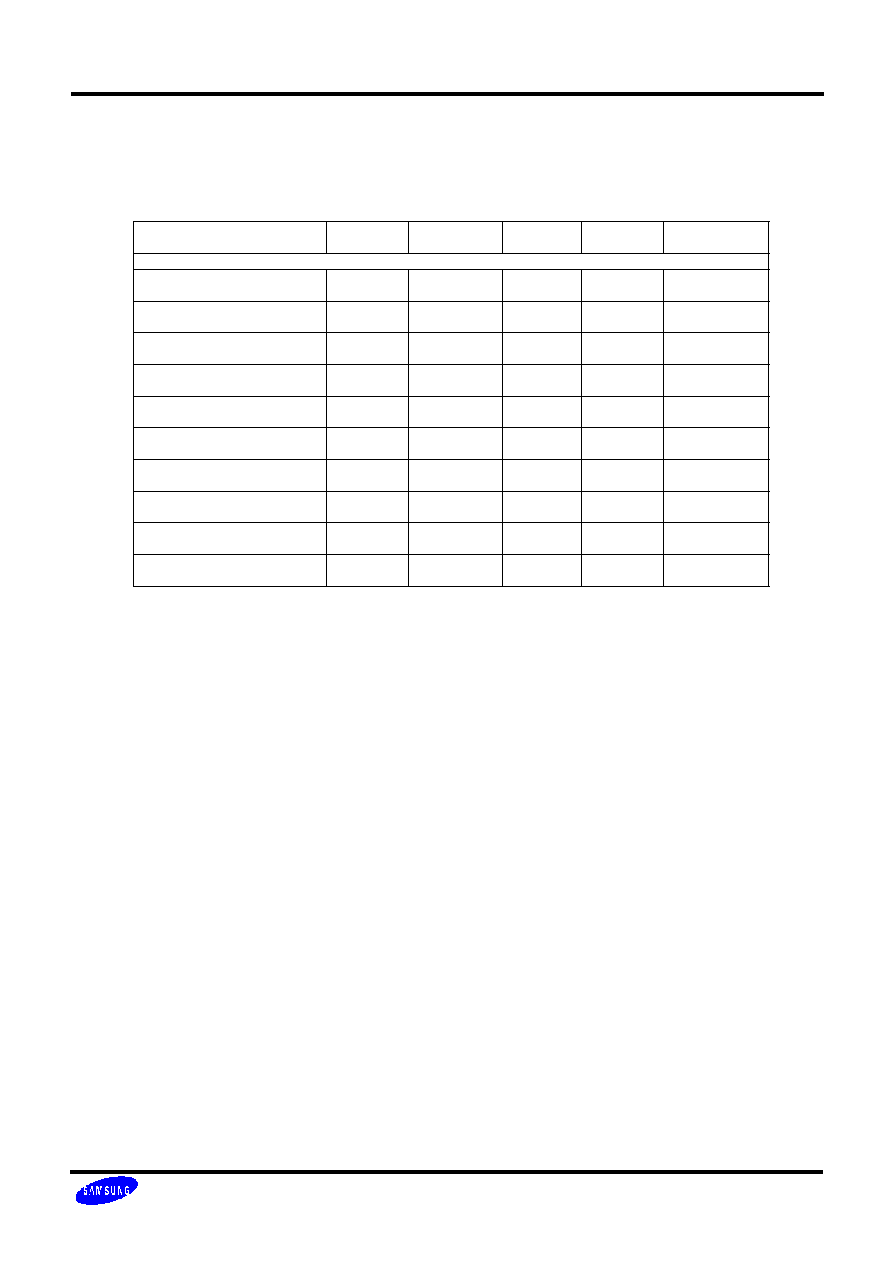
Fout
P
M
S
69
9
98
1
70
16
80
0
71
22
111
0
72
18
93
0
73
18
94
0
74
10
54
0
75
15
81
0
76
11
61
0
77
14
78
0
77.25
21
116
0
78
18
101
0
79
27
152
0
80
15
87
0
81
30
173
0
82
9
55
0
83.04
13
79
0
84
13
80
0
85
14
87
0
86
8
52
0
87
11
71
0
88
25
158
0
89
12
79
0
89.8
9
61
0
91
12
81
0
92
24
159
0
93
8
57
0
93.4
17
116
0
94.5
8
58
0
95
9
65
0
95.5
7
52
0
96
15
106
0
97
20
141
0
98
11
181
0
99
21
151
0
99.7
25
180
0
100.
8
62
0
Fout
P
M
S
100.76
25
182
0
101
17
126
0
102
22
163
0
103
19
143
0
104
17
140
0
105
10
80
0
106
8
66
0
107
17
134
0
108
22
173
0
109
16
129
0
110
20
161
0
111
14
116
0
112
15
125
0
113
17
142
0
114
22
183
0
115
22
185
0
116
8
73
0
117
21
180
0
118
23
198
0
119
14
125
0
120
19
168
0
121
18
161
0
122
21
188
0
123
20
181
0
124
7
70
0
125
9
88
0
126
8
80
0
127
13
125
0
128
14
135
0
129
8
82
0
130
11
110
0
131
18
175
0
132
7
75
0
133
19
187
0
134
12
123
0
135
12
124
0
Fout
P
M
S
136
0
11
0
137
5
59
0
138
23
233
0
139
22
225
0
140
7
80
0
141
11
120
0
142
10
111
0
143.18
7
82
0
144
15
163
0
145
6
73
0
146
3
43
0
147
13
146
0
148
1
23
0
149
20
221
0
150
19
212
0
151
9
108
0
152
11
130
0
153
17
195
0
154
2
35
0
155
21
241
0
156
17
199
0
157
22
255
0
158.12
21
246
0
159
17
203
0
160
21
249
0
161
2
37
0
162
17
207
0
163
11
140
0
164
9
118
0
165
19
234
0
166
20
247
0
167
7
97
0
168
13
168
0
169
13
169
0
170
6
127
0
OUTPUT FREQUENCY EQUATION & TABLE
Table 2. Sample Frequency Coefficient(Reference Input Frequency=14.318MHz)
F
OUT
=
(m+8)
(p+2) x 2
s
x F
IN
M7
M6
M5
M4
M3
M2
M1
M0
m
M
(m+8)
P6
P5
P4
P3
P2
P1
P0
p
P
(p+2)
S1
S0
2
S
0
1
0
1
0
1
0
1
85
93
0
1
0
1
0
0
1
41
43
0
0
1
Table 1. Example of Divider Ratio
Frequency Equation:

SEC ASIC
20MHZ~170MHZ FSPLL
ANALOG
7 / 16
AL2005H
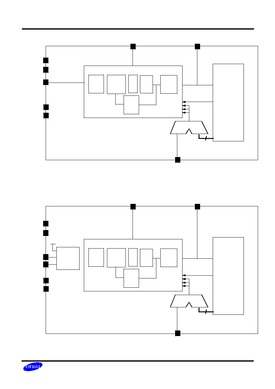
CORE EVALUATION GUIDE
NOTES
: 10uF ELECTROLYTIC CAPACITOR
UNLESS OTHERWISE SPECIFIED
: 103 CERAMIC CAPACITOR
UNLESS OTHERWISE SPECIFIED
¢∫
°·
¢∫
°·
FOUT
FILTER
AL2005H
#1.16bit Register Block
PWRDN
P<5:0>
S<1:0>
560pF
M<7:0>
¢∫
°·
FIN
External
Clock
Source
VDD
VSS
VDDA VSSA
5V Digital Power
5V Analog Power
GND
GND
VSSA
Select Pin
Test Pins of N Sample bits
(used to primary pad cells)
Internal Divider Signal Line
#2
M
U
X
For the embedded PLL, we must consider the test circuits for the embedded PLL core in
multiple applications. Hence, the following requirements should be satisfied.
- The FILTER and FOUT pins must be provided for test.
- For PLL test (Below 2 examples),
It is needed to control the dividers - M<7:0>,P<5:0> and S<1:0> -that generate multiple clocks.
#1. Registers can be used for easy control of divider values.
#2. N sample bits of 16-bit divider pins can be bypassed for test using MUX.

SEC ASIC
20MHZ~170MHZ FSPLL
ANALOG
8 / 16
AL2005H
- The digital power(VDD,VSS) and the analog power(VDA,VSSA) must be dedicated to PLL seperately.
If the dedicated VDD and VSS is not allowed, the pins of the smallest power consuming block are
shared with the PLL.
- The POAR50_BB pad is used as a FILTER pad that contains ESD production diodes and 50
ߟ
resistor
without buffers.
- The FOUT and FILTER pins must be placed away from the internal signals in order to avoid overlapping
signal lines.
- The blocks having a large digital switching current must be located away from the PLL core.
- The PLL core must be shielded by guardring.
- For the FOUT pad, you can use a custom drive buffer or POT4_BB buffer considering the drive current.
CORE LAYOUT GUIDE
Oscillator Cell USERS GUIDE (PLL Typical Input 14.318MHz)
- There is crystal driver cell options for the AL2005H PLL core. PSOSCM2 is 10MHz-40MHz programmable
Input Oscillator Cell with Enable.(Refer to Figure 2)
If a wide range of crystal component is used instead of a 14.318MHz, it is recommended to use STD85's
10MHz-40MHz programmable PSOSCM2 with a positive enable pin like Figure2. A crystal component is
located between the PADA pin and the PADY pin.
- When implementing an embedded PLL block, the following pins must are provided for testing the PLL
locking function:
* Normal Case : FIN,FILTER,FOUT,VDDA,VSSA,VDD and VSS.
* Used Crystal Pad Cells(Used PSOSCM2) : PADA,PADY,FILTER,FOUT,VDDA,VSSA,VDD and VSS
- A special XTAL pad(PSOSCM2) for PLL is supported, Order chapter 4 for details.(STD85 Data Book)
- The XTAL must be located between PADA and PADY Enable pin(E) must be HIGH in normal operation.
- The Operating Frequency of PSOSCM2 is 10MHz ~ 40MHz.
- PI pin must be connected to VDD and PO pin floated.
Figure 2. XTAL PAD Symbol (PSOSCM2)
E
PADA
PADY
YN
PI
PO
SEC ASIC
20MHZ~170MHZ FSPLL
ANALOG
9 / 16
AL2005H
FOUT
P[5:0]
M[7:0]
S[1:0]
PWRDN
VDDA
VSSA
VDD
VSS
Glue Logics
MUX
*Optional Test Pins
*Divider Bus
Divider
P
PFD
&CP
LF
VCO
Scaler
S
Divider
M
FILTER
FIN
FOUT
P[5:0]
M[7:0]
S[1:0]
PWRDN
XTALIN
XTALOUT
PSOSCM2
VDDA
VSSA
VDD
VSS
Glue Logics
E(VDD Tie)
PADA
PADY
MUX
*Optional Test Pins
*Divider Bus
Divider
P
PFD
&CP
LF
VCO
Scaler
S
Divider
M
FILTER
Figure 4. The example of PLL block with SEC's XTAL-OSC(PSOSCM2)
Figure3. The example of PLL block without crystal component (Normal Case)

SEC ASIC
20MHZ~170MHZ FSPLL
ANALOG
10 / 16
AL2005H
PACKAGE CONFIGURATION (48QFP)
2
1
4
3
6
5
8
7
10
9
12
11
35
36
33
34
31
32
29
30
27
28
25
26
13
14
15
16
17
18
19
20
21
23
24
48
47
46
45
44
43
42
41
40
39
38
37
22
N
C
V
D
D
V
S
S
P
W
R
D
N
P
0
P
1
P
2
P
3
P
4
P
5
N
C
N
C
NC
VDDA
VSSA
OSCDIS
FIN/XTALIN
XTALOUT
VSSAP
VDDAP
VFOUT
FOUT
FILTER
NC
N
C
V
0
V
1
V
2
V
3
V
4
V
5
N
C
V
S
S
P
A
C
O
U
T
V
D
D
P
A
C
I
N
NC
S0
S1
M0
M1
M2
M3
M4
M5
M6
M7
RO
AL2005H
C
10uF
103
C
C
C
C
L
H
L
H
L
H
L
H
L
H
L
H
L
H
L
H
L
H
L
H
L
H
L
H
L
H
L
H
L
H
L
H
L
H
L
H
L
H
L
H
L
H
L
H
L
H
NOTES
1.V0~V5,VFOUT,RO,ACIN and ACOUT pins are internal dummy block test pins.
So, V0~V5 and ACIN tied to VDD or VSS, and RO,ACOUT pins have to float
the output pin.
560pF
5V Analog PAD Power
5V Analog Power
14.318MHZ
L
H
5V Digital Power
6bit
Pre
Divider
Input
2bit Post Scaler
8bit Main Divider
Dummy Test Block Control pins
5V Digital PAD Power
SEC ASIC
20MHZ~170MHZ FSPLL
ANALOG
11 / 16
AL2005H
NAME
PIN NO
I/O TYPE
PIN DESCRIPTION
VDD
2
DP
PLL Core Digital power supply
VSS
3
DG
PLL Core Digital ground
PWRDN
4
DI
FSPLL clock power down
-PWRDN is High, PLL do not operating under
this condition.
-If isn't used this pin, tied to VSS.
P0~P5
5~10
DI
6Bit Pre-Divider Input
VDDA
14
AP
PLL Core Analog power supply
VSSA
15
AG
PLL Core Analog ground
OSCDIS
16
DI
XTAL-OSC enable/disable control pin.
-OSCDIS is HIGH, PLL don't operating under
this condition.
-If isn't used this pin, tied to VSS
FIN/XTALIN
17
AI
External clock source input or crystal input
XTALOUT
18
AO
Crystal output
-If a crystal is used, it is connected across
the I/O pins XTALIN and XTALOUT.
If isn't used it has to float the output.
VSSAP
19
PG
Analog PAD ground
VDDAP
20
PP
Analog PAD supply power
VFOUT
21
DO
Fout Divided by 1/[3~65] output test pin.
FOUT
22
DO
20MHZ~170MHz clock output
FILTER
23
AO
Pump out is connected to the FILTER.
A 560pF Capcitor is connected between the
pin and analog pin
V0~V5
26~31
DI
VFOUT divide control pins.
-End users used not this pins, tied to VDD or VSS
VSSP
33
PG
Digital PAD ground
ACOUT
34
DO
Internal Dummy test block output
VDDP
35
PP
Digital PAD supply power
ACIN
36
DI
Internal Dummy test block input
Do not float this pin. must be tie to VDD or VSS
S0~S1
38~39
DI
2Bit Post scaler input
M0~M7
40~47
DI
8bit main divider input
RO
48
DO
Internal Dummy test block output
NOTE: NC means no connection.
PACKAGE PIN DESCRIPTION (48QFP)

SEC ASIC
20MHZ~170MHZ FSPLL
ANALOG
12 / 16
AL2005H
PACKAGE CONFIGURATION (100QFP)
1. nc
100. nc
2. nc
3. nc
4. nc
5. nc
6. nc
7. nc
8. nc
9. nc
10. vdd
11. vss
12. pwrdn
13. p0
14. p1
15. p2
16. p3
17. p4
18. p5
19. nc
20. index1
21. nc
22. nc
23. nc
24. nc
25. nc
26. nc
27. nc
28. nc
29. nc
30. nc
99. nc
98. nc
97. nc
96. ro
95. m7
94. m6
93. m5
92. m4
91. m3
90. m2
89. m1
88. m0
87. s1
86. s0
85. nc
84. nc
83. nc
82. nc
81. nc
31. nc
32. nc
33. nc
34. nc
35. index2
36. vdda
37. vssa
38. oscdis
39. xtalin
40. xtalout
41. vssap
42. vddap
43. vfout
44. fout
45. filter
46. nc
47. nc
48. nc
49. nc
50. nc
80. nc
79. nc
78. nc
77. nc
76. nc
75. nc
74. nc
73. nc
72. nc
71. acin
70. vddp
69. aout
68. vssp
67. nc
65. v4
64. v3
63. v2
62. v1
61. v0
60. nc
59. nc
58. nc
57. nc
56. nc
55. nc
54. nc
53. nc
52. nc
51. nc
66. v5
ALC005X
100QFP
c
103
10uF
c
1
0
1
0
1
0
1
0
1
0
1
0
1
0
1
0
1
0
1
0
1
0
1
0
1
0
1
0
1
0
1
0
1
0
1
0
1
0
1
0
1
0
1
0
1
0
c
c
1
0
c
560pF
14.318MHz
Analog Power
Analog PAD Power
Digital Power
6Bit Pre Divider
Test Block Control
Didital PAD Power
8Bit Main Divider 2Bit Post Scaler
TESTBANK 85

SEC ASIC
20MHZ~170MHZ FSPLL
ANALOG
13 / 16
AL2005H
NOTES : NC means no connection.
PACKAGE PIN DESCRIPTION (100QFP)
NAME
PIN NO
I/O TYPE
PIN DESCRIPTION
VDD
10
DP
PLL Core Digital power supply
VSS
11
DG
PLL Core Digital ground
PWRDN
12
DI
FSPLL clock power down
-PWRDN is High, PLL do not operating under
this condition.
-If isn't used this pin, tied to VSS.
P0~P5
13~18
DI
6Bit Pre-divider input
VDDA
36
AP
PLL Core Analog power supply
VSSA
37
AG
PLL Core Analog ground
OSCDIS
38
DI
XTAL-OSC enable/disable control pin.
-OSCDIS is HIGH, PLL don't operating under
this condition.
-If isn't used this pin, tied to VSS
XTALIN/FIN
39
AI
External Clock Source or Crystal input
XTALOUT
40
AO
Crystal output
-If a crystal is used, it is connected across
the I/O pins XTALIN and XTALOUT.
If isn't used it has to float the output.
VSSAP
41
PG
Analog PAD ground
VDDAP
42
PP
Analog PAD supply power
VFOUT
43
DO
Fout Divided by 1/[3~65] output test pin.
FOUT
44
DO
20MHZ~170MHz clock output
FILTER
45
AO
Pump out is connected to the FILTER.
A 560pF Capcitor is connected between the
pin and analog pin
V0~V5
62~66
DI
VFOUT divide control pins.
-End users used not this pins, tied to VDD or VSS
VSSP
68
PG
Digital PAD ground
ACOUT
69
DO
Internal Dummy test block output
VDDP
70
PP
Digital PAD supply power
ACIN
71
DI
Internal Dummy test block input
Do not float this pin. must be tie to VDD or VSS
S0~S1
86~87
DI
2Bit Post scaler input
M0~M7
88~95
DI
8Bit Main divider input
RO
96
DO
Internal Dummy test block output

SEC ASIC
20MHZ~170MHZ FSPLL
ANALOG
14 / 16
AL2005H
PLL Introduction
De-Skew Function
In semiconductor manufacturing, smaller device geometry facilitate greater on-chip density and higher chip
performance. System performance is compromised, however, by clock skew which occures when the clock
on a chip is not synchronized to the system clock. The degree of clock skew varies from chip to chip
because of variations in process, temprature, power supply, interconnects, and routing. The PLL trackes
the system clock and compares it with the on-chip clock, then adjusts the latter until it matches the former
in frequency and phase.
Frequency Synthesis Function
Frequency synthesis uses the system clock as a base frequency to generate higher/lower frequency clocks
for internal logic. For high speed applications in high-end designs, transmission line effects cause problems
because of parastics and impedance mismatch among various on-board components. These problems can be
eliminated by moving the high frequency to the chip level. On-chip clocks that are faster than the external
system clock can be synthesized by inserting a divider in the feedback path. The divider is placed after voltage
controlled oscillator, as illustrated in Figure1. The signal is running at M times the system clock frequency, so
the PLL matches the divider signal output to the system clock. This configuation reduces the problem of
interfacing to the system clock on the board, and it reduces the noise generated by the system clock oscillator
and driver for all the components in the system
PLL Components
Figure5 is block diagram of the components of a PLL: phase frequency detector, charge pump, voltage controlled
oscillator, and loop filter. In SEC technology, the loop filter is implemented as external components close to chip.
Phase detector : The phase dectector monitors the phase difference between the Fin and Fout, and generates a
control signal when it detects difference between the two. If the Fin frequency is higher than the Fout frequency,
its falling edge occures before(lead) the falling edge of the Fout output. When this occures the phase detector
signals the VCO to increase the frequency of the on-chip clock. If the falling edge of the Fin occures after(lag)
the falling edge of the Fout output, the detector signals the VCO to decrease on-chip clock frequency. If the
frequencies of the Fin and Fout are the same, the detector does not generate a control signal, so the
frequencies remain the same.
Charge Pump : The charge pump converts the phase detector control signal to a charge in voltage across the
external filter that drives the VCO. As the Voltage Controlled Oscillator decreases, or increases, If the voltage
remains constant, the frequency of the oscillator remains constant.
Loop Filter
: The control signal that the phase detector generates for the charge pump may generate large
excursions (ripples) each time the VCO output is compared to the system clock. To avoid overloading the VCO,
a low pass filter samples and filters the high-frequency components out of the control signal. the filter is typically
a single-pole RC filter consisting of a resistor and capacitor.
Voltage Controlled Oscillator(VCO) : The output voltage from the loop filter drives the VCO, causing its
oscillation frequency to increas or decrease as a function of variations in voltage. When the VCO output
matches the system clock in frequency and phase, the pahse detector stops sending a control signal to the
charge pump, which in turn stabilizes the input voltage to the loop filter. The frequency then remains constant,
and the PLL remains locked onto the system clock.

SEC ASIC
20MHZ~170MHZ FSPLL
ANALOG
15 / 16
AL2005H
Design Considerations
The following design consideratios apply:
* Phase tolerance and jitter are independent of the PLL frequency.
* Jitter is affected by the noise frequency in the power(VDD/VSS,VDDA/VSSA) .It increases when the
noise level increases.
* A CMOS-level input reference clock is recommend for signal compatibility with the PLL circuit. Other
levels such as TTL may degrade the tolerances.
* The use of two, or more PLLs requires special design considerations. Please contact SEC's application
engineer for more information.
* The following apply to the noise level, which can be minimized by using good analog power and
ground isolation techniques in the system:
- Use wide PCB traces for POWER(VDD/VSS, VDDA/VSSA) connections to the PLL core Seperate
the traces from the chip's VDD/VSS,VDDA/VSSA supplies.
- Use proper VDD/VSS,VDDA/VSSA de-coupling.
- Use good power and ground sources on the board.
* The PLL core should be placed as close as possible to the dedicated loop filter and analog Power
and ground pins.
* It is inadvisable to locate noise-generating signals, such as data buses and high-current outputs, near
the PLL I/O cells.
* Other related I/O signals should be placed near the PLL I/O but do not have any pre-defined
placement restriction
Fin
Charge
Pump
PFD
VCO
Loop Filter
(External)
Fout
Figure 5. Main Components of PLL
SEC ASIC
20MHZ~170MHZ FSPLL
ANALOG
16 / 16
AL2005H
We appreciate your interest in our products. If you have further questions, please specify in
the attached form. Thank you very much.
Parameter
Min
Typ
Max
Unit
Remarks
Supply Voltage
Output frequency range
Input frequency range
Cycle to Cycle Jitter
Lock up time
Dynamic current
Stand by current
Output clock duty ratio
Long term jitter
Output slew rate
- Do you need XTAL driver buffer in PLL Core?
If you need it, what's the crystal frequency range? If not, What's the input frequency range?
- Do you need the lock detector?
- Do you need the I/O cell of SEC?
- Do you need the external pin for PLL test?
- What's the main frequency & frequency range?
- How many FSPLLs do you use in your system?
- What's output loading?
- Could you external/internal pin configurations as required?
Specially requested function list :
PLL Specification