 | –≠–ª–µ–∫—Ç—Ä–æ–Ω–Ω—ã–π –∫–æ–º–ø–æ–Ω–µ–Ω—Ç: BW0404X | –°–∫–∞—á–∞—Ç—å:  PDF PDF  ZIP ZIP |

BW0404X
0.5
µ
µ
M SIGMA-DELTA ADC
1
GENERAL DESCRIPTION
Samsung's BW0404X is high resolution ADC that employs the Sigma-Delta modulation technique. With a
resolution of 14-bit and oversampling X128FS, BW0404X is suitable for speech and telephony applications,
multimedia and digital systems.
TYPICAL APPLICATIONS
∑
Speech Processing (Recognition, Synthesis, Compression etc.)
∑
Telephony
∑
Modem
FEATURES
∑
14-Bit Sigma-Delta A/D converter
∑
2 Channel Analog MUX
∑
Sigma-Delta ADC.
128X Oversampling
2nd Order Sigma-Delta modulator
On-chip Decimation Filter
80dB Signal to Noise Ratio.
∑
Single-ended Analog Input
∑
Serial and Parallel Digital Output
∑
Sampling Rate of 28kHz
∑
Single +5V Power Supply
0.5
µ
µ
M SIGMA-DELTA ADC
BW0404X
2
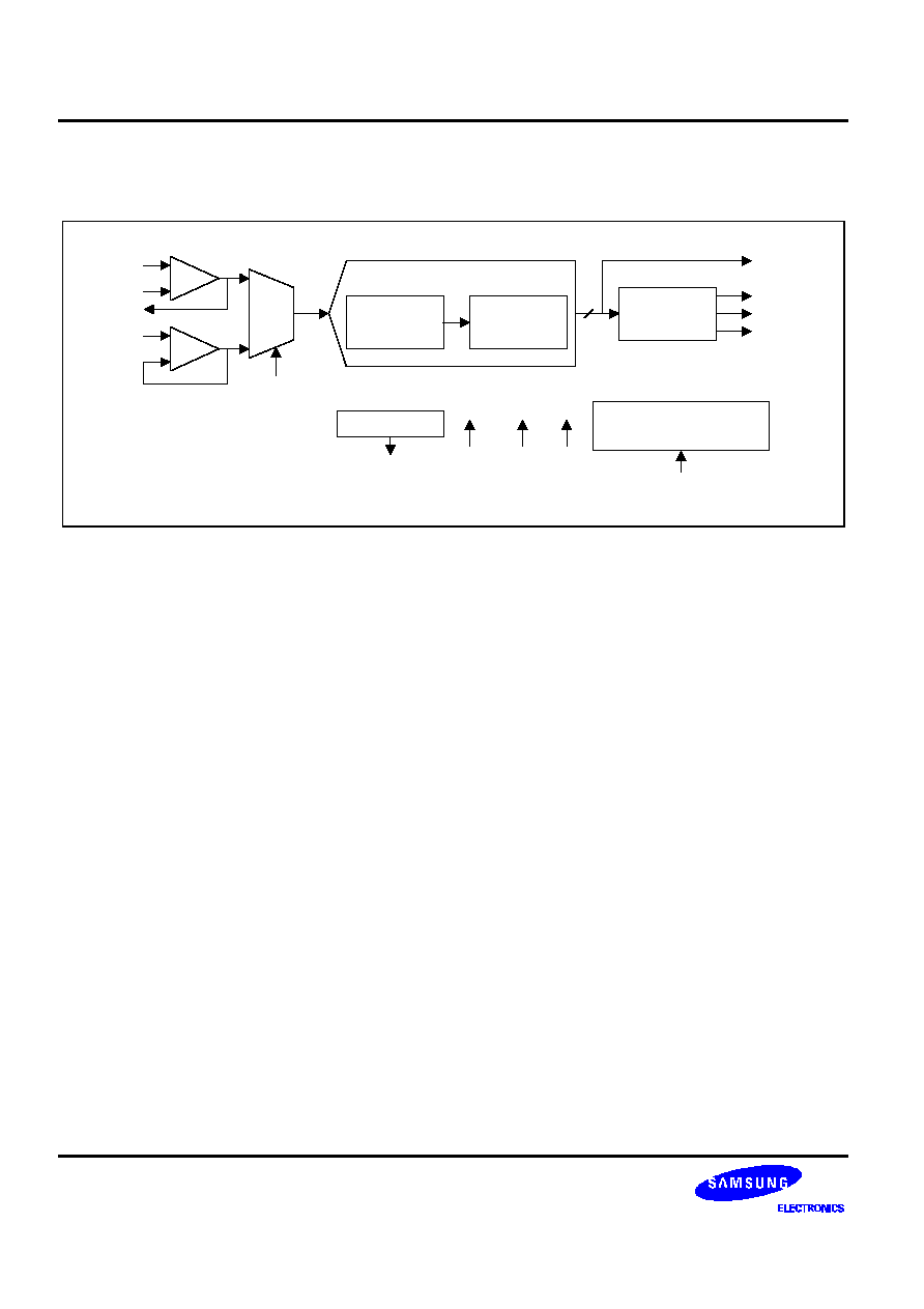
FUNCTIONAL BLOCK DIAGRAM
INSE
INP
14
SDOUT
OPS
PWDN
BCK
FS
MCLK
RSEL
VREF
Sigma-Delta A/D CONVERTER
PDOUT
RST
INN
OUT
AMP
AMP
MUX
Sigma-Delta
Modulator
Decimation
Filter
SERIAL
I/F
REFERENCE
CLOCKGENERATOR
BIST
Ver 1.0 (April 1999)
This data sheet is a preliminary version. No responsibility is assumed by SEC for its use nor for any
infringements of patents or other rights of third parties that may result from its use. The content of this data sheet
is subject to change without any notice.

BW0404X
0.5
µ
µ
M SIGMA-DELTA ADC
3
CORE PIN DESCRIPTION
Name
I/O
Type
I/O
Pad
Pin
Description
Power
VDDA3
AP
vdda
Analog supply power
VSSA3
AG
vssa
Analog ground
VDDA2
AP
vdda
Analog supply power
VSSA2
AG
vssa
Analog ground
VBBA
AG
vbba
Analog ground for substrate bias
VDDA1
DP
vdd5t
Digital supply
VSSA1
DG
vsst
Digital ground
Analog Signals
INSE
AI
pia_bb
Analog input
INP
AI
pia_bb
Analog input (Differential)
INN
AI
pia_bb
Analog input (Differential)
OUT
AO
poa_bb
Analog output (Differential)
VREF
AO
poa_bb
Bypass capacitor pin for reference signal
I/O TYPE ABBR.
∑
AI : Analog Input
∑
DI : Digital Input
∑
AO : Analog Output
∑
DO : Digital Output
∑
AB : Analog Bidirectional
∑
DB : Digital Bidirectional
∑
AP : Analog Power
∑
AG : Analog Ground
∑
DP : Digital Power
∑
DG : Digital Ground
0.5
µ
µ
M SIGMA-DELTA ADC
BW0404X
4
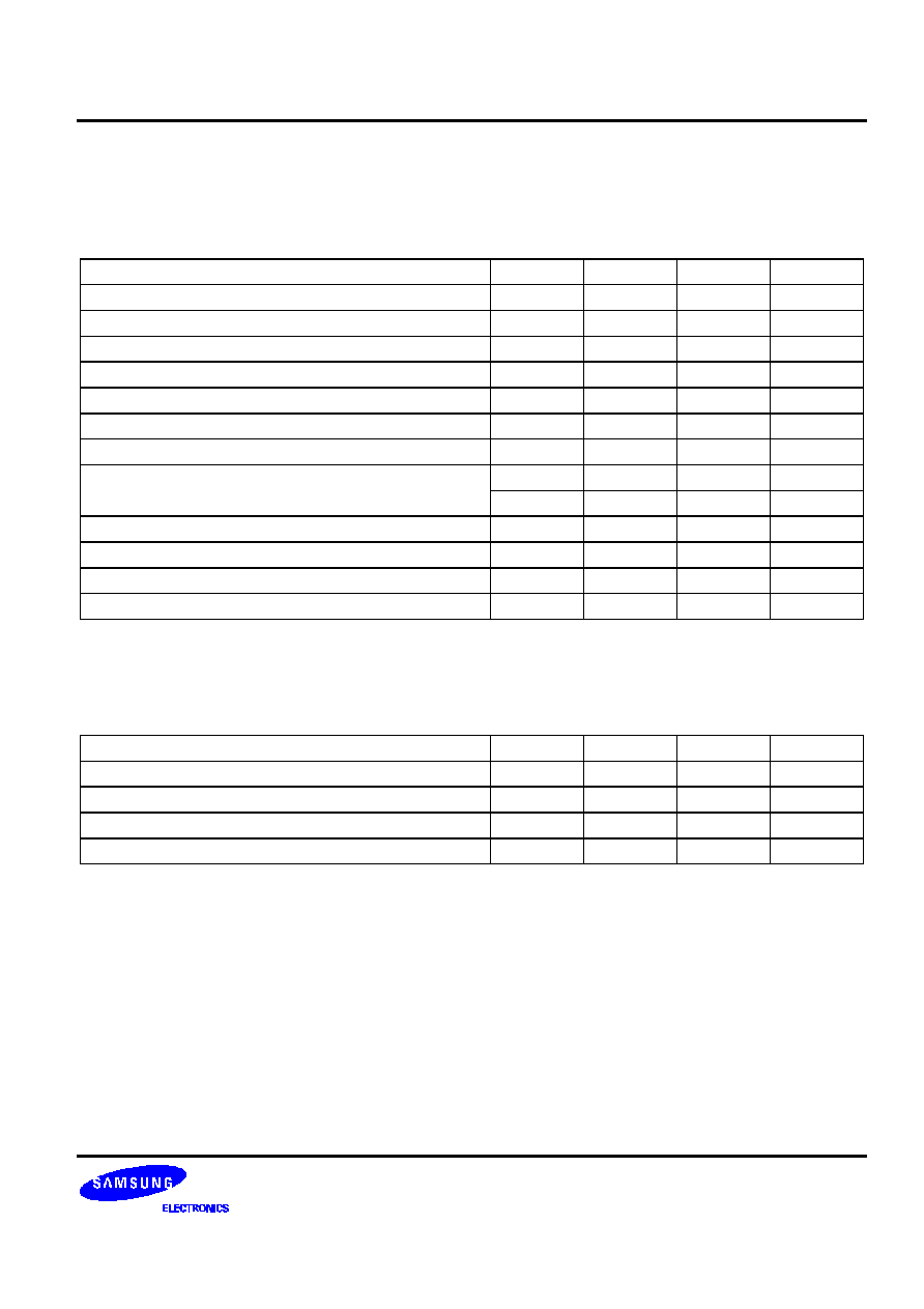
CORE CONFIGURATION
OPS
BCK
BW0404X
USED POWERS
VDDA1, VSSA1, VDDA2, VSSA2,
VDDA3, VSSA3, VBBA
SDOUT
FS
PDOUT{13:0]
INSE
INP
INN
PWDN
MCLK
RSEL
RST
OUT
VREF
ABSOLUTE MAXIMUM RATINGS
Characteristics
Symbol
Value
Units
Supply Voltage
VDD
5
V
Digital Input Voltage
CLK
VSS to VDD
V
Digital Output Voltage
Voh,Vol
VSS to VDD
V
Storage Temperature Range
Tstg
-40 to 125
∞
C
Operating Temperature Range
Topr
0 to 70
∞
C
RECOMMENDED OPERATING CONDITIONS
Characteristics
Symbol
Min.
Typ.
Max.
Units
Supply Voltage
VDDA1-VSSA1
VDDA2-VSSA2
VDDA3-VSSA3
VDD-VSS
4.75
5
5.25
V
Analog Input Voltage range
-
2.818
-
Vp-p
Operating Temp.
Topr
0
-
70
∞
C
BW0404X
0.5
µ
µ
M SIGMA-DELTA ADC
5
ELECTRICAL CHARACTERISTICS
(Measurement Bandwidth is 20Hz ~ 10kHz, Full scale input sine wave 1kHz, Fs = 28kHz, VDDA1, VDDA2,
VDDA3 = 5V, Ta = 25
∞
C, MCLK = 3.584MHz,
ADC
input=2.818Vp-p, Unless otherwise specified)
Characteristics
Min.
Typ.
Max.
Units
Resolution
-
14
-
Bits
Sampling rate
-
28
-
kHz
S/N (EIAJ)
-
85
-
dB
THD
-
72
-
dB
S/(N+D)
-
70
-
dB
Dynamic Range (-60dB Input)
-
72
-
dB
*Offset Error
-
10
-
mV
Analog Input Voltage Range
(INSE)
-
2.1739
-
Vp-p
(INP)
-
2.828
-
Vp-p
*Analog Input Impedance
10
-
-
kW
Power Dissipation
-
20
-
mW
Power Down Current
-
0.05
-
mW
*Power Supply Rejection Ratio
-
TBD
-
dB
CLOCK CHARACTERISTICS
(MCLK = 3.584MHz)
Characteristics
Min.
Typ.
Max.
Units
BCK Frequency(16Fs clock)
-
448
-
KHz
FS Frequency(Fs clock)
-
28
-
KHz
Duty Cycle(MCLK)
40
50
60
%
Tdelay
-
-
10
ns

0.5
µ
µ
M SIGMA-DELTA ADC
BW0404X
6
SERIAL INTERFACE DATA FORMAT
The BW0404X provides 14-bit resolution functions. The digital output of this is through the serial output ports.
The interface block consists of a bit clock(BCK), a frame sync output clock(FS), a serial data output(SDOUT), a
parallel data output(PDOUT). In reset or Power down mode, the digital output goes to zeros. There is digital
interface format. for BW0404X.
BCK
Tdelay
SDOUT
* Guaranteed ; Not tested
FS
(Fs clock)
BCK
(X16Fs)
Parallel 14-bit output
SDOUT
1 Frame
LSB
MSB
PDOUT
13
12
11
10
0
x
x
13
12
11
10
1
x
x
BW0404X Serial Interface Timing Diagram
If you want to test embedded core, it is recommended to add the monitoring pins(SDOUT, BCK, FS) and mux for
data path.
INPUT SOURCE SELECT CONTROL
OPS is to select the one input source between two inputs.
OPS
Input
Source
0
Analog
Differential
Input
(INP.INN)
Select
1
Analog
Single
Input
(INSE)
Select

BW0404X
0.5
µ
µ
M SIGMA-DELTA ADC
7
REFERENCE VOLTAGE SELECT CONTROL
RSEL is to select the one reference voltage between internal and external.
RSEL
Reference
Voltage
0
Internal
Reference
Voltage
Select
1
External
Reference
Voltage
Select
EMBEDDED CORE EVALUATION EXAMPLE
DSP Block
BW0404X
SDOUT
OPS
BCK
FS
VREF
INSE
INN
SDOUT
OPS
RSEL
BCK
FS
On-Chip
1uF
RSEL
PDOUT
330K
INSE
100K
56pF
INN
1uF
INP
INP
OUT
PWDN
PWDN
MCLK
MCLK
PDOUT
External PAD
; For BW0404X Test
1uF
RST
RST
68K
56pF
220K
437K
437K
1uF
100K
56pF
0.5
µ
µ
M SIGMA-DELTA ADC
BW0404X
8
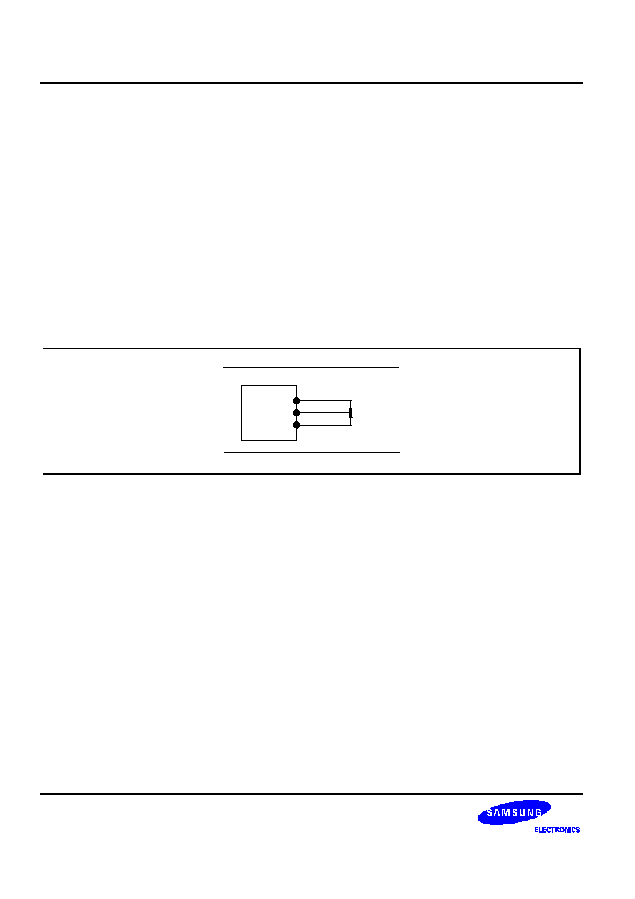
CORE LAYOUT GUIDE
NOTES:
1. The layout of bw0404x consists of digital part and analog part. The digital part and the analog part must be divided.
2. The substrate of digital and analog part is seperated from digital and analog ground so that it can minimize noise
through substrate.
3.
It is recommended that you use thick analog power metal. when connecting to PAD, and the path should be kept as
short as possible.
4. Digital power and analog power are used separately.
5. When the core block is connected to other blocks, it must be double guardring using N-well and P+active to remove the
substrate and coupling noise. In that case, the power metal should be connected to PAD directly.
6. Digital input signal lines must be same length to reduce the difference of delay.
Left VDDA and right VDDA are tied to one PAD separately.
Left VSSA and right VSSA are tied to one PAD separately.
Example
PAD
Metal
CORE

BW0404X
0.5
µ
µ
M SIGMA-DELTA ADC
9
FEEDBACK REQUEST
Sigma-Delta
ADC
Specification
We appreciate your interest in our products. If you have further questions, please specify in the attached form.
Thank you very much.
Parameter
Min
Typ
Max
Unit
Remarks
Supply voltage
V
Max master clock frequency
Hz
Operating temperature
∞
C
Sampling Frequency
Hz
ADC
Dynamic range
dB
Total harmonic distortion
dB
Signal-to-noise ratio
dB
Output format resolution (Serial/Parallel
interface)
Bit
Channel
Mono
Stereo
Power dissipation
mW
Input voltage range
Vpp
ADC offset error
V
ADC group delay
sec
Phase linearity deviation for passband
region
∞
(Deg)
Peak-to-peak frequency response ripple
for passband region
dB
Could
you
explain
external/internal
pin
configurations
as
required?
Specially
requested
function
list
:

0.5
µ
µ
M SIGMA-DELTA ADC
BW0404X
10
NOTES