 | –≠–ª–µ–∫—Ç—Ä–æ–Ω–Ω—ã–π –∫–æ–º–ø–æ–Ω–µ–Ω—Ç: bw1220X | –°–∫–∞—á–∞—Ç—å:  PDF PDF  ZIP ZIP |

0.35
µ
µ
µ
µ
m CCD SIGNAL PROCESSOR FOR CAMCORDER
BW1220X
1
GENERAL
DESCRIPTION
The BW1220X is complete CCD and video signal processor for digital cameras. It converts the analog input signal into
10-bit binary digital codes at a maximum sampling rate of 12MHz. The BW1220X includes CDS(Correlated Double
Sampler), PGA(Programmable Gain Amplifier), clamp for video input, and 10-bit analog to digital converter with
reference generator.
APPLICATIONS
-- Digital Camcorder
-- Still Camera
FEATURES
-- Integrated Correlated Double Sampler
-- Analog Programmable Gain Amplifier (gain step: 0.156, gain range: 0.156 - 40 time)
-- Video Input available
-- Internal Voltage Reference
-- No Missing Code Guaranteed
-- Operation by 3.3V Single Power Supply
-- 64 QFP Package

BW1220X
0.35
µ
µ
µ
µ
m CCD SIGNAL PROCESSOR FOR CAMCORDER
2
FUNCTIONAL BLOCK DIAGRAM
CDS
PGA
MUX
BandGap
Clock
Video Buffer
CLAMP
10 b ADC
RPGA
VIDEOIN
S
ELI
N
SH
D
CL
P1
RE
FT
RE
FB
CO
M
SD
I
8 b
10 b
DO[9:0]
SH
P
SC
SN
SC
L
K
CLAMP
PG
CLAMP
DG
PBLK
CLP4
BG
R
MCLK
MO
DE
Serial to parallel
converter
PD
OE
N
DS
DP[7:0]
VB
B
VS
S
C
VDDC
VS
S
A
VDD
A
VS
S
D
VDDD

0.35
µ
µ
µ
µ
m CCD SIGNAL PROCESSOR FOR CAMCORDER
BW1220X
3
CORE
PIN
DESCRIPTION
Name
I/O Type
I/O Pad
Pin Description
SCLK
DI
picc_bb
External clock forserial gain control input
DS
DI
picc_bb
Serial PGA gain control input
SDI
DI
picc_bb
PGA gain control select (low for serial input)
SCSN
DI
picc_bb
Serial gain control input enble(active low)
CLP1
DI
picc_bb
Black level restore clamp(active high)
DP[0]
DI
picc_bb
Parallel PGA gain control input
DP[1]
DI
picc_bb
Parallel PGA gain control input
DP[2]
DI
picc_bb
Parallel PGA gain control input
DP[3]
DI
picc_bb
Parallel PGA gain control input
DP[4]
DI
picc_bb
Parallel PGA gain control input
DP[5]
DI
picc_bb
Parallel PGA gain control input
DP[6]
DI
picc_bb
Parallel PGA gain control input
DP[7]
DI
picc_bb
Parallel PGA gain control input
SHP
DI
picc_bb
Reference sample clock input
SHD
DI
picc_bb
Data Sample clock input
MCLK
DI
picc_bb
External clock for ADC
MODE
DI
picc_bb
Clock select (high MCLK)
CLP4
DI
picc_bb
Input clamp (Active High)
PG
AI
piar10_bb
CDS input (AC coupled CCD output through 1uF)
DG
AI
piar10_bb
CDS input (AC coupled CCD output through 1uF)
SELIN
DI
picc_bb
Analog input select(low CCD output)
VIDEOIN
AI
piar10_bb
Composite video input
PD
DI
picc_bb
Power down (active high)
BGR
AO
poar50_bb
Bandgap output voltage
IOUT
AO
poar50_bb
Current output for testing
IVB
AO
poar50_bb
Bias current control for testing
COM
AO
poa_bb
Common mode level
REFT
AO
poa_bb
Reference top voltage
REFB
AO
poa_bb
Reference bottom voltage
PBLK
DI
picc_bb
Pixel blanking control(Active Low)
OEN
DI
picc_bb
control input enable

BW1220X
0.35
µ
µ
µ
µ
m CCD SIGNAL PROCESSOR FOR CAMCORDER
4
CORE
PIN
DESCRIPTION (Continued)
Name
I/O Type
I/O Pad
Pin Description
DO[0]
DO
pot4_bb
Digital output
DO[1]
DO
pot4_bb
Digital output
DO[2]
DO
pot4_bb
Digital output
DO[3]
DO
pot4_bb
Digital output
DO[4]
DO
pot4_bb
Digital output
DO[5]
DO
pot4_bb
Digital output
DO[6]
DO
pot4_bb
Digital output
DO[7]
DO
pot4_bb
Digital output
DO[8]
DO
pot4_bb
Digital output
DO[9]
DO
pot4_bb
Digital output
I/O Type Abbr.
-- AI: Analog Input
-- DI: Digital Input
-- AO: Analog Output
-- DO: Digital Output
-- AB: Analog Bidirectional
-- DB: Digital Bidirectional
-- AP: Analog Power
-- DP: Digital Power
-- AG: Analog Ground
-- DG: Digital Ground

0.35
µ
µ
µ
µ
m CCD SIGNAL PROCESSOR FOR CAMCORDER
BW1220X
5
CODE CONFIGURATION
SE
LI
N
CL
P1
SC
S
N
RE
FT
RE
FB
CO
M
VS
S
D
SH
D
VDDD
SC
L
K
DG
IO
UT
SH
P
BG
R
SD
I
DS
bw1220X
PD
PG
DO[9:0]
V
SSA
VDDA
MO
DE
MC
LK
PB
L
K
DP[7:0]
VDDC
VSSC
VIDE
O
I
N
IV
B
VBB
CLP4
OE
N

BW1220X
0.35
µ
µ
µ
µ
m CCD SIGNAL PROCESSOR FOR CAMCORDER
6
ABSOLUTE MAXIMUM
RATINGS
Characteristic
Symbol
Value
Unit
Supply Voltage
VDD
4.5
V
Analog Input Voltage
DP/DG/VIDEOIN
VSS to VDD
V
Digital Input Voltage
SHP/SHD
VSS to VDD
V
Digital Output Voltage
VOH,VOL
VSS to VDD
V
Reference Voltage
REFT/REFB/COM/BGR
VSS to VDD
V
Storage Temperature Range
Tstg
-45 to 150
°…
Operating Temperature Range
Topr
0 to 70
°…
NOTES:
1.
ABSOLUTE
MAXIMUM
RATING
specifies
the
values
beyond
which
the
device
may
be
damaged
permanently.
Exposure
to
ABSOLUTE
MAXIMUM
RATING
conditions
for
extended
periods
may
affect
reliability.
Each
condition
value
is
applied
with
the
other
values
kept
within
the
following
operating
conditions
and
function
operation
under
any
of
these
conditions
is
not
implied.
2.
All
voltages
are
measured
with
respect
to
VSS
unless
otherwise
specified.
3.
100pF
capacitor
is
discharged
through
a
1.5k
resistor
(Human
body
model)

0.35
µ
µ
µ
µ
m CCD SIGNAL PROCESSOR FOR CAMCORDER
BW1220X
7
ANALOG SPECIFICATIONS
Characteristics
Symbol
Min
Typ
Max
Unit
Conditions
Resolution
10
bits
CDS
Maximum Input Range
Maximum Pixel Rate
≠
≠
1.4
12
≠
≠
≠
≠
≠
V
MSPS
PGA
Gain Range min
Gain Range max
Gain Step
≠
≠
≠
≠
38
≠
≠
≠
0.156
0.3
≠
≠
time
time
time
Ain=1Vpp
Gain=2
ADC
Differential
Nonlinearity
DNL
-
-
°æ1
LSB
Integral
Nonlinearity
INL
-
°æ1.5
LSB
Maximum Conversion
Rate
fc
12
-
-
MSPS
Reference Top Reference
Bottom
REFT
REFB
≠
≠
2.0
1.0
≠
≠
V
V
Power Supply
Analog Voltage
Digital Voltage
Analog Current
Digital Current
VDDA
VDDD
IDDA
IDDD
3.3
3.3
50
10
V
V
mA
mA
Power Consumption
200
250
mW

BW1220X
0.35
µ
µ
µ
µ
m CCD SIGNAL PROCESSOR FOR CAMCORDER
8
DIGITAL SPECIFICATIONS
Characteristics
Symbol
Min
Typ
Max
Unit
Conditions
Logic Input
High Level Input Voltage
Low Level Input Voltage
High Level Input Current
Low Level Input Current
Input Capacitance
VIH
VIL
IIH
IIL
CIN
VDD-0.5
≠
≠
≠
≠
≠
≠
10
10
5
≠
VSS+|
0.5
≠
≠
≠
V
V
uA
uA
pF
Logic Output
High Level Output Voltage
Low Level Output Voltage
High Level Input Current
Low Level Input Current
VOH
VOL
IOH
IOL
VDD-0.5
≠
≠
≠
≠
≠
100
100
≠
VSS+|
0.5
≠
≠
V
V
uA
uA
TIMING SPECIFICATIONS
Characteristics
Symbol
Min
Typ
Max
Unit
SHP Clock Period
≠
83
≠
≠
ns
SHD Clock Period
≠
83
≠
≠
ns
SHP Clock High Period
≠
≠
63
≠
ns
SHP Clock Low Period
≠
≠
20
≠
ns
SHD Clock High Period
≠
≠
63
≠
ns
SHD Clock Low Period
≠
≠
20
≠
ns
ADC Clock Period
≠
83
≠
≠
ns
ADC Clock High Period
≠
≠
41.5
≠
ns
ADC Clock Low Period
≠
≠
41.5
≠
ns
Digital Output Delay
t
d
5
10
ns
0.35
µ
µ
µ
µ
m CCD SIGNAL PROCESSOR FOR CAMCORDER
BW1220X
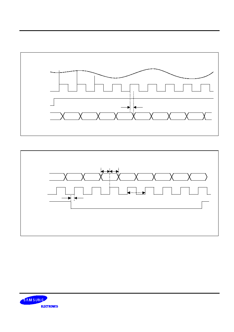
9
TIMING
DIAGRAM
External or
Internal
Clock
Video
Input
A(0)
A(1)
A(2)
D(-3)
D(-2)
D(-1)
D(0)
D(1)
D(2)
D(3)
Digital
Output
SELIN
t
d
D7
D6
D5
D4
D3
D2
D1
D0
SCLK
SCSN
DS
t
ha
t
sa
t
sa
= 4ns(min);t
ha
= 4ns(min)
t
sclk
= 100ns(min)
t
sclk
t
sa
BW1220X
0.35
µ
µ
µ
µ
m CCD SIGNAL PROCESSOR FOR CAMCORDER
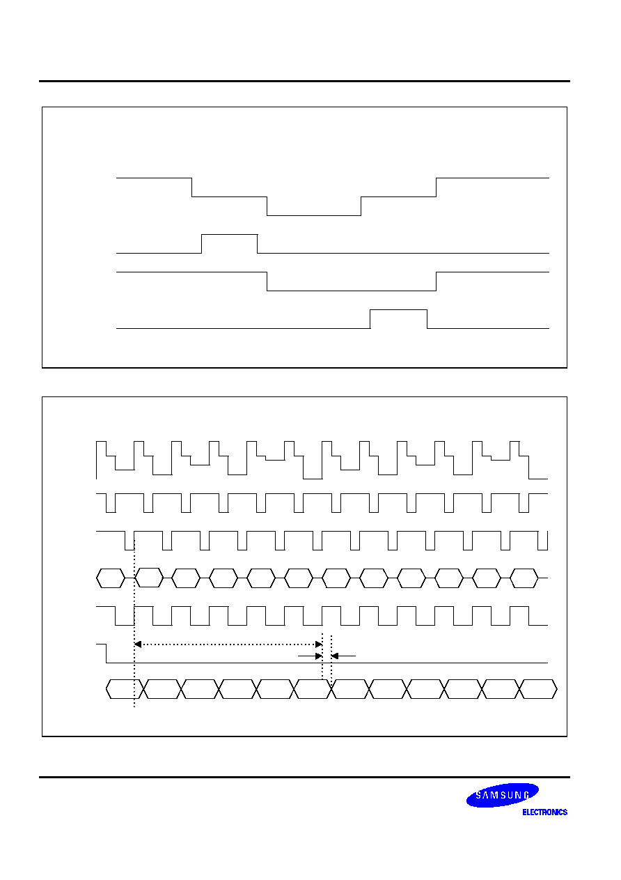
10
CCD
Output
Effective
pixel interval
Optical
Black
interval
Horizontal
flyback
interval
Optical
Dummy
interval
Effective pixel
interval
CLP1
PBLK
CLP4
N
N+1
N+2
N+3
CCD
Outpu
t
SHP
SHD
Internal
CLK
CDS
Outpu
t
N+1
N+2
N+3
N+4
N+5
N+6
N+7
N+8
N+9
Digital
Outpu
t
N
N-1
N-2
N-3
N-4
N+1
N+2
N+3
N+4
N+5
MODE
N-5
Latency
t
d
N
0.35
µ
µ
µ
µ
m CCD SIGNAL PROCESSOR FOR CAMCORDER
BW1220X
11
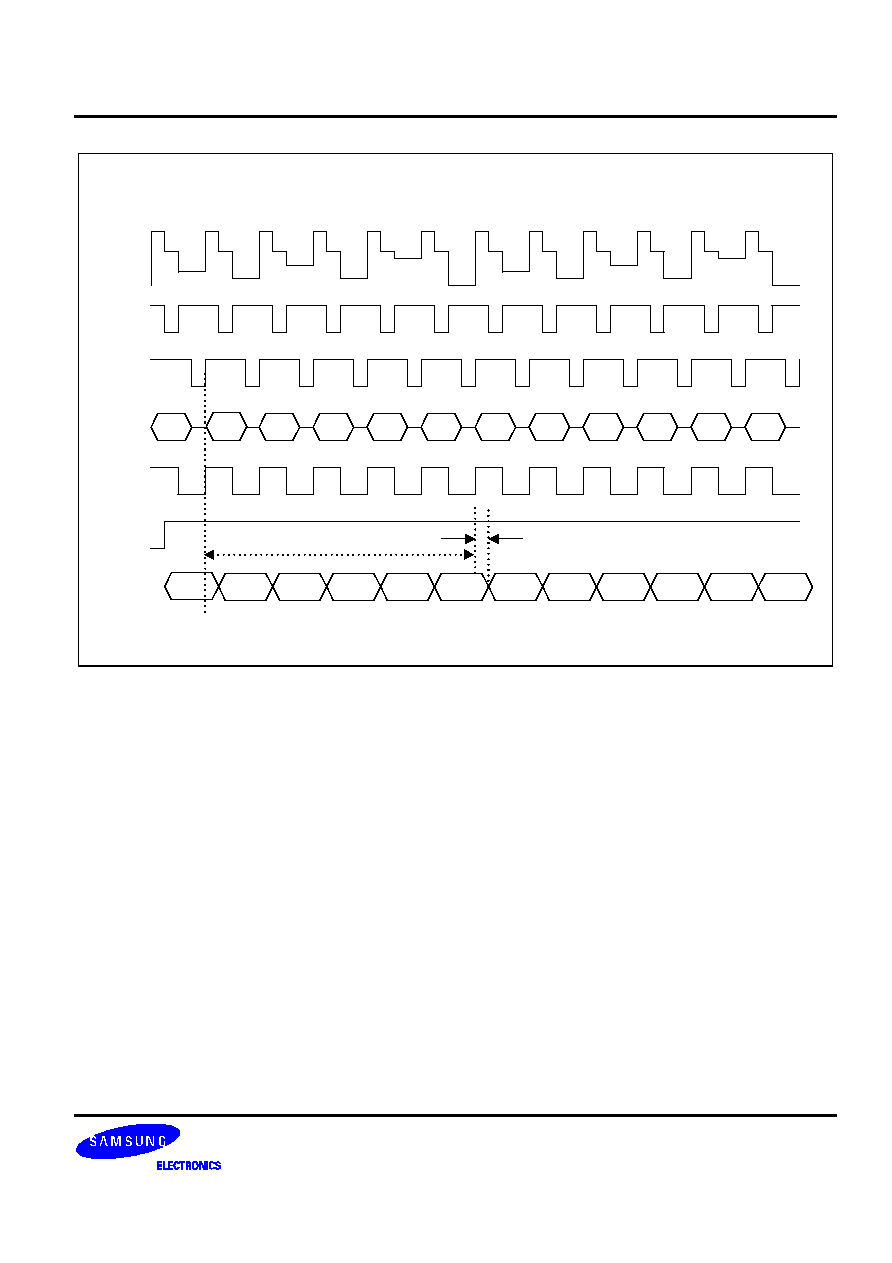
N
N+1
N+2
N+3
CCD
Output
SHP
SHD
External
CLK
CDS
Output
N+1
N+2
N+3
N+4
N+5
N+6
N+7
N+8
N+9
Digital
Output
N
N-1
N-2
N-3
N-4
N+1
N+2
N+3
N+4
N+5
MODE
N-5
Latency
t
d
N

BW1220X
0.35
µ
µ
µ
µ
m CCD SIGNAL PROCESSOR FOR CAMCORDER
12
CORE EVALUATION GUIDE
1. BW1220X is evaluated by external check on the bidirectional pads connected to input nodes of DSP back-end
circuit.
2. The reference voltages may be biased externally through REFT , REFB and COM pins, otherwise these
voltages are internally generated at Reference Voltage Block (Bandgap).
CLP
1
SC
S
N
RE
FB
RE
FT
PD
VS
SD
SH
D
VD
DD
SC
L
K
VDDC
DG
IO
U
T
SH
P
COM
SD
I
DS
bw1220X
IV
B
PG
DO[9:0]
MUX
HOST
DSP
CORE
BIDIRECTIONAL PAD FOR
TESTING
DO[9:0]
10u
0.1u
0.
1u
0.
1u
0.
1u
10u
0.
1u
VD
D
A
VS
SA
MCLK
MODE
DI[9:0]
D
P
[7
:0]
P
BLK
VSSC
VBB
CLP4
BG
R
S
ELIN
VI
DEOI
N
OE
N

0.35
µ
µ
µ
µ
m CCD SIGNAL PROCESSOR FOR CAMCORDER
BW1220X
13
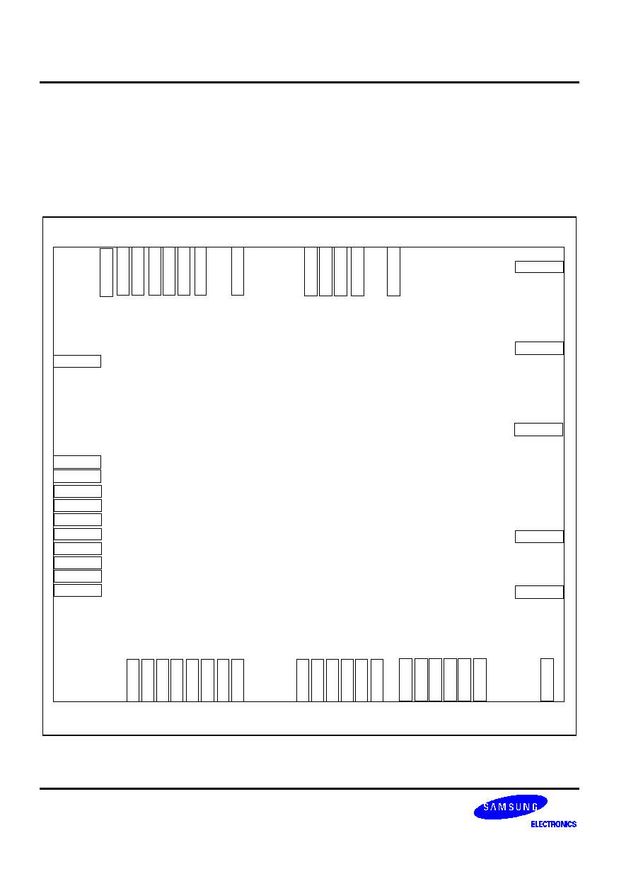
PACKAGE CONFIGURATION
BW1220X
DP[3]
DP[2]
DP[0]
DO[9]
DO[8]
DO[7]
DO[6]
DO[5]
DO[4]
DO[3]
DO[2]
DO[1]
DO[0]
VDDP
VSSP
DP[1]
CLP4
NC
R1
VBB
VBB
VSSC
VSSC
PG
DG
VDDC
VDDC
NC
NC
NC
NC
NC
DP[4]
DP[5]
DP[6]
DP[7]
PB
L
K
VS
S
D
VD
DD
SC
L
K
DS
SD
I
SC
SN
CL
P1
SH
D
SH
P
MC
LK
MO
D
E
OEN
V
SSA
VDD
A
REFT
REFB
V
SSA
V
SSA
SEL
I
N
VDD
A
VDD
A
PD
COM
BGR
IVB
IOUT
VID
E
OIN
VDDA
DG
PG
Video in
10u
0.1
u
10u
0.
1
u
10u
0.1
u
10
u
0.1
u
10
K
0.
1
u
0.
1
u
0.
1
u 10 u
0.1
u
10
u
50
0.1
u
0.1
u
1u
1u
BW1220X
0.35
µ
µ
µ
µ
m CCD SIGNAL PROCESSOR FOR CAMCORDER
14
PACKAGE PIN DESCRIPTION
Name
Pin No.
I/O Type
Pin Description
DP[4]
1
DI
Parallel PGA gain control input
DP[5]
2
DI
Parallel PGA gain control input
DP[6]
3
DI
Parallel PGA gain control input
DP[7]
4
DI
Parallel PGA gain control input
PBLK
5
DI
Pixel blanking control (Active Low)
VSSD
6
DG
Internal digital Ground
VDDD
7
DP
Internal digital Supply
SCLK
8
DI
External clock for serial gain control input
DS
9
DI
Serial PGA gain control input
SDI
10
DI
PGA gain control select (low for serial input)
SCSN
11
DI
Serial gain control input enble
CLP1
12
DI
Black level restore clamp (active high)
SHD
13
DI
Data sample clock input
SHP
14
DI
Reference sample clock input
MCLK
15
DI
External clock for ADC
MODE
16
DI
Clock select (high MCLK)
CLP4
17
DI
Input clamp (active high)
NC
18
≠
≠
NC
19
≠
≠
R1
20
≠
Chip I.D.
VBB
21
AG
Substrate Ground
VBB
22
AG
Substrate Ground
VSSC
23
AG
Analog Ground
VSSC
24
AG
Analog Ground
PG
25
AI
CDS input (AC coupled CCD output through 1uF)
DG
26
AI
CDS input (AC coupled CCD output through 1uF)
VDDC
27
AP
Analog Supply
VDDC
28
AP
Analog Supply
NC
29
≠
≠
NC
30
≠
≠
NC
31
≠
≠
NC
32
≠
≠

0.35
µ
µ
µ
µ
m CCD SIGNAL PROCESSOR FOR CAMCORDER
BW1220X
15
PACKAGE PIN DESCRIPTION (Continued)
Name
Pin No.
I/O Type
Pin Description
IOUT
33
AO
Current output for testing
BGR
34
AO
Bandgap output Voltage
IVB
35
AO
Bias current control for testing
COM
36
AO
Common mode level
PD
37
DI
Power down (active high)
SELIN
38
DI
Analog input select (low CCD output)
VIDEOIN
39
AI
Composite video input
VDDA
40
AP
Analog Supply
VDDA
41
AP
Analog Supply
VSSA
42
AG
Analog Ground
VSSA
43
AG
Analog Ground
REFT
44
AO
Reference top voltage
REFB
45
AO
Reference bottom voltage
VDDA
46
AP
Analog Supply
VSSA
47
AG
Analog Ground
OEN
48
DI
Digital output enble (active low)
VSSP
49
PG
Digital Ground for output buffer
VDDP
50
PP
Digital Supply for output buffer
DO[0]
51
DO
Digital output(LSB)
DO[1]
52
DO
Digital output
DO[2]
53
DO
Digital output
DO[3]
54
DO
Digital output
DO[4]
55
DO
Digital output
DO[5]
56
DO
Digital output
DO[6]
57
DO
Digital output
DO[7]
58
DO
Digital output
DO[8]
59
DO
Digital output
DO[9]
60
DO
Digital output(MSB)
DP[0]
61
DI
Parallel PGA gain control input
DP[1]
62
DI
Parallel PGA gain control input
DP[2]
63
DI
Parallel PGA gain control input
DP[3]
64
DI
Parallel PGA gain control input
NOTE: I/O type PP and PG denote PAD power and PAD ground respectively.
BW1220X
0.35
µ
µ
µ
µ
m CCD SIGNAL PROCESSOR FOR CAMCORDER
16
PHANTOM CELL INFORMATION
-- Pins of the core can be assigned externally (Package pins) or internally (internal ports) depending on design
methods.
The term "External" implies that the pins should be assigned externally like power pins.
The term "External/internal" implies that the applications of these pins depend on the user.
BW1220X
CCD Signal Processor for Camcorder
V
D
D
A
R
E
F
B
R
E
F
T
DG
VBB
VDDC
PG
VSSC
V
S
S
A
V
D
D
A
V
D
-
I
N
-
S
E
L
I
N
DO[0]
VSSA
DO[1]
P
D
C
O
M
I
V
B
B
G
R
I
O
U
T
S
C
S
N
C
L
P
1
S
H
D
S
H
P
M
C
L
K
M
O
D
E
C
L
P
4
P
B
L
K
V
S
S
D
V
D
D
D
S
C
L
K
D
S
S
D
I
D
P
[
5
]
D
P
[
6
]
D
P
[
7
]
D
P
[
0
]
D
P
[
1
]
D
P
[
2
]
D
P
[
3
]
D
P
[
4
]
DO[2]
DO[3]
DO[4]
DO[5]
DO[6]
DO[7]
DO[8]
DO[9]
O
E
N

0.35
µ
µ
µ
µ
m CCD SIGNAL PROCESSOR FOR CAMCORDER
BW1220X
17
Pin Name
Pin Usage
Pin Layout Guide
VDDA
External
- Maintain the large width of lines as far as the pads.
- place the port positions to minimize the length of power lines.
- Do not merge the analog powers with anoter power from other blocks.
- Use good power and ground source on board.
VSSA
External
VBB
External
VDDD
External
VSSD
External
VDDC
External
VSSC
External
VIDEOIN
External/Internal
- Do not overlap with digtal lines.
- Maintain the shotest path to pads.
SCLK
External/Internal
- Separate from all other analog signals
NCLK
External/Internal
REFT
External/Internal
- Maintain the larger width and the shorter length as far as the pads.
- Separate from all other digital lines.
REFB
External/Internal
PD
External/Internal
SELIN
External/Internal
COM
External/Internal
DG
External/Internal
PG
External/Internal
MODE
External/Internal
CLP4
External/Internal
SHP
External/Internal
SHD
External/Internal
CLP1
External/Internal
SCSN
External/Internal
SDI
External/Internal
DS
External/Internal
PBLK
External/Internal
BGR
External/Internal
- Separate from all other digital signals
IOUT
External/Internal
IVB
External/Internal
DP[0] - DP[7]
External/Internal
- Separated from the analog clean signals if possible.
- Do not exceed the length by 1,000um.
D0[0] - D0[9]
External/Internal

BW1220X
0.35
µ
µ
µ
µ
m CCD SIGNAL PROCESSOR FOR CAMCORDER
18
FEEDBACK REQUEST
It should be quite helpful to our ADC core development if you specify your system requirements on ADC in the
following characteristic checking table and fill out the additional questions.
We appreciate your interest in our products. Thank you very much.
Characteristic
Min
Typ
Max
Unit
Remarks
Analog Power Supply Voltage
V
Digital Power Supply Voltage
V
Bit Resolution
Bit
Reference Input Voltage
V
Analog Input Voltage
Vpp
Operating Temperature
∞
C
Integral Non-linearity Error
LSB
Differential Non-linearity Error
LSB
Bottom Offset Voltage Error
mV
Top Offset Voltage Error
mV
Maximum Conversion Rate
MSPS
Dynamic Supply Current
mA
Power Dissipation
mW
Signal-to-noise Ratio
dB
Pipeline Delay
CLK
Digital Output Format
(Provide detailed description &
timing diagram)
1. Between single input-output and differential input-output configurations, which one is suitable for your system
and why?
2. Please comment on the internal/external pin configurations you want our ADC to have, if you have any reason
to prefer some type of configuration.
3. Freely list those functions you want to be implemented in our ADC, if you have any.

0.35
µ
µ
µ
µ
m CCD SIGNAL PROCESSOR FOR CAMCORDER
BW1220X
19
HISTORY CARD
Version
Date
Modified Items
Comments
Ver 1.0
00.1.30
Original version published (preliminary)
BW1220X
Ver 2.0
02.4.23
Phantom cell information added
BW1220X

BW1220X
0.35
µ
µ
µ
µ
m CCD SIGNAL PROCESSOR FOR CAMCORDER
20
NOTES