 | –≠–ª–µ–∫—Ç—Ä–æ–Ω–Ω—ã–π –∫–æ–º–ø–æ–Ω–µ–Ω—Ç: bw1222l | –°–∫–∞—á–∞—Ç—å:  PDF PDF  ZIP ZIP |

0.35
µ
µ
µ
µ
m AFE FOR CCD/CIS SIGNAL PROCESSOR
BW1222L
1
GENERAL
DESCRIPTION
The samsung analog front end(AFE) for CCD/CIS image signal is an integrated analog signal processor for color
image signal.
The AFE converts CCD/CIS output signal to digital data. The AFE includes three-channel CDS(Correlated Double
Sampler) circuit, PGA(Programmable Gain Amplifier), and 10-bit analog to digital converter with reference
generator.
A parallel data bus provides a simple interface to 8-bit microcontroller.
APPLICATIONS
-- Color and B/W Scanner
-- Digital Copiers
-- Facsimile
-- General Purpose CCD/CIS imager
FEATURES
-- 10-bit 6MSPS A/D Converter
-- Integrated Triple Correlated Double Sampler
-- 3-Channel 2 MSPS Color Mode
-- Analog Programmble Gain Amplifier
-- Internal Voltage Reference
-- Wide clamp level controllability for CIS signal
-- No Missing Code Guaranteed
-- Microcontroller-Compatible Control Interface
-- Operation by 3.3V Power Supply
-- CMOS Low Power Dissipation
KEY
SPECIFICATION
-- Resolution: 10-bit
-- Conversion Rate: 6 MHz(2 MHz*3)
-- Supply Voltage: 3.3 V ± 5%
-- Power Dissipation: 250 mW(Typical)
BW1222L
0.35
µ
µ
µ
µ
m AFE FOR CCD/CIS SIGNAL PROCESSOR
2
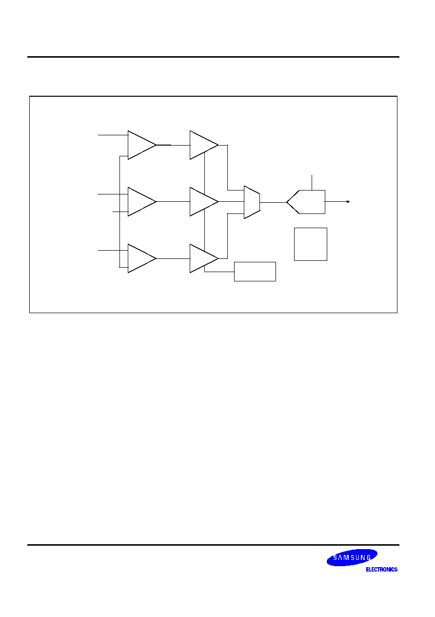
FUNCTIONAL BLOCK DIAGRAM
CDS
CDS
CDS
PGA
PGA
PGA
MUX
GAIN
REGISTER
INPUT OFFSET
REGISTER
ADC
REF
MPU
PORT
RED
GREEN
BLUE
D[9:0]
0.35
µ
µ
µ
µ
m AFE FOR CCD/CIS SIGNAL PROCESSOR
BW1222L
3
CORE
PIN
DESCRIPTION
Name
I/O Type
I/O Pad
Description
VDDA1, VDDA2
AP
vdda
Analog Supply
VSSA1, VSSA2
AG
vssa
Analog Ground
VBB
AG
vbba
Analog Bulk
REFT
AB
pia_bb
Reference Decoupling
REFB
AB
pia_bb
Reference Decoupling
VCOM
AB
pia_bb
Analog Common Voltage
R_VIN
AI
piar10_bb
Analog Input; Red
G_VIN
AI
piar10_bb
Analog Input; Green
B_VIN
AI
piar10_bb
Analog Input; Blue
STRTLN
DI
picc_bb
STRTLN indicates beginning of line
CDS1_CLK
DI
picc_bb
CDS Reset Clock Pulse Input
CDS2_CLK
DI
picc_bb
CDS Data Clock Pulse Input
ADCCLK
DI
picc_bb
A/D Converter Sample Clock Input
VDDA3
DP
vddd
Digital Supply (2 pins;VDDA3, VDDA4)
VSSA3
DG
vssd
Digital Ground (2 pins;VSSA3, VSSA4)
CSB
DI
picc_bb
Chip Select; Active Low
WRB
DI
picc_bb
Write Strobe; Active Low
RDB
DI
picc_bb
Read Strobe; Active Low
OEB
DI
picc_bb
Output Enable; Active Low
D[9:0]
DB
poa_bb
Data Inputs/Outputs
AD[2:0]
DI
picc_bb
Register Select
TEST_S1, TEST_S2
DI
picc_bb
Channel Select in Test Mode
TEST_CTL
DI
picc_bb
Test Mode Control; Active Low
TEST_OUT
AO
poa_bb
Test Mode Output
MCTL1, MCTL2
DI
picc_bb
Channel Select in External MUX Control
EXT_MCTL
DI
picc_bb
External MUX Control; Active Low
I/O Type Abbr.
-- AI: Analog Input
-- DI: Digital Input
-- AO: Analog Output
-- DO: Digital Output
-- AB: Analog Bidirectional
-- DB: Digital Bidirectional
-- AP: Analog Power
-- DP: Digital Power
-- AG: Analog Ground
-- DG: Digital Ground

BW1222L
0.35
µ
µ
µ
µ
m AFE FOR CCD/CIS SIGNAL PROCESSOR
4
CODE CONFIGURATION
bw1222l
R_VIN
ADCCLK
MCTL1,MCTL2
D[9:0]
REFT
AD[2:0]
CSB
WRB
RDB
OEB
EXT_MCTL
TEST_S1,TESTS2
TEST_OUT
CDS2_CLK
CDS1_CLK
STRTLN
G_VIN
R_VIN
B_VIN
R_VIN
VCOM
REFB
VDDA1,VDDA2
VSSA1,VSSA2,VBBA
VDDA3,VDDA4
VSSA3,VSSA4
TEST_CTL
2
2
10
3
3
2
2
2
ABSOLUTE MAXIMUM
RATINGS
Characteristics
Symbol
Value
Unit
Supply Voltage
VDD
4.5
V
Analog Input Voltage
AIN
VSS to VDD
V
Digital Input Voltage
CLK
VSS to VDD
V
Reference Voltage
VRT/VRB
VSS to VDD
V
Storage Temperature Range
Tstg
-45 to 150
∞
C
Operating Temperature Range
Topr
0 to 70
∞
C
NOTES:
1.
ABSOLUTE
MAXIMUM
RATING
specifies
the
values
beyond
which
the
device
may
be
damaged
permanently.
Exposure
to
ABSOLUTE
MAXIMUM
RATING
conditions
for
extended
periods
may
affect
reliability.
Each
condition
value
is
applied
with
the
other
values
kept
within
the
following
operating
conditions
and
function
operation
under
any
of
these
conditions
is
not
implied.
2.
All
voltages
are
measured
with
respect
to
VSS
unless
otherwise
specified.
3.
100pF
capacitor
is
discharged
through
a
1.5k
resistor
(Human
body
model)
0.35
µ
µ
µ
µ
m AFE FOR CCD/CIS SIGNAL PROCESSOR
BW1222L
5
ANALOG SPECIFICATIONS
(VDDA1, VDDA2=3.3V, VDDA3=3.3V, ADCCLK=6MHz, CDS1_CLK=2MHz,CDS2_CLK=2MHz, PGA Gain=1
unless otherwise noted)
Characteristics
Symbol
Min
Typ
Max
Unit
Comment
Resolution
10
Bits
Signal-to-Noise &
Distortion Ratio
SNDR
46
49
dB
Conversion Rate
3-Channel with CDS
1-Channel with CDS
6
6
MSPS
MSPS
Differential
Nonlinearity
DNL
±
1
LSB
Integral
Nonlinearity
INL
±
2
LSB
Unipolar Offset Error
0.8
%FSR
Gain Error
1.6
%FSR
Anlog Input
Full-Scale Input
Input Capacitance
Reference Top
Reference Bottom
0.06
8
2.1
1.1
2.0
Vp-p
pF
V
V
Power Supply
Analog Voltage
Digital Voltage
Analog Current
Digital Current
VDDA
VDDD
IDDA
IDDD
3.15
3.15
3.3
3.3
70
5
3.45
3.45
V
V
mA
mA
3.3V
±
5%
3.3V
±
5%
Power Consumption
250
mW
Temperature Range
0
70
∞
C
DIGITAL SPECIFICATIONS
(VDDA1, VDDA2=3.3V, VDDA3=3.3V, ADCCLK=6MHz, CDS1_CLK=2MHz, CDS2_CLK=2MHz, C
L
=20pF
unless otherwise noted)
Characteristics
Symbol
Min
Typ
Max
Unit
Comment
High
Level
Input
Voltage
V
IH
2.0
V
Low
Level
Input
Voltage
V
IL
0.8
V
High
Level
Input
Current
I
IH
10
mA
Low
Level
Input
Current
I
IL
10
mA
High
Level
Output
Voltage
V
oH
2.4
V
I
oH
=0.5mA
Low
Level
Output
Voltage
V
OL
0.4
V
I
oL
=-0.5mA

BW1222L
0.35
µ
µ
µ
µ
m AFE FOR CCD/CIS SIGNAL PROCESSOR
6
TIMING SPECIFICATIONS
Characteristics
Symbol
Min
Typ
Max
Unit
3-Channel Conversion Rate
500
ns
1-Channel Conversion Rate
166
ns
CDS1_CLK Pulse Width
t
C1CLK
60
ns
CDS2_CLK Pulse Width
t
C2CLK
70
ns
CDS2_CLK2 Pulse Width
t
C2CLKB
70
ns
CDS1_CLK Falling to
CDS2_CLK2Rising
t
C1C2A
5
ns
CDS2_CLK Falling to CDS1_CLK
Rising
t
C2C1A
5
ns
ADCCLK Pulse Width
t
ADCLK
70
ns
CDS2_CLK Rising to ADCCLK Rising
t
C2ADA
70
ns
CDS2_CLK Falling to ADCCLK Falling
t
C2ADB
5
ns
ADCCLK Rising to CDS2CLK Falling
t
ADC2A
5
ns
STRTLN Rising, Falling Setup & Hold
t
S, tH
15
ns
ADC Output Delay
t
ADDT
20
ns
Register Address Setup Time
t
AS
15
ns
Register Address Hold Time
t
AH
15
ns
Data Hold Time
t
DH
15
ns
Register Chip Select Setup Time
t
CSS
15
ns
Register Chip Select Hold Time
t
CSH
15
ns
Register Read Pulse Width
t
PWR
50
ns
Write Pulse Width
t
PWW
25
ns
Register Read To Data Valid
t
DD
40
ns
Output Enable High to Tri-State
t
HZ
10
ns
Tri-State to Data Valid
t
DEV
15
ns
Aperture Delay
t
AD
2
ns
Latency for 1 Channel mode
3.5
ADCCLK
Cycles
NOTE: Aperture delay is a timing measurement between the sampling clocks and CDS. It is measured from the falling
edge of the CDS2_CLK input to when the input signal is held for data conversion
0.35
µ
µ
µ
µ
m AFE FOR CCD/CIS SIGNAL PROCESSOR
BW1222L
7
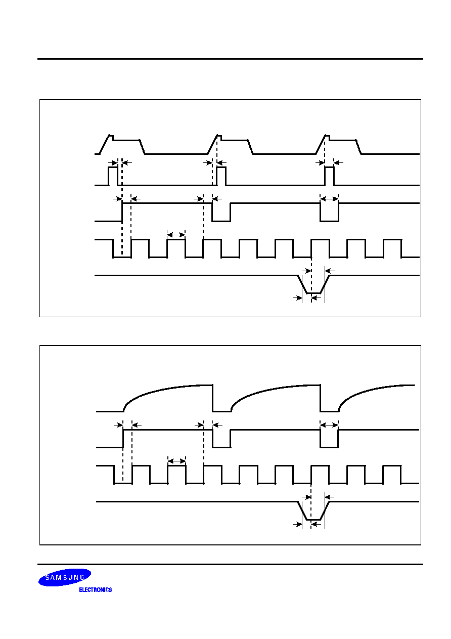
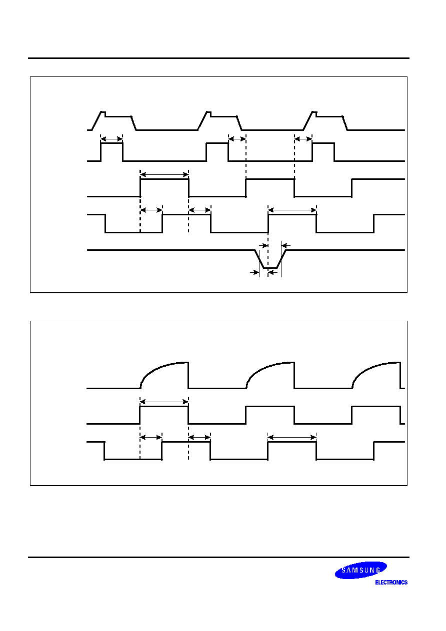
TIMING DIAGRAM
3-CHANNEL
CDS
MODE
Analog
Input
CDS1_CLK
CDS2_CLK
ADCCLK
STRTLN
R0,G0,B0
R1,G1,B1
R2,G2,B2
t
C1C2A
t
C2C1A
t
C1CLK
t
C2ADA
t
ADC2A
t
C2CLKB
t
ADCLK
t
S
t
H
3-CHANNEL
SHA
MODE
Analog
Input
CDS2_CLK
ADCCLK
STRTLN
R0,G0,B0
R1,G1,B1
R2,G2,B2
t
C2ADA
t
ADC2A
t
C2CLKB
t
ADCLK
t
S
t
H
BW1222L
0.35
µ
µ
µ
µ
m AFE FOR CCD/CIS SIGNAL PROCESSOR
8
1-CHANNEL
CDS
MODE
Analog
Input
CDS1_CLK
CDS2_CLK
ADCCLK
t
ADCLK
t
C2ADB
t
C2CLK
t
C1CLK
t
C2ADA
t
C1C2A
t
C2C1A
STRTLN
t
S
t
H
1-CHANNEL
SHA
MODE
Analog
Input
CDS2_CLK
ADCCLK
R0,G0,B0
R1,G1,B1
R2,G2,B2
t
C2CLK
t
ADCLK
t
C2ADB
t
C2ADA

0.35
µ
µ
µ
µ
m AFE FOR CCD/CIS SIGNAL PROCESSOR
BW1222L
9
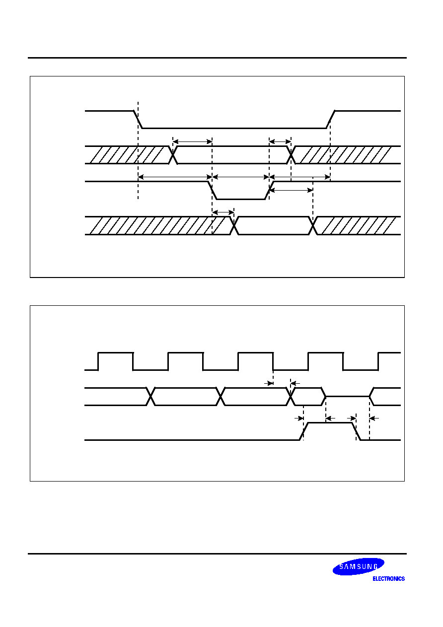
ADC
TIMING
ADC
Input
ADCCLK
ADCOUT
t
ADDT
A(n)
A(n+1)
A(n-2)[9:0]
A(n-1)[9:0]
A(n)[9:0]
WRITE
TIMING
AD[2:0]
WRB
t
AS
t
CSS
CSB
t
AH
D[7:0]
t
PWW
t
DH
t
DD
OEB
t
CSH
BW1222L
0.35
µ
µ
µ
µ
m AFE FOR CCD/CIS SIGNAL PROCESSOR
10
READ(1)
TIMING
AD[2:0]
RDB
t
AS
t
CSS
CSB
t
AH
D[7:0]
t
PWR
t
DH
t
DD
t
CSH
'
Read(1)'
means
microcontroller
reads
D[7:0]/MPU[7:0].
READ(2)
TIMING
ADCCLK
D[9:0]
t
ADDT
OEB
t
HZ
t
DEV
CSB
should
keep
'High'
to
read.

0.35
µ
µ
µ
µ
m AFE FOR CCD/CIS SIGNAL PROCESSOR
BW1222L
11
FUNCTIONAL
DESCRIPTION
1) 3-Channel Operation with CDS
This mode enables simultaneous sampling of a triple output CCD. The CCD waveforms are ac coupled to the
VINR, VING and VINB pins where they are automatically biased at an appropriate voltage using the on-chip clamp.
The internal CDSs take two samples of the incoming pixel data; the first samples are taken during the reset time
while the second samples are taken during data portion of the input pixels. When STRTLN is low, the internal
circuitry is reset on the next rising edge of ADCCLK; the multiplexer is switched to red channel.
2) 3-Channel SHA Operation
This mode enables simultaneous sampling of a triple output CIS or something like that. The CDS functions are
replaced with the sample and hold amplifiers. The input waveforms are either dc coupled or dc restored to the
VINR, VING and VINB pins. The input reference voltage in this mode will be defined by clamp level control
register.
When STRTLN is low, the internal circuitry is reset on the next rising edge of ADCCLK; the multiplexer is switched
to red channel.
3) 1-Channel Operation with CDS
This mode enables single channel or monochrome sampling. The CCD waveforms are ac coupled to the analog
input pin where they are automatically biased at an appropriate voltage using the on-chip clamp.
Bit2 and bit3 in configuration register select the desired input among red, green and blue.
4) 1-Channel SHA Operation
This mode enables single-channel or monochrome sampling. The CDS function is replaced with the sample and
hold amplifier.
The input waveforms are either dc coupled or dc restored to the analog input pin. The input
reference voltage in this mode will be defined by clamp level control register. Bit2 and bit2 in configuration register
select the desired input among red, green and blue.
MAIN
BLOCK
DESCRIPTION
1) Programmable Gain Amplifier
The analog programmable gain can accommodate a wide range of input voltage spans. The transfer function of
the PGA is as follows.
H(X)
=
1/6*X
+
5/6,
where the range of X is 0 to 31.
Thus, the minimum gain value is equal to 5/6, and the maximum gain value is equal to 6. The transfer function has
linearity in linear scale. The overall gain is equal to analog gain multiplied by digital gain. So, the multiplier should
be required in back end of AFE.
2) REGISTER OVERVIEW
The MPU port map is accessed through pins A0, A1 and A2. See MPU port map format.(next page)

BW1222L
0.35
µ
µ
µ
µ
m AFE FOR CCD/CIS SIGNAL PROCESSOR
12
BLOCK
DIAGRAM
Input Offset
Register
(R,G,B)
CDS
PGA
ADC
REF
Gain & Clamp Level
Register
(R,G,B)
Configuration
Register
R_VIN
RED
G_VIN
GREEN
B_VIN
BLUE
CDS1_CLK
CDS2_CLK
ADCCLK
OEB
WRB
AD[2]
D[9:0]/
MPU[7:0]
CSB
MPU
PORT
10
10
VDDA1, 2
VSSA1, 2
VCOM
VDDA3
VSSA3
MCTL2
MCTL1
EXT_MCTL
TEST_S2
TEST_S1
TEST_CTL
TEST_OUT
REFT
REFB
STRTLN
CDS
PGA
CDS
CLAMP
CLAMP
CLAMP
PGA
R_CLAMP[2:0], R_GAIN[4:0]
G_CLAMP[2:0], G_GAIN[4:0]
B_CLAMP[2:0], B_GAIN[4:0]
R_OFFSET[7:0]
G_OFFSET[7:0]
B_OFFSET[7:0]
8
R_OFFSET[7:0]
G_OFFSET[7:0]
B_OFFSET[7:0]
R_CLAMP[2:0]; For only SHA mode
G_CLAMP[2:0]; For only SHA mode
B_CLAMP[2:0]; For only SHA mode
B_GAIN[4:0]
R_GAIN[4:0]
G_GAIN[4:0]
MUX
RDB
AD[1]
AD[0]

0.35
µ
µ
µ
µ
m AFE FOR CCD/CIS SIGNAL PROCESSOR
BW1222L
13
Table 1.
MPU
Port
Map
Format
A2
A1
A0
Register
0
0
0
Configuration
Register
0
0
1
Red
Input
Offset
register
0
1
0
Green
Input
Offset
Register
0
1
1
Blue
Input
Offset
Register
1
0
0
Red
Gain
&
CIS
Clamp
Control
Register
1
0
1
Green
Gain
&
CIS
Clamp
Control
Register
1
1
0
Blue
Gain
&
CIS
Clamp
Control
Register
1
1
1
Reserved
Configuration Register
Bit 7
Bit 6
Bit 5
Bit 4
Bit 3
Bit 2
Bit 1
Bit 0
Clamp
mode
select1
Clamp
mode
select0
Set to 0
External
Reference
Color1
(Single
Channel)
Color0
(Single
Channel)
Single
Channel
CDS
Enable
Single Channel Color Pointer
Bit3
Bit2
Color
0
0
Red
0
1
Green
1
0
Blue
1
1
Reserved
Clamp Mode Selection
Bit3
Bit2
Clamp Mode
0
0
Line Clamp
0
1
Pixel Clamp
1
0
No Clamp
1
1
Reserved

BW1222L
0.35
µ
µ
µ
µ
m AFE FOR CCD/CIS SIGNAL PROCESSOR
14
Input Offset Register
MSB
LSB
Bit 7
Bit 6
Bit 5
Bit 4
Bit 3
Bit 2
Bit 1
Bit 0
Gain & CIS Clamp Control Register
MSB
LSB
Bit 7
Bit 6
Bit 5
Bit 4
Bit 3
Bit 2
Bit 1
Bit 0
PGA2
PGA1
CCC0
PGA4
PGA3
PGA2
PGA1
PGA0
NOTE: CCCn: CIS Clamp Control n.
EXTERNAL MULTIPLEXER CONTROL MODE
EXT_MCTL = "LOW"
MCTL2
MCTL1
Color
0
0
Red
0
1
Green
1
0
Blue
1
1
Reserved

0.35
µ
µ
µ
µ
m AFE FOR CCD/CIS SIGNAL PROCESSOR
BW1222L
15
OVERALL
TRANSFER
FUNCTION
The overall transfer function can be calculated as follows.
ADC
out
=[(Vin+Input_Offset)* PGA_Gain]/(2*REF)*1024,
where REF is equal to (REFT-REFB) and Input _Offset means the DAC value of the input offset register. The
analog offset range of the input offset register is varied between 150mV and -150 mV. The 8-bit data format for
the input offset register is straight binary coding. Thus, an all 'zeros' data word corresponds to -150 mV. An all
'ones' data word corresponds to 150 mV. To maximize the dynamic range of the ADC input, it is necessary to
program the input offset register code to move the ADC code corresponding to the black level towards 'zero'.
In case of processing CIS signal, 3bits of the gain & clamp control register are allocated to control CIS clamp level.
Like the input offset register, the 3-bit data format is straight binary coding. An all 'zeros' data word corresponds to
0.1 V and an all 'ones' data word corresponds to 1.5 V.
INPUT
COUPLING
CAPACITOR
Because of the DC offset present at the output of CCD, some kind of DC restoration is required. In case of CDS
enable mode, to simplify input level shifting, a DC decoupling capacitor is used in conjuction with the internal input
circuitry.
The capacitor charging or discharging depends on the clamping time, the analog input resistance of the AFE and
the output resistance of the circuit driving the coupling capacitor.
The clamping time is typically (n*T), where n is the number of periods CDSCLK1 is asserted and T is the period of
assertion. CDSCLK2 should not be asserted during clamping time. And, STRTLN must be low in line clamp mode
for clamping operation. The analog input resistance of the AFE is equal to 1 kW. The recommended input coupling
capacitor is more than 0.01uF. Thus, to extend the clamping time, the time a transport motor moves the scanner
carriage can be available, for example.

BW1222L
0.35
µ
µ
µ
µ
m AFE FOR CCD/CIS SIGNAL PROCESSOR
16
TEST
MODE
FOR
EACH
PGA
OUTPUT
(OPTIONAL)
It is possible to test each PGA output that is connected to next ADC block by external control pins. So, each PGA
output can be shown with an external test pin.
Test mode control(TEST_CTL) pin should go 'LOW' to operate AFE in test mode.
Color Pointer for Test Mode
TEST_S2
TEST_S1
Color
0
0
Red
0
1
Green
1
0
Blue
1
1
Reserved
PGA
ADC
R
G
B
TEST MUX
<TEST_CTL>
<TEST_S2>
<TEST_S1>
<TEST_OUT>

0.35
µ
µ
µ
µ
m AFE FOR CCD/CIS SIGNAL PROCESSOR
BW1222L
17
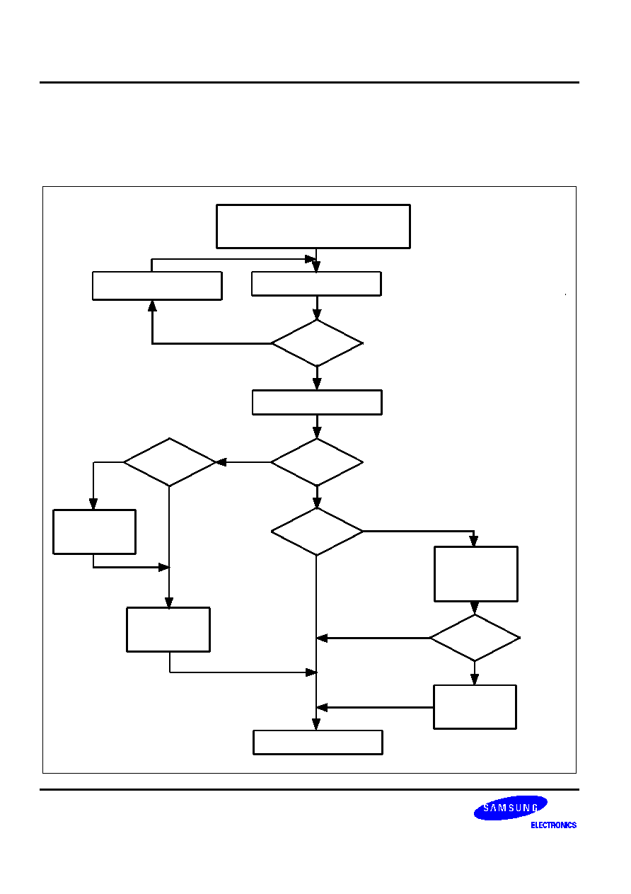
Write to configuration register
Set CDS or SHA operation
Set 3 or 1 channel mode
Set color pointer
Set clamp mode
Write to PGA gain register
Set to gain of one(00001)
Write to input offset register
Set to 0mV(10000000)
Set another color
YES
NO
P
P
O
O
W
W
E
E
R
R
-
-
O
O
N
N
I
I
N
N
I
I
T
T
I
I
A
A
L
L
I
I
Z
Z
A
A
T
T
I
I
O
O
N
N
C
C
A
A
L
L
I
I
B
B
R
R
A
A
T
T
I
I
O
O
N
N
Decide clamp level for SHA mode
(Refer to next page)
Set PGA gain
(Input offset = 0 mV)
Set another color
YES
NO
Scan dark line
Compute pixel offsets
Set input offset
Set odd/even offset in back end
Set gain/offset bus size
in back end
Set external pixel offset
in back end
Scan white line
Compute pixel gains
in back end
Adjust PGA gain
YES
NO
BW1222L
0.35
µ
µ
µ
µ
m AFE FOR CCD/CIS SIGNAL PROCESSOR
18
CIS
CLAMP
LEVEL
DECISION
FOR
EACH
INPUT
*Assume
that
PGA
gain
=
1.
The
user
can
modify
this
alogorithm
as
required
in
overall
system
ADC output > 0
YES
NO
Scan clamp level input
Decrease CIS clamp control
register by 1
Write CIS clamp control register
Set to (111)
Scan dark line
MIN(ADC output)
> 52
NO
MIN(ADC output)
> 104
NO
YES
MIN(ADC output)
> 0
YES
Go to calibration
Increase CIS
clamp control
register by 1
Increase CIS
clamp control
register by 1
YES
MIN(ADC output)
> 52
YES
NO
Decrease CIS
clamp control
register by 1.
Scan dark line
NO
Increase CIS
clamp control
register by 1
[MIN(ADC output) = Minimum value of all pixels]
[Repeatedly, scan clamp level.
Average ADC output]
[(100mV)/(2V) * 1024 -1 = 52]

0.35
µ
µ
µ
µ
m AFE FOR CCD/CIS SIGNAL PROCESSOR
BW1222L
19
CORE
EVALUATION
GUIDE
bw1222l
R_VIN
ADCCLK
MCTL1,MCTL2
D[9:0]
REFT
AD[2:0]
CSB
WRB
RDB
OEB
EXT_MCTL
TEST_S1,TESTS2
TEST_OUT
CDS2_CLK
CDS1_CLK
STRTLN
G_VIN
R_VIN
B_VIN
R_VIN
VCOM
REFB
0.1u
0.1u
0.1u
TIMING GENERATOR
MPU INTERFACE
DSP ASIC
MUX
MUX
Externally forced digital input/output
VDDA1,VDDA2
VSSA1,VSSA2,VBBA
VDDA3,VDDA4
VSSA3,VSSA4
TEST_CTL
2
2
10
3
3
2
2
2

BW1222L
0.35
µ
µ
µ
µ
m AFE FOR CCD/CIS SIGNAL PROCESSOR
20
PACKAGE
CONFIGURATION
The digital pins should be well decoupled to the analog ground plane.
ITEST
STBY
SPEEDUP
NC
NC
NC
NC
VBBA
VSSA1
VSSA1
VDDA1
VDDA1
IBIAS
B_VIN
G_VIN
R_VIN
D[7]
D[8]
D[9]
INDEX1
INDEX2
TEST_S1
TEST_S2
TEST_CTL
NC
NC
EXT_MCTL
MCTL1
MCTL2
AD[0]
AD[1]
AD[2]
R
E
F
B
R
E
F
T
V
C
O
M
N
C
V
S
S
A
3
V
S
S
A
3
V
D
D
A
3
V
D
D
A
3
S
T
R
T
L
N
C
D
S
1
_
C
L
K
C
D
S
2
_
C
L
K
A
D
C
C
L
K
O
E
B
W
R
B
R
D
B
C
S
B
T
E
S
T
_
O
U
T
V
D
D
A
2
V
D
D
A
4
D
[
0
]
D
[
1
]
D
[
2
]
D
[
3
]
D
[
4
]
D
[
5
]
D
[
6
]
V
D
D
A
2
V
S
S
A
2
V
S
S
A
2
V
S
S
A
4
V
S
S
A
4
V
D
D
A
4
0.01u
50
0.01u
50
0.01u
50
0.1u
0.1u
10u
0.1u
0.1u
10u
0.1u
10u
50
10u
0.1u
50
50
BW1222L
0.1u
10u

0.35
µ
µ
µ
µ
m AFE FOR CCD/CIS SIGNAL PROCESSOR
BW1222L
21
PACKAGE
PIN
DESCRIPTION
Pin No.
Pin Name
I/O Type
Description
1
TEST_OUT
AO
Analog Output in Test Mode
2
VDDA2
AP
Analog Power for A/D Converter
3
VDDA2
AP
Analog Power for A/D Converter
4
VSSA2
AG
Analog Ground for A/D Converter
5
VSSA2
AG
Analog Ground for A/D Converter
6
VSSA4
DG
Output Buffer Ground
7
VSSA4
DG
Output Buffer Ground
8
VDDA4
DP
Output Buffer Power
9
VDDA4
DP
Output Buffer Power
10
D[0]
DB
Digital Output (LSB)
11
D[1]
DB
Digital Output
12
D[2]
DB
Digital Output
13
D[3]
DB
Digital Output
14
D[4]
DB
Digital Output
15
D[5]
DB
Digital Output
16
D[6]
DB
Digital Output
17
D[7]
DB
Digital Output
18
D[8]
DB
Digital Output
19
D[9]
DB
Digital Output (MSB)
20
INDEX1
≠
Index Resistor(+)
21
INDEX2
≠
Index Resistor(-)
22
TEST_S1
DI
Color Pointer in Test Mode
23
TEST_S2
DI
Color Pointer in Test Mode
24
TEST_CTL
DI
Test Mode Control (Active Low)
25
NC
≠
Not Connected
26
NC
≠
Not Connected
27
EXT_MCTL
DI
MUX Control Mode Selection(Active Low)
28
MCTL1
DI
Color Pointer for MUX Control
29
MCTL2
DI
Color Pointer for MUX Control
30
AD[0]
DI
Register Selection Pin
31
AD[1]
DI
Register Selection Pin
32
AD[2]
DI
Register Selection Pin

BW1222L
0.35
µ
µ
µ
µ
m AFE FOR CCD/CIS SIGNAL PROCESSOR
22
PACKAGE
PIN
DESCRIPTION (Continued)
Pin No.
Pin Name
I/O Type
Description
33
CSB
DI
Chip Selection (Active Low)
34
RDB
DI
Read Strobe (Active Low)
35
WRB
DI
Write Strobe (Active Low)
36
OEB
DI
Output Enable (Active Low)
37
ADCCLK
DI
A/D Converter Clock Input
38
CDS2_CLK
DI
CDS Data Clock Input
39
CDS1_CLK
DI
CDS Reset Clock Input
40
STRTLN
DI
Start Line (Active Low)
41
VDDA3
DP
Digital Power
42
VDDA3
DP
Digital Power
43
VSSA3
DG
Digital Ground
44
VSSA3
DG
Digital Ground
45
NC
≠
Not Connected
46
VCOM
AB
Reference Middle Voltage
47
REFT
AB
Reference Top Voltage
48
REFB
AB
Reference Bottom Voltage
49
R_VIN
AI
Red Analog Input
50
G_VIN
AI
Green Analog Input
51
B_VIN
AI
Blue Analog Input
52
IBIAS
AB
Current Bias Control for CDS & PGA
53
VDDA1
AP
Analog Power
54
VDDA1
AP
Analog Power
55
VSSA1
AG
Analog Ground
56
VSSA1
AG
Analog Ground
57
VBBA
AG
Analog Ground
58
NC
≠
Not Connected
59
NC
≠
Not Connected
60
NC
≠
Not Connected
61
NC
≠
Not Connected
62
SPEEDUP
AI
Speed-Up Selection for A/D Converter
63
STBY
AI
Power Down Mode for A/D Converter
64
ITEST
AB
Current Bias Control for A/D Converter
0.35
µ
µ
µ
µ
m AFE FOR CCD/CIS SIGNAL PROCESSOR
BW1222L
23
USER
GUIDE
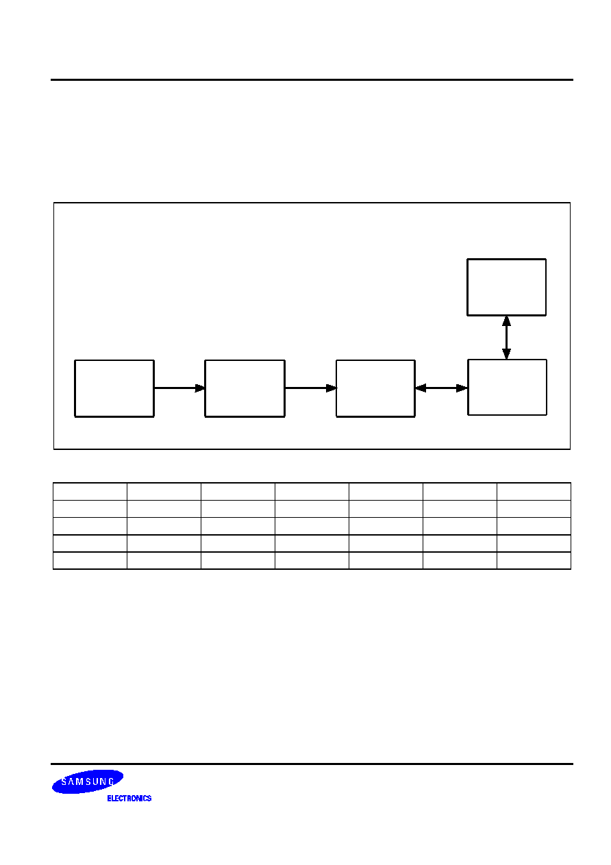
SYSTEM CONFIGURATION
It is necessary that output signal of analog front end be shading-compensated by back end logic block including
subtracter and multiplier.
(Shading-Compensation Block)
CCD/CIS
AFE
Subtracter
Multiplier
Controller
Memory
Table 2. Output Bus Controls
CSB
0
0
0
0
1
1
WRB
0
1
1
1
x
x
RDB
1
x
0
x
x
x
OEB
1
0
x
1
0
1
DOUT
MPU Input
X
MPU Output
Z
ADC Output
Z
NOTE: x: Don't Care X: Unknown (Not recommended)
Z: High Impedance

BW1222L
0.35
µ
µ
µ
µ
m AFE FOR CCD/CIS SIGNAL PROCESSOR
24
FEEDBACK REQUEST
SPECIFICATION
Characteristics
Symbol
Min
Typ
Max
Unit
Comment
Resolution
Bits
Signal-to-Noise &
Distortion Ratio
SNDR
dB
Conversion Rate
3-Channel with CDS
1-Channel with CDS
MSPS
MSPS
Differential
Nonlinearity
DNL
LSB
Integral
Nonlinearity
INL
LSB
Unipolar Offset Error
%FSR
Gain Error
%FSR
Anlog Input
Full-Scale Input
Vp-p
Power Supply
Analog Voltage
Digital Voltage
VDDA
VDDD
V
V
Power Consumption
mW
Temperature Range
∞
C
-- What do you want to choose as power supply voltages? For example, the analog VDD needs to be 3V.
The digital VDD can be 3.3V/5V.
-- Which modes of AFE do you use for overall system ? (Refer to page 9)
-- Would you define the gain range and input offset range ?
-- Could you explain external/internal pin configurations as required?
-- Should the bus interface be compatible with TTL ?
-- If possible, present other requirements below.
0.35
µ
µ
µ
µ
m AFE FOR CCD/CIS SIGNAL PROCESSOR
BW1222L
25
HISTORY CARD
Version
Date
Modified Items
Comments
ver 1.0
Original version published (preliminary)
ver 1.1
ver 1.2
ver 1.3
ver 1.4
1998.10
Release the formal datasheet

BW1222L
0.35
µ
µ
µ
µ
m AFE FOR CCD/CIS SIGNAL PROCESSOR
26
NOTES