0.35
µ
µ
µ
µ
m 10-BIT 500KSPS/8-BIT 650KSPS ADC
BW1227L
1
GENERAL DESCRIPTION
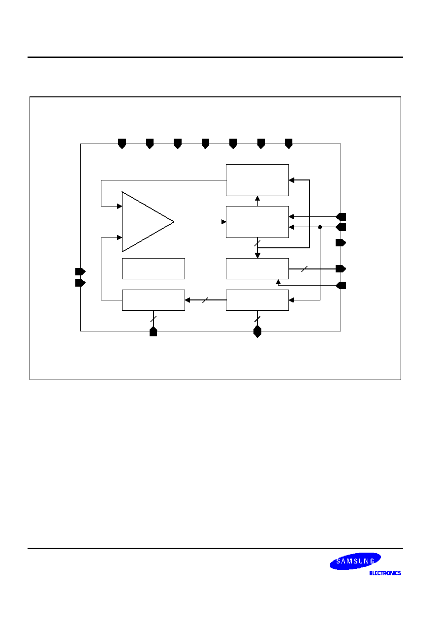
The BW1227L is a CMOS 8bit/10bit changeable A/D converter which combines an 8-channel analog input MUX,
auto offset calibration comparator, high resolution R-string DAC, clock generator, 8bit/10bit changeable successive
approximation register (SAR), output register, and AISC which controls analog input selection. BW1227L provides
a hardwired MODE8 pin and software-selection power-down mode. At the MODE8 state is "low", the device
operates as 10bit ADC, and if "high", operates as 8bit. The device operates with a single +3.3V supply and A/D
conversion rate is 500KSPS at 10bit and 650KSPS at 8bit, external clock XP1 is 25MHz. The operating
temperature range is 0~70 ∞C for commercial spec. Even if The BW1227L is fabricated with 48TSSOP package
but the USER can select a fit package using the CORE.
FEATURES
-- Resolution: 10 bit
-- Differential Linearity Error: ±1.0 LSB
-- Integral Linearity Error: ±2.0 LSB
-- Maximum Conversion Rate: 500KSPS (10bit)
650KSPS (8bit)
-- Low Power Consumption
: at operating, 3.3mW(typ)
: at standby, 330nW(typ)
-- Power Supply Voltage: 3.3V single(typ)
-- Guaranteed Monotonicity
-- No Missing Code
-- Latched Tri-state Output
-- Operation Temperature Range : 0 ~70
∞
C
0.35
µ
µ
µ
µ
m 10-BIT 500KSPS/8-BIT 650KSPS ADC
BW1227L
3
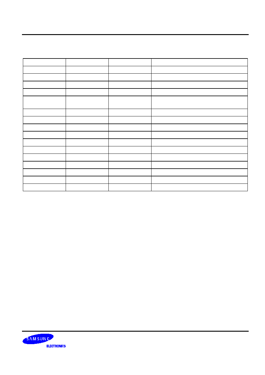
CORE PIN DESCRIPTION
Name
I/O Type
I/O Pad
Pin Description
REFP
AI
pia_bb
Internal Reference Top Bias. 3.3V
REFN
AI
pia_bb
Internal Reference Bottom Bias. 0V
VDDA
AP
vdda
Analog Power(3.3V)
VSSA
AG
vssa
Analog Ground
AIN[7:0]
AI
piar50_bb
Analog Inputs.
Input Span: REFP ~ REFN
MODE8
DI
picc_bb
10bit/8bit Mode Change Enable Pin
XP1
DI
picc_bb
Main Clock(external)
STBY
DI
picc_bb
System Power Down(Active High)
ADEN
DI
picc_bb
A/D Conversion Enable
ADO[9:0]
DO
pot2_bb
Digital Outputs
DGET
DI
picc_bb
DOUTs Read Enable
ASEL[2:0]
DB
poa_bb
AIN Selection Pins, Bidirectional.
FLAG
DO
pot2_bb
Test pin for checking the ADC state
VBBA
DG/AG
vbba
Sub Bias
VSSD
DG
vssd
Digital Ground
VDDD
DP
vddd
Digital Power
I/O Type Abbr.
-- AI: Analog Input
-- DI: Digital Input
-- AO: Analog Output
-- DO: Analog Output
-- AP: Analog Power
-- AG: Analog Ground
-- DP: Digital Power
-- DG: Digital Ground
-- AB: Analog Bidirection
-- DB: Digital Bidirection
0.35
µ
µ
µ
µ
m 10-BIT 500KSPS/8-BIT 650KSPS ADC
BW1227L
5
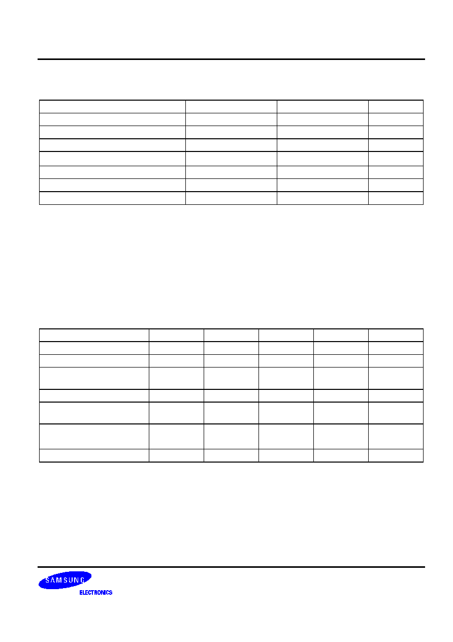
ABSOLUTE MAXIMUM RATINGS
Characteristics
Symbol
Value
Unit
Supply Voltage
VDD
4.5
V
Analog Input Voltage
AIN
VSS to VDD
V
Digital Input Voltage
DIN
VSS to VDD
V
Digital Output Voltage
V
OH
, V
OL
VSS to VDD
V
Reference Voltage
REFP / REFN
VSS to VDD
V
Storage Temperature Range
Tstg
-45 to 150
∞
C
Operating Temperature Range
Topr
0 to 70
∞
C
NOTES
1.
ABSOLUTE
MAXIMUM
RATING
specifies
the
values
beyond
which
the
device
may
be
damaged
permanently.
Exposure
to
ABSOLUTE
MAXIMUM
RATING
conditions
for
extended
periods
may
affect
reliability.
Each
condition
value
is
applied
with
the
other
values
kept
within
the
following
operating
conditions
and
function
operation
under
any
of
these
conditions
is
not
implied.
2.
All
voltages
are
measured
with
respect
to
VSS
unless
otherwise
specified.
3.
100pF
capacitor
is
discharged
through
a
1.5k
resistor
(Human
body
model)
RECOMMENDED OPERATING CONDITIONS
Characteristics
Symbol
Min
Typ
Max
Unit
Supply Voltage
VDDA,VDDD
3.3-5%
3.3
3.3+5%
V
Supply Voltage Difference
VDDA-VDDD
-0.1
0.0
0.1
V
Reference Input Voltage
REFP
REFN
≠
≠
VDDA
0
≠
≠
V
Analog Input Voltage
AIN
REFN
≠
REFP
V
Clock High Time
Clock Low Time
Tpwh
Tpwl
≠
≠
19
19
≠
≠
ns
Digital Input 'L' Voltage
Digital Input 'H' Voltage
V
IL
V
IH
0
0.9*VDDD
≠
≠
0.1*VDDD
VDDD
V
Operating Temperature
Topr
0
≠
70
∞
C
NOTE: It
is
strongly
recommended
that
all
the
supply
pins
(VDDA,
VDDD)
be
powered
from
the
same
source
to
avoid
power
latch-up.